Fig. 1.
(a) A conventional DL. (b) Timing diagram of the conventional DL.
SEMICONDUCTOR INTEGRATED CIRCUITS
Dandan Zhang1, 2, Wenrui Zhu1, 2, Wei Li1, Zhihong Huang1, 2, Lijiang Gao1 and Haigang Yang1,
Corresponding author: Yang Haigang, Email:yanghg@mail.ie.ac.cn
Abstract: A multimode DLL with trade-off between multiphase and static phase error is presented. By adopting a multimode control circuit to regroup the delay line, a better static phase error performance can be achieved while reducing the number of output phases. The DLL accomplishes three operation modes:mode1 with a four-phase output, mode2 with a two-phase output and a better static phase error performance, and mode3 with only a one-phase output but the best static phase error performance. The proposed DLL has been fabricated in 0.13 μm CMOS technology and measurement results show that the static phase errors of mode1, mode2 and mode3 are -18.2 ps, 11.8 ps and -6.44 ps, respectively, at 200 MHz. The measured RMS and peak-to-peak jitters of mode1, mode2 and mode3 are 2.0 ps, 2.2 ps, 2.1 ps and 10 ps, 9.3 ps, 10 ps respectively.
Keywords: DLL, multimode, multiphase, static phase error
| [1] |
Chien G, Gray P R. A 900 MHz local oscillator using a DLL-based frequency multiplier technique for PCS application. IEEE J Solid-State Circuits, 2000, 35(12):1995 http://www.academia.edu/1063532/A_900-MHz_local_oscillator_using_a_DLL-based_frequency_multiplier_technique_for_PCS_applications
|
| [2] |
Chang H H, Chang J Y, Kuo C Y, et al. A 0.7-2-GHz self-calibrated multiphase delay-locked loop. IEEE J Solid-State Circuits, 2006, 41(5):1051 doi: 10.1109/JSSC.2006.874036
|
| [3] |
Chang H H, Yang R J, Liu S I. Low jitter and multirate clock and data recovery circuit using a MSADLL for chip-to-chip interconnection. IEEE Trans Circuit Syst I, Reg Papers, 2004, 51(12):2356 doi: 10.1109/TCSI.2004.838147
|
| [4] |
Kim Y S, Lee S K, Park H J, et al. A 110 MHz to 1.4 GHz locking 40-phase all-digital DLL. IEEE J Solid-State Circuits, 2011, 46(2):435 doi: 10.1109/JSSC.2010.2092996
|
| [5] |
Lin S C, Lee T C. An 833-MHz 132-phase multiphase clock generator with self-calibration circuits. IEEE Asian Solid-State Circuits Conference, 2008:437 http://iopscience.iop.org/export?articleId=1674-4926/35/5/055010&exportFormat=iopexport_bib&exportType=refs&navsubmit=Export%2Breferences
|
| [6] |
Bae J H, Seo J H, Yeo H S, et al. An all-digital 90-degree phase-shift dll with loop-embedded DCC for 1.6 Gbps DDR interface. IEEE Custom Integrated Circuits Conference (CICC), 2007:373 doi: 10.1007/s11432-014-5226-1
|
| [7] |
Chen Zhujia, Yang Haigang, Liu Fei, et al. A fast-locking all-digital delay-locked loop for phase/delay generation in an FPGA. Journal of Semiconductors, 2011, 32(10):105010 doi: 10.1088/1674-4926/32/10/105010
|
| [8] |
Zhang D, Yang H, Chen Z, et al. A fast-locking digital DLL with a high resolution time-to-digital converter. IEEE Custom Integrated Circuits Conference (CICC), 2013:1 http://www.ijsr.net/archive/v4i7/SUB156578.pdf
|
| [9] |
Lin W M, Teng K F, Liu S I. A delay-locked loop with digital background calibration. IEEE Asian Solid-State Circuits Conference, 2009:317 http://www.eecg.utoronto.ca/~tcc/samarah_cicc2012.pdf
|
| [10] |
Ryu K, Jung D H, Jung S O. A DLL with dual edge triggered phase detector for fast lock and low jitter clock generator. IEEE Trans Circuits Syst I:Regular Papers (TSCAS-I), 2012, 59(9):1860 doi: 10.1109/TCSI.2011.2180453
|
| [11] |
Park J H, Jung D H, Ryu K, et al. ADDLL for clock-Deskew buffer in high-performance SoCs. IEEE Trans Very Large Scale Integration (VLSI) Syst, 2013, 21(7):1368 doi: 10.1109/TVLSI.2012.2210742
|
| [12] |
Jung D H, Ryu K, Park J H, et al. A low-power and small-area all-digital delay-locked loop with closed-loop duty-cycle correction. Proceedings of the ESSCIRC (ESSCIRC), 2012:181 doi: 10.1007/s11432-014-5226-1
|
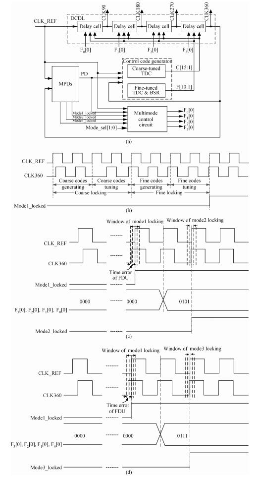
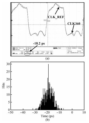
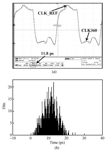
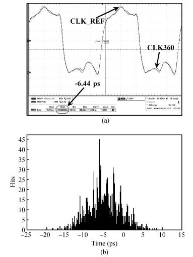
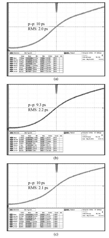
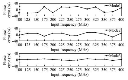
Table 1. Performance comparison
 |
| [1] |
Chien G, Gray P R. A 900 MHz local oscillator using a DLL-based frequency multiplier technique for PCS application. IEEE J Solid-State Circuits, 2000, 35(12):1995 http://www.academia.edu/1063532/A_900-MHz_local_oscillator_using_a_DLL-based_frequency_multiplier_technique_for_PCS_applications
|
| [2] |
Chang H H, Chang J Y, Kuo C Y, et al. A 0.7-2-GHz self-calibrated multiphase delay-locked loop. IEEE J Solid-State Circuits, 2006, 41(5):1051 doi: 10.1109/JSSC.2006.874036
|
| [3] |
Chang H H, Yang R J, Liu S I. Low jitter and multirate clock and data recovery circuit using a MSADLL for chip-to-chip interconnection. IEEE Trans Circuit Syst I, Reg Papers, 2004, 51(12):2356 doi: 10.1109/TCSI.2004.838147
|
| [4] |
Kim Y S, Lee S K, Park H J, et al. A 110 MHz to 1.4 GHz locking 40-phase all-digital DLL. IEEE J Solid-State Circuits, 2011, 46(2):435 doi: 10.1109/JSSC.2010.2092996
|
| [5] |
Lin S C, Lee T C. An 833-MHz 132-phase multiphase clock generator with self-calibration circuits. IEEE Asian Solid-State Circuits Conference, 2008:437 http://iopscience.iop.org/export?articleId=1674-4926/35/5/055010&exportFormat=iopexport_bib&exportType=refs&navsubmit=Export%2Breferences
|
| [6] |
Bae J H, Seo J H, Yeo H S, et al. An all-digital 90-degree phase-shift dll with loop-embedded DCC for 1.6 Gbps DDR interface. IEEE Custom Integrated Circuits Conference (CICC), 2007:373 doi: 10.1007/s11432-014-5226-1
|
| [7] |
Chen Zhujia, Yang Haigang, Liu Fei, et al. A fast-locking all-digital delay-locked loop for phase/delay generation in an FPGA. Journal of Semiconductors, 2011, 32(10):105010 doi: 10.1088/1674-4926/32/10/105010
|
| [8] |
Zhang D, Yang H, Chen Z, et al. A fast-locking digital DLL with a high resolution time-to-digital converter. IEEE Custom Integrated Circuits Conference (CICC), 2013:1 http://www.ijsr.net/archive/v4i7/SUB156578.pdf
|
| [9] |
Lin W M, Teng K F, Liu S I. A delay-locked loop with digital background calibration. IEEE Asian Solid-State Circuits Conference, 2009:317 http://www.eecg.utoronto.ca/~tcc/samarah_cicc2012.pdf
|
| [10] |
Ryu K, Jung D H, Jung S O. A DLL with dual edge triggered phase detector for fast lock and low jitter clock generator. IEEE Trans Circuits Syst I:Regular Papers (TSCAS-I), 2012, 59(9):1860 doi: 10.1109/TCSI.2011.2180453
|
| [11] |
Park J H, Jung D H, Ryu K, et al. ADDLL for clock-Deskew buffer in high-performance SoCs. IEEE Trans Very Large Scale Integration (VLSI) Syst, 2013, 21(7):1368 doi: 10.1109/TVLSI.2012.2210742
|
| [12] |
Jung D H, Ryu K, Park J H, et al. A low-power and small-area all-digital delay-locked loop with closed-loop duty-cycle correction. Proceedings of the ESSCIRC (ESSCIRC), 2012:181 doi: 10.1007/s11432-014-5226-1
|


Article views: 2984 Times PDF downloads: 21 Times Cited by: 0 Times
Received: 23 November 2013 Revised: 12 December 2013 Online: Published: 01 May 2014
| Citation: |
Dandan Zhang, Wenrui Zhu, Wei Li, Zhihong Huang, Lijiang Gao, Haigang Yang. A multimode DLL with trade-off between multiphase and static phase error[J]. Journal of Semiconductors, 2014, 35(5): 055010. doi: 10.1088/1674-4926/35/5/055010
****
Dandan Zhang and A Zhang, W R Zhu, W Li, Z H Huang, L J Gao, H G Yang. A multimode DLL with trade-off between multiphase and static phase error[J]. J. Semicond., 2014, 35(5): 055010. doi: 10.1088/1674-4926/35/5/055010.

|
| [1] |
Chien G, Gray P R. A 900 MHz local oscillator using a DLL-based frequency multiplier technique for PCS application. IEEE J Solid-State Circuits, 2000, 35(12):1995 http://www.academia.edu/1063532/A_900-MHz_local_oscillator_using_a_DLL-based_frequency_multiplier_technique_for_PCS_applications
|
| [2] |
Chang H H, Chang J Y, Kuo C Y, et al. A 0.7-2-GHz self-calibrated multiphase delay-locked loop. IEEE J Solid-State Circuits, 2006, 41(5):1051 doi: 10.1109/JSSC.2006.874036
|
| [3] |
Chang H H, Yang R J, Liu S I. Low jitter and multirate clock and data recovery circuit using a MSADLL for chip-to-chip interconnection. IEEE Trans Circuit Syst I, Reg Papers, 2004, 51(12):2356 doi: 10.1109/TCSI.2004.838147
|
| [4] |
Kim Y S, Lee S K, Park H J, et al. A 110 MHz to 1.4 GHz locking 40-phase all-digital DLL. IEEE J Solid-State Circuits, 2011, 46(2):435 doi: 10.1109/JSSC.2010.2092996
|
| [5] |
Lin S C, Lee T C. An 833-MHz 132-phase multiphase clock generator with self-calibration circuits. IEEE Asian Solid-State Circuits Conference, 2008:437 http://iopscience.iop.org/export?articleId=1674-4926/35/5/055010&exportFormat=iopexport_bib&exportType=refs&navsubmit=Export%2Breferences
|
| [6] |
Bae J H, Seo J H, Yeo H S, et al. An all-digital 90-degree phase-shift dll with loop-embedded DCC for 1.6 Gbps DDR interface. IEEE Custom Integrated Circuits Conference (CICC), 2007:373 doi: 10.1007/s11432-014-5226-1
|
| [7] |
Chen Zhujia, Yang Haigang, Liu Fei, et al. A fast-locking all-digital delay-locked loop for phase/delay generation in an FPGA. Journal of Semiconductors, 2011, 32(10):105010 doi: 10.1088/1674-4926/32/10/105010
|
| [8] |
Zhang D, Yang H, Chen Z, et al. A fast-locking digital DLL with a high resolution time-to-digital converter. IEEE Custom Integrated Circuits Conference (CICC), 2013:1 http://www.ijsr.net/archive/v4i7/SUB156578.pdf
|
| [9] |
Lin W M, Teng K F, Liu S I. A delay-locked loop with digital background calibration. IEEE Asian Solid-State Circuits Conference, 2009:317 http://www.eecg.utoronto.ca/~tcc/samarah_cicc2012.pdf
|
| [10] |
Ryu K, Jung D H, Jung S O. A DLL with dual edge triggered phase detector for fast lock and low jitter clock generator. IEEE Trans Circuits Syst I:Regular Papers (TSCAS-I), 2012, 59(9):1860 doi: 10.1109/TCSI.2011.2180453
|
| [11] |
Park J H, Jung D H, Ryu K, et al. ADDLL for clock-Deskew buffer in high-performance SoCs. IEEE Trans Very Large Scale Integration (VLSI) Syst, 2013, 21(7):1368 doi: 10.1109/TVLSI.2012.2210742
|
| [12] |
Jung D H, Ryu K, Park J H, et al. A low-power and small-area all-digital delay-locked loop with closed-loop duty-cycle correction. Proceedings of the ESSCIRC (ESSCIRC), 2012:181 doi: 10.1007/s11432-014-5226-1
|

 WeChat ID
Journal of Semiconductors © 2017 All Rights Reserved 京ICP备05085259号-2

 DownLoad: