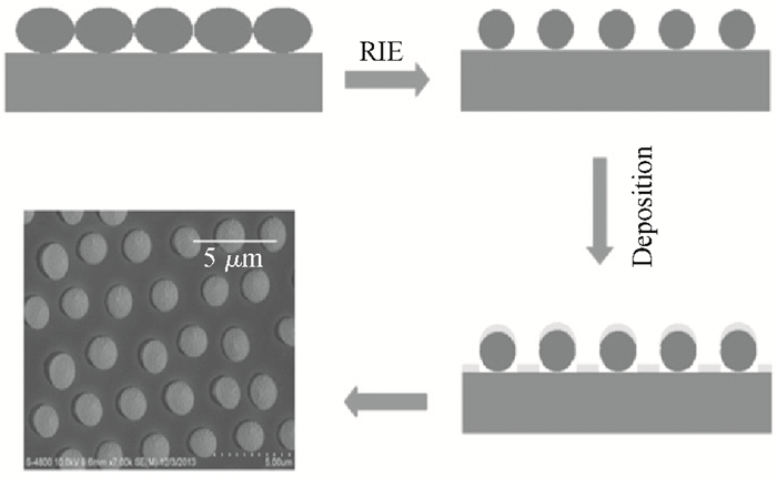
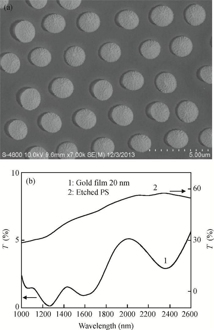
Fig. 1.
Schematic representation of the sample fabrication and the SEM picture of the sample.
SEMICONDUCTOR PHYSICS
Jing Ju, Yuqin Zhou and Gangqiang Dong
Corresponding author: Zhou Yuqin, Email:yqzhou@ucas.ac.cn
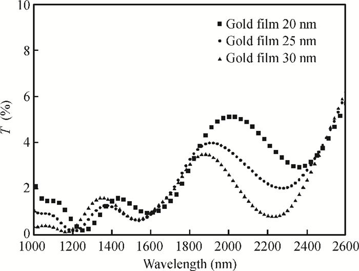
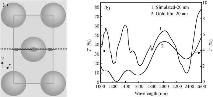
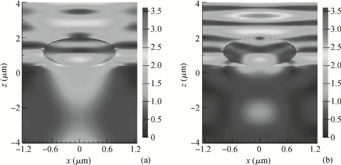
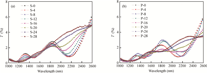
Abstract: We studied the infrared transmission properties of gold films on ordered two-dimensional non-close-packed polystyrene (PS) colloidal crystal. The gold films consist of gold half-shells on the PS spheres and gold film with 2D arrays of holes on the glass substrate. An extraordinary optical transmission phenomenon could be found in such a structure. Simulations with the finite-difference time-domain method were also employed to get the transmission spectra and electric field distribution. The transmission response of the samples can be adjusted by controlling the thickness of the gold films. Angle-resolved measurements were performed using polarized light to obtain more information about the surface plasmon polariton resonances of the gold films. As the angle changes, the transmission spectra change a lot. The transmission spectra of p-polarized light have quite different properties compared to those of s-polarized light.
Keywords: SPP, extraordinary optical transmission, non-close-packed colloidal crystal, polarized light
| [1] |
Ebbesen T W, Lezec H J, Ghaemi H F, et al. Extraordinary optical transmission through sub-wavelength hole arrays. Nature, 1998, 391:667 doi: 10.1038/35570
|
| [2] |
Martín-Moreno L, García-Vidal F J, Lezec H J, et al. Theory of extraordinary optical transmission through subwavelength hole arrays. Phys Rev Lett, 2001, 86:1114 doi: 10.1103/PhysRevLett.86.1114
|
| [3] |
Bravo-Abad J, Degiron A, Przybilla F, et al. How light emerges from an illuminated array of subwavelength holes. Nature Phys, 2006, 2:120 doi: 10.1038/nphys213
|
| [4] |
Miyamaru F, Kamijyo M, Takano K, et al. Characteristics and generation process of surface waves excited on a perfect conductor surface. Opt Express, 2010, 18(16):17576 doi: 10.1364/OE.18.017576
|
| [5] |
Degiron A, Lezec H J, Barnes W L, et al. Effects of hole depth on enhanced light transmission through subwavelength hole arrays. Appl Phys Lett, 2002, 81:4327 doi: 10.1063/1.1526162
|
| [6] |
Kim T J, Thio T, Ebbesen T W, et al. Control of optical transmission through metals perforated with subwavelength hole arrays. Opt Lett, 1999, 24:256 doi: 10.1364/OL.24.000256
|
| [7] |
Zhan P, Wang Z L, Dong H, et al. The anomalous infrared transmission of gold films on two-dimensional colloidal crystals. Adv Mater, 2006, 18:1612 doi: 10.1002/(ISSN)1521-4095
|
| [8] |
Wang Z B, Ye Y H, Zhang Y A, et al. Visible transmission through metal-coated colloidal crystals. Appl Phys A, 2009, 97:225 doi: 10.1007/s00339-009-5184-4
|
| [9] |
Cai Z Y, Liu Y J, Leong E S P. Highly ordered and gap controllable two-dimensional non-close-packed colloidal crystals and plasmonic-photonic crystals with enhanced optical transmission. J Mater Chem, 2012, 22:24668 doi: 10.1039/c2jm34896a
|
| [10] |
Farcau C, Giloan M, Vinteler E, et al. Understanding plasmon resonances of metal-coated colloidal crystal monolayers. Appl Phys B, 2012, 106:849 doi: 10.1007/s00340-011-4849-9
|
| [11] |
Endo T, Takizawa H, Imai Y, et al. Study of electrical field distribution of gold-capped nanoparticle for excitation of localized surface plasmon resonance. Appl Surf Sci, 2011, 257:2560 doi: 10.1016/j.apsusc.2010.10.022
|
| [12] |
Haynes C L, Van Duyne R P. Nanosphere lithography:a versatile nanofabrication tool for studies of size-dependent nanoparticle optics. J Phys Chem B, 2001, 105:5599 doi: 10.1021/jp010657m
|
| [13] |
Walsh G F, Negro L D. Engineering plasmon-enhanced Au light emission with planar arrays of nanoparticles. Nano Lett, 2013, 13:786 doi: 10.1021/nl304523v
|
| [14] |
Bhattacharya J, Chakravarty N, Pattnaik S, et al. Comparison of optical properties of periodic photonic-plasmonic and randomly textured back reflectors for nc-Si solar cells. Journal of Non-Crystalline Solids, 2012, 358:2313 doi: 10.1016/j.jnoncrysol.2011.12.108
|
| [15] |
Ferry V E, Verschuuren M A, Li H B T, et al. Light trapping in ultrathin plasmonic solar cells. Opt Express, 2010, 18(S2):A237 doi: 10.1364/OE.18.00A237
|
| [16] |
Pan F, Zhang J Y, Cai C, et al. Rapid fabrication of large-area colloidal crystal monolayers by a vertical surface method. Langmuir, 2006, 22(17):7101 doi: 10.1021/la053323n
|
| [17] |
Ghaemi H F, Thio T, Grupp D E. Surface plasmons enhance optical transmission through subwavelength holes. Phys Rev B, 1998, 58(11):6779 doi: 10.1103/PhysRevB.58.6779
|
| [18] |
Jensen T R, Malinsky M D, Haynes C L, et al. Nanosphere lithography:tunable localized surface plasmon resonance spectra of silver nanoparticles. J Phys Chem B, 2000, 104:10549 doi: 10.1021/jp002435e
|
| [19] |
Rather H. Surface plasmons on smooth and rough surfaces and on gratings. Berlin:Springer, 1988
|


Article views: 3284 Times PDF downloads: 56 Times Cited by: 0 Times
Received: 21 February 2014 Revised: 08 April 2014 Online: Published: 01 September 2014
| Citation: |
Jing Ju, Yuqin Zhou, Gangqiang Dong. The infrared transmission through gold films on ordered two-dimensional non-close-packed colloidal crystals[J]. Journal of Semiconductors, 2014, 35(9): 092001. doi: 10.1088/1674-4926/35/9/092001
****
J Ju, Y Q Zhou, G Q Dong. The infrared transmission through gold films on ordered two-dimensional non-close-packed colloidal crystals[J]. J. Semicond., 2014, 35(9): 092001. doi: 10.1088/1674-4926/35/9/092001.

|
| [1] |
Ebbesen T W, Lezec H J, Ghaemi H F, et al. Extraordinary optical transmission through sub-wavelength hole arrays. Nature, 1998, 391:667 doi: 10.1038/35570
|
| [2] |
Martín-Moreno L, García-Vidal F J, Lezec H J, et al. Theory of extraordinary optical transmission through subwavelength hole arrays. Phys Rev Lett, 2001, 86:1114 doi: 10.1103/PhysRevLett.86.1114
|
| [3] |
Bravo-Abad J, Degiron A, Przybilla F, et al. How light emerges from an illuminated array of subwavelength holes. Nature Phys, 2006, 2:120 doi: 10.1038/nphys213
|
| [4] |
Miyamaru F, Kamijyo M, Takano K, et al. Characteristics and generation process of surface waves excited on a perfect conductor surface. Opt Express, 2010, 18(16):17576 doi: 10.1364/OE.18.017576
|
| [5] |
Degiron A, Lezec H J, Barnes W L, et al. Effects of hole depth on enhanced light transmission through subwavelength hole arrays. Appl Phys Lett, 2002, 81:4327 doi: 10.1063/1.1526162
|
| [6] |
Kim T J, Thio T, Ebbesen T W, et al. Control of optical transmission through metals perforated with subwavelength hole arrays. Opt Lett, 1999, 24:256 doi: 10.1364/OL.24.000256
|
| [7] |
Zhan P, Wang Z L, Dong H, et al. The anomalous infrared transmission of gold films on two-dimensional colloidal crystals. Adv Mater, 2006, 18:1612 doi: 10.1002/(ISSN)1521-4095
|
| [8] |
Wang Z B, Ye Y H, Zhang Y A, et al. Visible transmission through metal-coated colloidal crystals. Appl Phys A, 2009, 97:225 doi: 10.1007/s00339-009-5184-4
|
| [9] |
Cai Z Y, Liu Y J, Leong E S P. Highly ordered and gap controllable two-dimensional non-close-packed colloidal crystals and plasmonic-photonic crystals with enhanced optical transmission. J Mater Chem, 2012, 22:24668 doi: 10.1039/c2jm34896a
|
| [10] |
Farcau C, Giloan M, Vinteler E, et al. Understanding plasmon resonances of metal-coated colloidal crystal monolayers. Appl Phys B, 2012, 106:849 doi: 10.1007/s00340-011-4849-9
|
| [11] |
Endo T, Takizawa H, Imai Y, et al. Study of electrical field distribution of gold-capped nanoparticle for excitation of localized surface plasmon resonance. Appl Surf Sci, 2011, 257:2560 doi: 10.1016/j.apsusc.2010.10.022
|
| [12] |
Haynes C L, Van Duyne R P. Nanosphere lithography:a versatile nanofabrication tool for studies of size-dependent nanoparticle optics. J Phys Chem B, 2001, 105:5599 doi: 10.1021/jp010657m
|
| [13] |
Walsh G F, Negro L D. Engineering plasmon-enhanced Au light emission with planar arrays of nanoparticles. Nano Lett, 2013, 13:786 doi: 10.1021/nl304523v
|
| [14] |
Bhattacharya J, Chakravarty N, Pattnaik S, et al. Comparison of optical properties of periodic photonic-plasmonic and randomly textured back reflectors for nc-Si solar cells. Journal of Non-Crystalline Solids, 2012, 358:2313 doi: 10.1016/j.jnoncrysol.2011.12.108
|
| [15] |
Ferry V E, Verschuuren M A, Li H B T, et al. Light trapping in ultrathin plasmonic solar cells. Opt Express, 2010, 18(S2):A237 doi: 10.1364/OE.18.00A237
|
| [16] |
Pan F, Zhang J Y, Cai C, et al. Rapid fabrication of large-area colloidal crystal monolayers by a vertical surface method. Langmuir, 2006, 22(17):7101 doi: 10.1021/la053323n
|
| [17] |
Ghaemi H F, Thio T, Grupp D E. Surface plasmons enhance optical transmission through subwavelength holes. Phys Rev B, 1998, 58(11):6779 doi: 10.1103/PhysRevB.58.6779
|
| [18] |
Jensen T R, Malinsky M D, Haynes C L, et al. Nanosphere lithography:tunable localized surface plasmon resonance spectra of silver nanoparticles. J Phys Chem B, 2000, 104:10549 doi: 10.1021/jp002435e
|
| [19] |
Rather H. Surface plasmons on smooth and rough surfaces and on gratings. Berlin:Springer, 1988
|

 WeChat ID
Journal of Semiconductors © 2017 All Rights Reserved 京ICP备05085259号-2

 DownLoad: