Fig. 1.
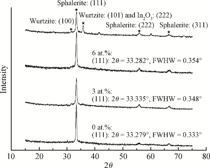
XRD patterns of 0, 3, 6, 9 at.% In-doped ZnS film
SEMICONDUCTOR MATERIALS
Corresponding author: Chen Jinhuo, Email:yeschen@fzu.edu.cn
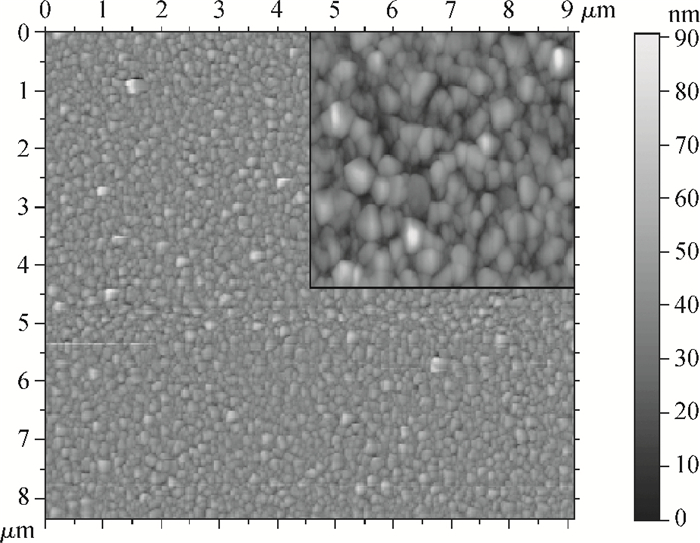
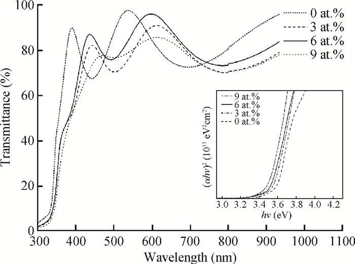
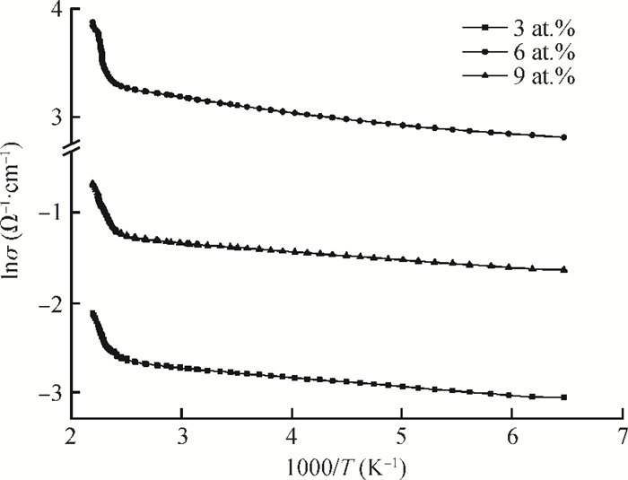
Abstract: This paper reports a new material, indium-doped ZnS (ZnS:In) film, which is fabricated for the first time to improve its electrical and optical performance. By electron beam evaporation technology and the optimized annealing treatment, high quality ZnS:In film is prepared. XRD indicates that the incorporation of 6 at.% indium atoms into ZnS film causes little lattice deformation. The AFM results imply that large sized particles are compactly dispersed in the ZnS:In layer and results in an unsmooth surface. Electrical and optical property tests show that the resistivity of ZnS film is greatly decreased to 4.46×10⁻² Ω·cm and the optical transmittance is improved to 85% in the visible region. Comparing with the results in other literatures, significant progress in electrical/optical performance has been made in this paper.
Keywords: ZnS, indium incorporation, thin film, semiconductors
| [1] |
Kasap S, Capper P. Springer handbook of electronic and photonic materials. Berlin:Springer, 2006
|
| [2] |
Hariskos D, Spiering S, Powalla M, et al. Buffer layers in Cu(In, Ga)Se2 solar cells and modules. Thin Solid Films, 2005, 480/481:99 http://ci.nii.ac.jp/naid/30006200708
|
| [3] |
Kreger F. The chemistry of imperfect crystals. Amsterdam:North-Holland, 1964
|
| [4] |
Contreras M A, Nakada T, Hongo M. ZnO/ZnS(O, OH)/Cu(In, Ga)Se2/Mo solar cell with 18.6% efficiency. Proceedings of 3rd World Conference on of Photovoltaic Energy Conversion, Osaka, Japan, 2003, 1:570 http://www.sciencedirect.com/science/article/pii/S0927024814000191
|
| [5] |
Nagamani, Revathi N, Prathapc P. Al-doped ZnS layers synthesized by solution growth method. Curr Aool Phys, 2012, 12:380 doi: 10.1016/j.cap.2011.07.031
|
| [6] |
Lott K, Nirk T, Shinkarenko S. High temperature electrical conductivity in ZnS:Al and in CdSe:Al. Solid State Ionics, 2004, 173:83 doi: 10.1016/j.ssi.2004.07.056
|
| [7] |
Prathap P, Revath N, Subbaiah Y P V. Preparation and characterization of transparent conducting ZnS:Al films. Solid State Sci, 2009, 11:224 doi: 10.1016/j.solidstatesciences.2008.04.020
|
| [8] |
Brus V V, Kovalyuk Z D, Maryanchuk P D. Optical properties of TiO-MnO thin films prepared by electron-beam evaporation. Tech Phys, 2012, 57:1148 doi: 10.1134/S1063784212080063
|
| [9] |
Cullity B D, Stock S R. Elements of X-ray diffraction. 3rd ed. New Jersey:Prentice Hall, 2001
|
| [10] |
Zhang R, Wang B, Wei L. Sulfidation growth and characterization of nanocrystalline ZnS thin films. Vacuum, 2008, 82:1208 doi: 10.1016/j.vacuum.2008.02.003
|


Article views: 3506 Times PDF downloads: 13 Times Cited by: 0 Times
Received: 02 March 2014 Revised: 20 April 2014 Online: Published: 01 September 2014
| Citation: |
Jinhuo Chen, Wenjian Li. Significant improvement of ZnS film electrical and optical performance by indium incorporation[J]. Journal of Semiconductors, 2014, 35(9): 093003. doi: 10.1088/1674-4926/35/9/093003
****
J H Chen, W J Li. Significant improvement of ZnS film electrical and optical performance by indium incorporation[J]. J. Semicond., 2014, 35(9): 093003. doi: 10.1088/1674-4926/35/9/093003.

|
| [1] |
Kasap S, Capper P. Springer handbook of electronic and photonic materials. Berlin:Springer, 2006
|
| [2] |
Hariskos D, Spiering S, Powalla M, et al. Buffer layers in Cu(In, Ga)Se2 solar cells and modules. Thin Solid Films, 2005, 480/481:99 http://ci.nii.ac.jp/naid/30006200708
|
| [3] |
Kreger F. The chemistry of imperfect crystals. Amsterdam:North-Holland, 1964
|
| [4] |
Contreras M A, Nakada T, Hongo M. ZnO/ZnS(O, OH)/Cu(In, Ga)Se2/Mo solar cell with 18.6% efficiency. Proceedings of 3rd World Conference on of Photovoltaic Energy Conversion, Osaka, Japan, 2003, 1:570 http://www.sciencedirect.com/science/article/pii/S0927024814000191
|
| [5] |
Nagamani, Revathi N, Prathapc P. Al-doped ZnS layers synthesized by solution growth method. Curr Aool Phys, 2012, 12:380 doi: 10.1016/j.cap.2011.07.031
|
| [6] |
Lott K, Nirk T, Shinkarenko S. High temperature electrical conductivity in ZnS:Al and in CdSe:Al. Solid State Ionics, 2004, 173:83 doi: 10.1016/j.ssi.2004.07.056
|
| [7] |
Prathap P, Revath N, Subbaiah Y P V. Preparation and characterization of transparent conducting ZnS:Al films. Solid State Sci, 2009, 11:224 doi: 10.1016/j.solidstatesciences.2008.04.020
|
| [8] |
Brus V V, Kovalyuk Z D, Maryanchuk P D. Optical properties of TiO-MnO thin films prepared by electron-beam evaporation. Tech Phys, 2012, 57:1148 doi: 10.1134/S1063784212080063
|
| [9] |
Cullity B D, Stock S R. Elements of X-ray diffraction. 3rd ed. New Jersey:Prentice Hall, 2001
|
| [10] |
Zhang R, Wang B, Wei L. Sulfidation growth and characterization of nanocrystalline ZnS thin films. Vacuum, 2008, 82:1208 doi: 10.1016/j.vacuum.2008.02.003
|

 WeChat ID
Journal of Semiconductors © 2017 All Rights Reserved 京ICP备05085259号-2

 DownLoad: