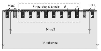
Fig. 1.
Schematic cross-section of the octagon-ring-shaped photodiode
SEMICONDUCTOR DEVICES
Changping Chen1, 2, Manfang Tian1, 2, Zhenyu Jiang1, 2, Xiangliang Jin1, 2, and Jun Luo3
Corresponding author: Jin Xiangliang, Email:jinxl@xtu.edu.cn
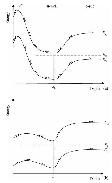
Abstract: A CMOS UV and blue-extended photodiode is presented and fabricated for light detection in the ultraviolet/blue spectral range. An octagon homocentric ring-shaped geometry is used to improve the ultraviolet responsivity and suppress edge breakdown. This paper has established a two-dimensional responsivity physical model for the presented photodiode and given some numerical analyses. The dead layer effect, which is caused by the high-doping effects and boron redistribution, is considered when analyzing the distribution of the current of the proposed UV and blue-extended photodiode. In the dead layer, the boron doping profile decreases towards the surface. Simulated results illustrate that the responsivity in the UV range is obviously decreased by the effect of the dead layer, while it is not affected in the visible and near-infrared part of the spectrum. The presented photodiode is fabricated and the silicon tested results are given, which agree well with the simulated ones.
Keywords: UV/blue-extended photodiode, responsivity physical model, dead layer effect, CMOS process
| [1] |
Charbon E. Towards large scale CMOS single-photon detector arrays for lab-on-chip applications. J Phys D:Appl Phys, 2008, 41(9):1
|
| [2] |
Chang Y W, Yu P C, Huang Y T, et al. A CMOS-compatible optical biosensing system based on visible absorption spectroscopy. Proceedings of IEEE Int Conf Electron Devices and Solid-State Circuits, Tainan, 2007
|
| [3] |
Pepin C M, Dautet H, Bergeron M, et al. New UV-enhanced, ultra-low noise silicon avalanche photodiode for radiation detection and medical imaging. Proceedings of Nuclear Science Symposium Conference Record (NSS/MIC), Knoxville, TN, 2010
|
| [4] |
Pauchard A, Besse P A, Popovic R S. A silicon blue/UV selective stripe-shaped photodiode. Sens Actuators, 1999, 76(1-3):172 doi: 10.1016/S0924-4247(99)00006-0
|
| [5] |
Ghazi A, Zimmermann H A, Seegebrecht P. CMOS photodiode with enhanced responsivity for the UV/blue spectral range. IEEE Trans Electron Devices, 2002, 49(7):1124 doi: 10.1109/TED.2002.1013266
|
| [6] |
Pauchard A, Rochas A, Randjelovic Z, et al. Ultraviolet avalanche photodiode in CMOS technology. Proceedings in IEDM Tech Dig, San Francisco CA, USA, 2000
|
| [7] |
Chang Y W, Huang Y T. The ring-shaped CMOS-based phototransistor with high responsivity for the UV/blue spectral range. IEEE Photonics Technol Lett, 2009, 21(13):899 doi: 10.1109/LPT.2009.2020176
|
| [8] |
Li Guike, Feng Peng, Wu Nanjian. A novel monolithic ultraviolet image sensor based on a standard CMOS process. Journal of Semiconductors, 2011, 32(10):105008 doi: 10.1088/1674-4926/32/10/105008
|
| [9] |
Esmaeili-Rad M R, Papadopoulos N P, Bauza M, et al. Blue-light-sensitive phototransistor for indirect X-ray image sensors. IEEE Electron Device Lett, 2012, 33(4):567 doi: 10.1109/LED.2012.2185676
|
| [10] |
Anderson B L, Anderson R L. Fundamentals of semiconductor devices (photocopy edition). 1st ed. Beijing:Tsinghua University Press, 2006
|
| [11] |
Jellison G E Jr. Optical functions of silicon determined by two-channel polarization modulation ellipsometry. Opt Mater, 1992, 1(1):41 doi: 10.1016/0925-3467(92)90015-F
|
| [12] |
Chen Bin, Yang Yintang, Li Yuejin, et al. Simulation and optimization of a 6H-SiC metal-semiconductor-metal ultraviolet photodetector. Journal of Semiconductors, 2010, 31(6):064010 doi: 10.1088/1674-4926/31/6/064010
|
| [13] |
Chen O C, Liu W J, Dai L K, et al. Extended one-dimensional analysis to effectively derive quantum efficiency of various CMOS photodiodes. IEEE Trans Electron Devices, 2007, 54(10):2659 doi: 10.1109/TED.2007.904989
|
| [14] |
Chen Yiren, Song Hang, Li Dabing, et al. GaN-based MSM photovoltaic ultraviolet detector structure modeling and its simulation. Journal of Semiconductors, 2011, 32(3):034005 doi: 10.1088/1674-4926/32/3/034005
|
| [15] |
Hamady S O S. A simulation of doping and trap effects on the spectral response of AlGaN ultraviolet detectors. Journal of Semiconductors, 2012, 33(3):034002 doi: 10.1088/1674-4926/33/3/034002
|
| [16] |
Chen Bin, Yang Yintang, Chai Changchun, et al. Two-dimensional numerical computation of the structure-dependent spectral response in a 4H-SiC metal-semiconductor-metal ultraviolet photodetector with consideration of reflection and absorption on contact electrodes. Journal of Semiconductors, 2011, 32(8):084001 doi: 10.1088/1674-4926/32/8/084001
|
| [17] |
Zabrodsky V V, Aruev P N, Sukhanov V L, et al. Silicon precision detectors for near IR, visible, UV, XUV and soft X-ray spectral range. Structure, 2010, 3(4):8
|
| [18] |
Chen W, Carini G, Keister J, et al. Development of the thin-junction detector. Proceedings in IEEE Nuclear Science Symposium Conference Record, San Diego CA, USA, 2006
|
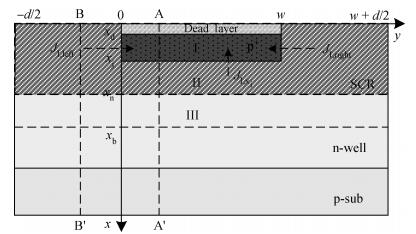
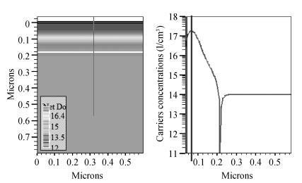
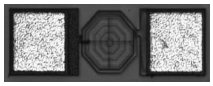
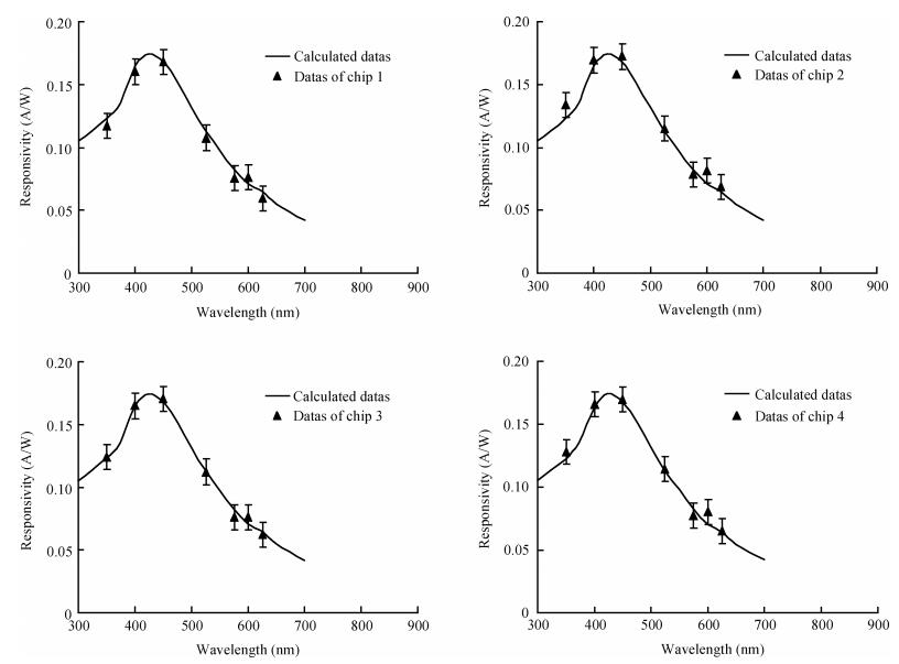
Table 1. Essential physical parameters used with the two-dimensional model

|
Table 2. Comparisons of simulation results and silicon test results

|
| [1] |
Charbon E. Towards large scale CMOS single-photon detector arrays for lab-on-chip applications. J Phys D:Appl Phys, 2008, 41(9):1
|
| [2] |
Chang Y W, Yu P C, Huang Y T, et al. A CMOS-compatible optical biosensing system based on visible absorption spectroscopy. Proceedings of IEEE Int Conf Electron Devices and Solid-State Circuits, Tainan, 2007
|
| [3] |
Pepin C M, Dautet H, Bergeron M, et al. New UV-enhanced, ultra-low noise silicon avalanche photodiode for radiation detection and medical imaging. Proceedings of Nuclear Science Symposium Conference Record (NSS/MIC), Knoxville, TN, 2010
|
| [4] |
Pauchard A, Besse P A, Popovic R S. A silicon blue/UV selective stripe-shaped photodiode. Sens Actuators, 1999, 76(1-3):172 doi: 10.1016/S0924-4247(99)00006-0
|
| [5] |
Ghazi A, Zimmermann H A, Seegebrecht P. CMOS photodiode with enhanced responsivity for the UV/blue spectral range. IEEE Trans Electron Devices, 2002, 49(7):1124 doi: 10.1109/TED.2002.1013266
|
| [6] |
Pauchard A, Rochas A, Randjelovic Z, et al. Ultraviolet avalanche photodiode in CMOS technology. Proceedings in IEDM Tech Dig, San Francisco CA, USA, 2000
|
| [7] |
Chang Y W, Huang Y T. The ring-shaped CMOS-based phototransistor with high responsivity for the UV/blue spectral range. IEEE Photonics Technol Lett, 2009, 21(13):899 doi: 10.1109/LPT.2009.2020176
|
| [8] |
Li Guike, Feng Peng, Wu Nanjian. A novel monolithic ultraviolet image sensor based on a standard CMOS process. Journal of Semiconductors, 2011, 32(10):105008 doi: 10.1088/1674-4926/32/10/105008
|
| [9] |
Esmaeili-Rad M R, Papadopoulos N P, Bauza M, et al. Blue-light-sensitive phototransistor for indirect X-ray image sensors. IEEE Electron Device Lett, 2012, 33(4):567 doi: 10.1109/LED.2012.2185676
|
| [10] |
Anderson B L, Anderson R L. Fundamentals of semiconductor devices (photocopy edition). 1st ed. Beijing:Tsinghua University Press, 2006
|
| [11] |
Jellison G E Jr. Optical functions of silicon determined by two-channel polarization modulation ellipsometry. Opt Mater, 1992, 1(1):41 doi: 10.1016/0925-3467(92)90015-F
|
| [12] |
Chen Bin, Yang Yintang, Li Yuejin, et al. Simulation and optimization of a 6H-SiC metal-semiconductor-metal ultraviolet photodetector. Journal of Semiconductors, 2010, 31(6):064010 doi: 10.1088/1674-4926/31/6/064010
|
| [13] |
Chen O C, Liu W J, Dai L K, et al. Extended one-dimensional analysis to effectively derive quantum efficiency of various CMOS photodiodes. IEEE Trans Electron Devices, 2007, 54(10):2659 doi: 10.1109/TED.2007.904989
|
| [14] |
Chen Yiren, Song Hang, Li Dabing, et al. GaN-based MSM photovoltaic ultraviolet detector structure modeling and its simulation. Journal of Semiconductors, 2011, 32(3):034005 doi: 10.1088/1674-4926/32/3/034005
|
| [15] |
Hamady S O S. A simulation of doping and trap effects on the spectral response of AlGaN ultraviolet detectors. Journal of Semiconductors, 2012, 33(3):034002 doi: 10.1088/1674-4926/33/3/034002
|
| [16] |
Chen Bin, Yang Yintang, Chai Changchun, et al. Two-dimensional numerical computation of the structure-dependent spectral response in a 4H-SiC metal-semiconductor-metal ultraviolet photodetector with consideration of reflection and absorption on contact electrodes. Journal of Semiconductors, 2011, 32(8):084001 doi: 10.1088/1674-4926/32/8/084001
|
| [17] |
Zabrodsky V V, Aruev P N, Sukhanov V L, et al. Silicon precision detectors for near IR, visible, UV, XUV and soft X-ray spectral range. Structure, 2010, 3(4):8
|
| [18] |
Chen W, Carini G, Keister J, et al. Development of the thin-junction detector. Proceedings in IEEE Nuclear Science Symposium Conference Record, San Diego CA, USA, 2006
|


Article views: 2618 Times PDF downloads: 15 Times Cited by: 0 Times
Received: 07 January 2014 Revised: 10 April 2014 Online: Published: 01 September 2014
| Citation: |
Changping Chen, Manfang Tian, Zhenyu Jiang, Xiangliang Jin, Jun Luo. Improved two-dimensional responsivity physical model of a CMOS UV and blue-extended photodiode[J]. Journal of Semiconductors, 2014, 35(9): 094009. doi: 10.1088/1674-4926/35/9/094009
****
C P Chen, M F Tian, Z Y Jiang, X L Jin, J Luo. Improved two-dimensional responsivity physical model of a CMOS UV and blue-extended photodiode[J]. J. Semicond., 2014, 35(9): 094009. doi: 10.1088/1674-4926/35/9/094009.

|
| [1] |
Charbon E. Towards large scale CMOS single-photon detector arrays for lab-on-chip applications. J Phys D:Appl Phys, 2008, 41(9):1
|
| [2] |
Chang Y W, Yu P C, Huang Y T, et al. A CMOS-compatible optical biosensing system based on visible absorption spectroscopy. Proceedings of IEEE Int Conf Electron Devices and Solid-State Circuits, Tainan, 2007
|
| [3] |
Pepin C M, Dautet H, Bergeron M, et al. New UV-enhanced, ultra-low noise silicon avalanche photodiode for radiation detection and medical imaging. Proceedings of Nuclear Science Symposium Conference Record (NSS/MIC), Knoxville, TN, 2010
|
| [4] |
Pauchard A, Besse P A, Popovic R S. A silicon blue/UV selective stripe-shaped photodiode. Sens Actuators, 1999, 76(1-3):172 doi: 10.1016/S0924-4247(99)00006-0
|
| [5] |
Ghazi A, Zimmermann H A, Seegebrecht P. CMOS photodiode with enhanced responsivity for the UV/blue spectral range. IEEE Trans Electron Devices, 2002, 49(7):1124 doi: 10.1109/TED.2002.1013266
|
| [6] |
Pauchard A, Rochas A, Randjelovic Z, et al. Ultraviolet avalanche photodiode in CMOS technology. Proceedings in IEDM Tech Dig, San Francisco CA, USA, 2000
|
| [7] |
Chang Y W, Huang Y T. The ring-shaped CMOS-based phototransistor with high responsivity for the UV/blue spectral range. IEEE Photonics Technol Lett, 2009, 21(13):899 doi: 10.1109/LPT.2009.2020176
|
| [8] |
Li Guike, Feng Peng, Wu Nanjian. A novel monolithic ultraviolet image sensor based on a standard CMOS process. Journal of Semiconductors, 2011, 32(10):105008 doi: 10.1088/1674-4926/32/10/105008
|
| [9] |
Esmaeili-Rad M R, Papadopoulos N P, Bauza M, et al. Blue-light-sensitive phototransistor for indirect X-ray image sensors. IEEE Electron Device Lett, 2012, 33(4):567 doi: 10.1109/LED.2012.2185676
|
| [10] |
Anderson B L, Anderson R L. Fundamentals of semiconductor devices (photocopy edition). 1st ed. Beijing:Tsinghua University Press, 2006
|
| [11] |
Jellison G E Jr. Optical functions of silicon determined by two-channel polarization modulation ellipsometry. Opt Mater, 1992, 1(1):41 doi: 10.1016/0925-3467(92)90015-F
|
| [12] |
Chen Bin, Yang Yintang, Li Yuejin, et al. Simulation and optimization of a 6H-SiC metal-semiconductor-metal ultraviolet photodetector. Journal of Semiconductors, 2010, 31(6):064010 doi: 10.1088/1674-4926/31/6/064010
|
| [13] |
Chen O C, Liu W J, Dai L K, et al. Extended one-dimensional analysis to effectively derive quantum efficiency of various CMOS photodiodes. IEEE Trans Electron Devices, 2007, 54(10):2659 doi: 10.1109/TED.2007.904989
|
| [14] |
Chen Yiren, Song Hang, Li Dabing, et al. GaN-based MSM photovoltaic ultraviolet detector structure modeling and its simulation. Journal of Semiconductors, 2011, 32(3):034005 doi: 10.1088/1674-4926/32/3/034005
|
| [15] |
Hamady S O S. A simulation of doping and trap effects on the spectral response of AlGaN ultraviolet detectors. Journal of Semiconductors, 2012, 33(3):034002 doi: 10.1088/1674-4926/33/3/034002
|
| [16] |
Chen Bin, Yang Yintang, Chai Changchun, et al. Two-dimensional numerical computation of the structure-dependent spectral response in a 4H-SiC metal-semiconductor-metal ultraviolet photodetector with consideration of reflection and absorption on contact electrodes. Journal of Semiconductors, 2011, 32(8):084001 doi: 10.1088/1674-4926/32/8/084001
|
| [17] |
Zabrodsky V V, Aruev P N, Sukhanov V L, et al. Silicon precision detectors for near IR, visible, UV, XUV and soft X-ray spectral range. Structure, 2010, 3(4):8
|
| [18] |
Chen W, Carini G, Keister J, et al. Development of the thin-junction detector. Proceedings in IEEE Nuclear Science Symposium Conference Record, San Diego CA, USA, 2006
|

 WeChat ID
Journal of Semiconductors © 2017 All Rights Reserved 京ICP备05085259号-2

 DownLoad: