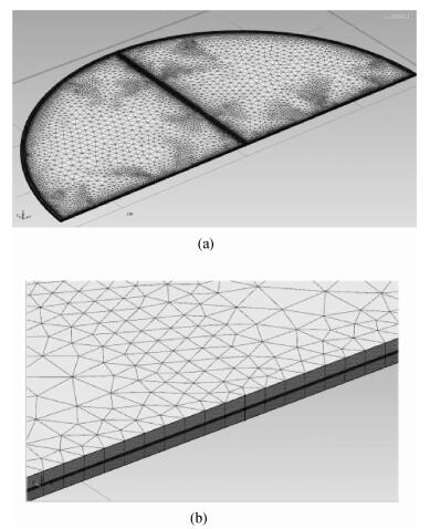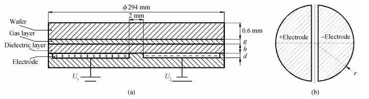
Fig. 1.
(a) Schematic illustration of ESC model. (b) Electrode pattern of two D-shape types
SEMICONDUCTOR DEVICES
Xingkuo Wang1, Jia Cheng2, , Kesheng Wang2, 3, Yiyong Yang1, Yuchun Sun2, Minglu Cao2 and Linhong Ji2
Corresponding author: Cheng Jia, Email:chengjia@tsinghua.edu.cn
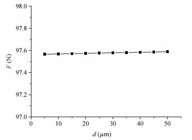
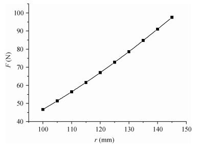
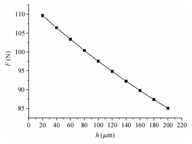
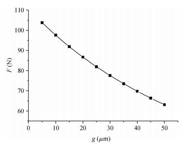
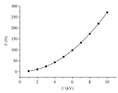
Abstract: As one of the core components of IC manufacturing equipment, the electrostatic chuck (ESC) has been widely applied in semiconductor processing such as etching, PVD and CVD. The clamping force of the ESC is one of the most important technical indicators. A multi-physics simulation software COMSOL is used to analyze the factors influencing the clamping force. The curves between the clamping force and the main parameters such as DC voltage, electrode thickness, electrode radius, dielectric thickness and helium gap are obtained. Moreover, the effects of these factors on the clamping force are investigated by means of orthogonal experiments. The results show that the factors can be ranked in order of voltage, electrode radius, helium gap and dielectric thickness according to their importance, which may offer certain reference for the design of ESCs.
Keywords: electrostatic chuck, clamping force, COMSOL simulation, orthogonal experiment
| [1] |
Asano K, Hatakeyama F, Yatsuzuka K. Fundamental study of an electrostatic chuck for silicon wafer handling. IEEE Trans Industry Applications, 2002, 38(3):840 doi: 10.1109/TIA.2002.1003438
|
| [2] |
Field J. Electrostatic wafer clamping for next-generation manufacturing. Solid State Technol, 1994, 37(9):91
|
| [3] |
Kanno S, Kato K, Yoshioka K, et al. Prediction of clamping pressure in a Johnsen-Rahbek-type electrostatic chuck based on circuit simulation. J Vac Sci Technol B, 2006, 24(1):216 doi: 10.1116/1.2151219
|
| [4] |
Wright D R, Chen L, Federlin P, et al. Manufacturing issues of electrostatic chucks. J Vac Sci Technol B, 1995, 13(4):1910 doi: 10.1116/1.588108
|
| [5] |
Watanabe T, Kitabayashi T, Nakayama C. Electrostatic charge-distribution in the dielectric layer of alumina electrostatic chuck. J Mater Sci, 1994, 29(13):3510 doi: 10.1007/BF00352057
|
| [6] |
Yatsuzuka K, Hatakeyama F, Asano K, et al. Fundamental characteristics of electrostatic wafer chuck with insulating sealant. IEEE Trans Industry Applications, 2000, 36(2):510 doi: 10.1109/28.833768
|
| [7] |
Yoo J, Choi J S, Hong S J, et al. Finite element analysis of the attractive force on a coulomb type electrostatic chuck. International Conference on Electrical Machines and Systems, 2007:642
|
| [8] |
Kalkowski G, Risse S, Harnisch G, et al. Electrostatic chucks for lithography applications. Microelectron Eng, 2001, 57/58:219 doi: 10.1016/S0167-9317(01)00519-6
|
| [9] |
Jeong K J, Spoutai S, Choi S H, et al. A study on the fabrication and characterization of alumina electrostatic chuck for silicon wafer processing. Third Russian-Korean International Symposium on Science and Technology, 1999:532
|
| [10] |
Daviet J F, Peccoud L, Mondon F. Electrostatic clamping applied to semiconductor plasma processing. 1. Theoretical modeling. J Electrochem Soc, 1993, 140(11):3245 doi: 10.1149/1.2221018
|
| [11] |
Cheng Jia, Zhu Yu, Ji Linhong. Modeling approach and analysis of the structural parameters of an inductively coupled plasma etcher based on a regression orthogonal design. Plasma Science and Technology, 2012, 14(12):1059 doi: 10.1088/1009-0630/14/12/05
|
Table 1. Constant parameters

|
Table 2. Variable Parameters

|
Table 3. Factor level table

|
Table 4. Orthogonal experiment table

|
Table 5. Results of orthogonal experiment

|
| [1] |
Asano K, Hatakeyama F, Yatsuzuka K. Fundamental study of an electrostatic chuck for silicon wafer handling. IEEE Trans Industry Applications, 2002, 38(3):840 doi: 10.1109/TIA.2002.1003438
|
| [2] |
Field J. Electrostatic wafer clamping for next-generation manufacturing. Solid State Technol, 1994, 37(9):91
|
| [3] |
Kanno S, Kato K, Yoshioka K, et al. Prediction of clamping pressure in a Johnsen-Rahbek-type electrostatic chuck based on circuit simulation. J Vac Sci Technol B, 2006, 24(1):216 doi: 10.1116/1.2151219
|
| [4] |
Wright D R, Chen L, Federlin P, et al. Manufacturing issues of electrostatic chucks. J Vac Sci Technol B, 1995, 13(4):1910 doi: 10.1116/1.588108
|
| [5] |
Watanabe T, Kitabayashi T, Nakayama C. Electrostatic charge-distribution in the dielectric layer of alumina electrostatic chuck. J Mater Sci, 1994, 29(13):3510 doi: 10.1007/BF00352057
|
| [6] |
Yatsuzuka K, Hatakeyama F, Asano K, et al. Fundamental characteristics of electrostatic wafer chuck with insulating sealant. IEEE Trans Industry Applications, 2000, 36(2):510 doi: 10.1109/28.833768
|
| [7] |
Yoo J, Choi J S, Hong S J, et al. Finite element analysis of the attractive force on a coulomb type electrostatic chuck. International Conference on Electrical Machines and Systems, 2007:642
|
| [8] |
Kalkowski G, Risse S, Harnisch G, et al. Electrostatic chucks for lithography applications. Microelectron Eng, 2001, 57/58:219 doi: 10.1016/S0167-9317(01)00519-6
|
| [9] |
Jeong K J, Spoutai S, Choi S H, et al. A study on the fabrication and characterization of alumina electrostatic chuck for silicon wafer processing. Third Russian-Korean International Symposium on Science and Technology, 1999:532
|
| [10] |
Daviet J F, Peccoud L, Mondon F. Electrostatic clamping applied to semiconductor plasma processing. 1. Theoretical modeling. J Electrochem Soc, 1993, 140(11):3245 doi: 10.1149/1.2221018
|
| [11] |
Cheng Jia, Zhu Yu, Ji Linhong. Modeling approach and analysis of the structural parameters of an inductively coupled plasma etcher based on a regression orthogonal design. Plasma Science and Technology, 2012, 14(12):1059 doi: 10.1088/1009-0630/14/12/05
|


Article views: 5559 Times PDF downloads: 288 Times Cited by: 0 Times
Received: 22 November 2013 Revised: 14 April 2014 Online: Published: 01 September 2014
| Citation: |
Xingkuo Wang, Jia Cheng, Kesheng Wang, Yiyong Yang, Yuchun Sun, Minglu Cao, Linhong Ji. Finite element analysis on factors influencing the clamping force in an electrostatic chuck[J]. Journal of Semiconductors, 2014, 35(9): 094011. doi: 10.1088/1674-4926/35/9/094011
****
X K Wang, J Cheng, K S Wang, Y Y Yang, Y C Sun, M L Cao, L H Ji. Finite element analysis on factors influencing the clamping force in an electrostatic chuck[J]. J. Semicond., 2014, 35(9): 094011. doi: 10.1088/1674-4926/35/9/094011.

|
| [1] |
Asano K, Hatakeyama F, Yatsuzuka K. Fundamental study of an electrostatic chuck for silicon wafer handling. IEEE Trans Industry Applications, 2002, 38(3):840 doi: 10.1109/TIA.2002.1003438
|
| [2] |
Field J. Electrostatic wafer clamping for next-generation manufacturing. Solid State Technol, 1994, 37(9):91
|
| [3] |
Kanno S, Kato K, Yoshioka K, et al. Prediction of clamping pressure in a Johnsen-Rahbek-type electrostatic chuck based on circuit simulation. J Vac Sci Technol B, 2006, 24(1):216 doi: 10.1116/1.2151219
|
| [4] |
Wright D R, Chen L, Federlin P, et al. Manufacturing issues of electrostatic chucks. J Vac Sci Technol B, 1995, 13(4):1910 doi: 10.1116/1.588108
|
| [5] |
Watanabe T, Kitabayashi T, Nakayama C. Electrostatic charge-distribution in the dielectric layer of alumina electrostatic chuck. J Mater Sci, 1994, 29(13):3510 doi: 10.1007/BF00352057
|
| [6] |
Yatsuzuka K, Hatakeyama F, Asano K, et al. Fundamental characteristics of electrostatic wafer chuck with insulating sealant. IEEE Trans Industry Applications, 2000, 36(2):510 doi: 10.1109/28.833768
|
| [7] |
Yoo J, Choi J S, Hong S J, et al. Finite element analysis of the attractive force on a coulomb type electrostatic chuck. International Conference on Electrical Machines and Systems, 2007:642
|
| [8] |
Kalkowski G, Risse S, Harnisch G, et al. Electrostatic chucks for lithography applications. Microelectron Eng, 2001, 57/58:219 doi: 10.1016/S0167-9317(01)00519-6
|
| [9] |
Jeong K J, Spoutai S, Choi S H, et al. A study on the fabrication and characterization of alumina electrostatic chuck for silicon wafer processing. Third Russian-Korean International Symposium on Science and Technology, 1999:532
|
| [10] |
Daviet J F, Peccoud L, Mondon F. Electrostatic clamping applied to semiconductor plasma processing. 1. Theoretical modeling. J Electrochem Soc, 1993, 140(11):3245 doi: 10.1149/1.2221018
|
| [11] |
Cheng Jia, Zhu Yu, Ji Linhong. Modeling approach and analysis of the structural parameters of an inductively coupled plasma etcher based on a regression orthogonal design. Plasma Science and Technology, 2012, 14(12):1059 doi: 10.1088/1009-0630/14/12/05
|

 WeChat ID
Journal of Semiconductors © 2017 All Rights Reserved 京ICP备05085259号-2

 DownLoad: