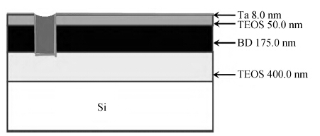
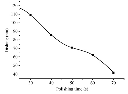
Fig. 1.
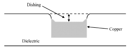
Schematic~diagram of dishing.
SEMICONDUCTOR TECHNOLOGY
Shiyan Fan1, 2, , Yuling Liu1, Ming Sun1, Jiying Tang1, Chenqi Yan1, Hailong Li1 and Shengli Wang1
Corresponding author: Shiyan Fan, E-mail: 494866895@qq.com
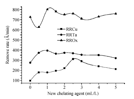
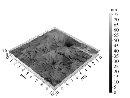
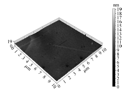
Abstract: To strengthen the device performance with the pattern wafer by enhancing the Cu polishing rate and improve the surface roughness with the Cu lines, a new weakly alkaline chelating agent with a barrier slurry is developed to meet the process demand of the advanced barrier chemical mechanical planarization (CMP). This new chelating agent has a stronger chelating ability and a lower pH value than the previous generation-FA/O I chelating agent researched before. Without an unstable oxidant agent added in the polishing slurry, it is difficult to enhance the copper polishing rate during the barrier CMP. The stronger chelating ability of the new chelating agent could increase the copper polishing rate along with controlling the Cu/Ta/TEOS removal rate selectivity to meet the requirements of the IC fabrication process. Thus it has solved the problem of excessive roughness due to the lower polishing rate, avoiding reducing the device performance with the pattern wafer. The new chelating agent with its lower pH value could make it possible to protect the low-k dielectric under the barrier layer from structurally breaking. The CMP experiment was performed on the 12 inch MIT 854 pattern wafers with the barrier slurry containing the new weakly alkaline chelating agent. By the DOE optimization, the results indicate that as the new chelating agent concentration in the slurry was up to 2.5 mL/L, the copper polishing rate is about 31.082 nm/min. Meanwhile, the wafer surface has a rather low roughness value of 0.693 nm (10 × 10 μm), the correction ability with the above slurry is adapted to the next generation barrier CMP and the k value of the low-k dielectric seems to have no k-shift. All the results presented show that the new weakly alkaline chelating agent with its superior performance can be used for the advanced barrier CMP.
Keywords: barrier CMP, chelating agent, polishing rate, surface roughness
| [1] | |
| [2] | |
| [3] | |
| [4] | |
| [5] | |
| [6] | |
| [7] | |
| [8] | |
| [9] | |
| [10] | |
| [11] | |
| [12] |
| [1] | |
| [2] | |
| [3] | |
| [4] | |
| [5] | |
| [6] | |
| [7] | |
| [8] | |
| [9] | |
| [10] | |
| [11] | |
| [12] |


Article views: 3049 Times PDF downloads: 43 Times Cited by: 0 Times
Received: 08 June 2014 Revised: Online: Published: 01 January 2015
| Citation: |
Shiyan Fan, Yuling Liu, Ming Sun, Jiying Tang, Chenqi Yan, Hailong Li, Shengli Wang. Next generation barrier CMP slurry with novel weakly alkaline chelating agent[J]. Journal of Semiconductors, 2015, 36(1): 016002. doi: 10.1088/1674-4926/36/1/016002
****
S Y Fan, Y L Liu, M Sun, J Y Tang, C Q Yan, H L Li, S L Wang. Next generation barrier CMP slurry with novel weakly alkaline chelating agent[J]. J. Semicond., 2015, 36(1): 016002. doi: 10.1088/1674-4926/36/1/016002.

|
| [1] | |
| [2] | |
| [3] | |
| [4] | |
| [5] | |
| [6] | |
| [7] | |
| [8] | |
| [9] | |
| [10] | |
| [11] | |
| [12] |

 WeChat ID
Journal of Semiconductors © 2017 All Rights Reserved 京ICP备05085259号-2

 DownLoad: