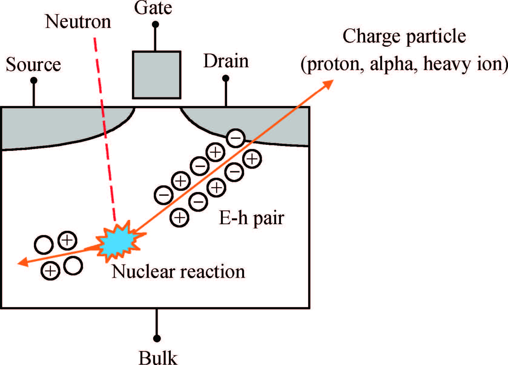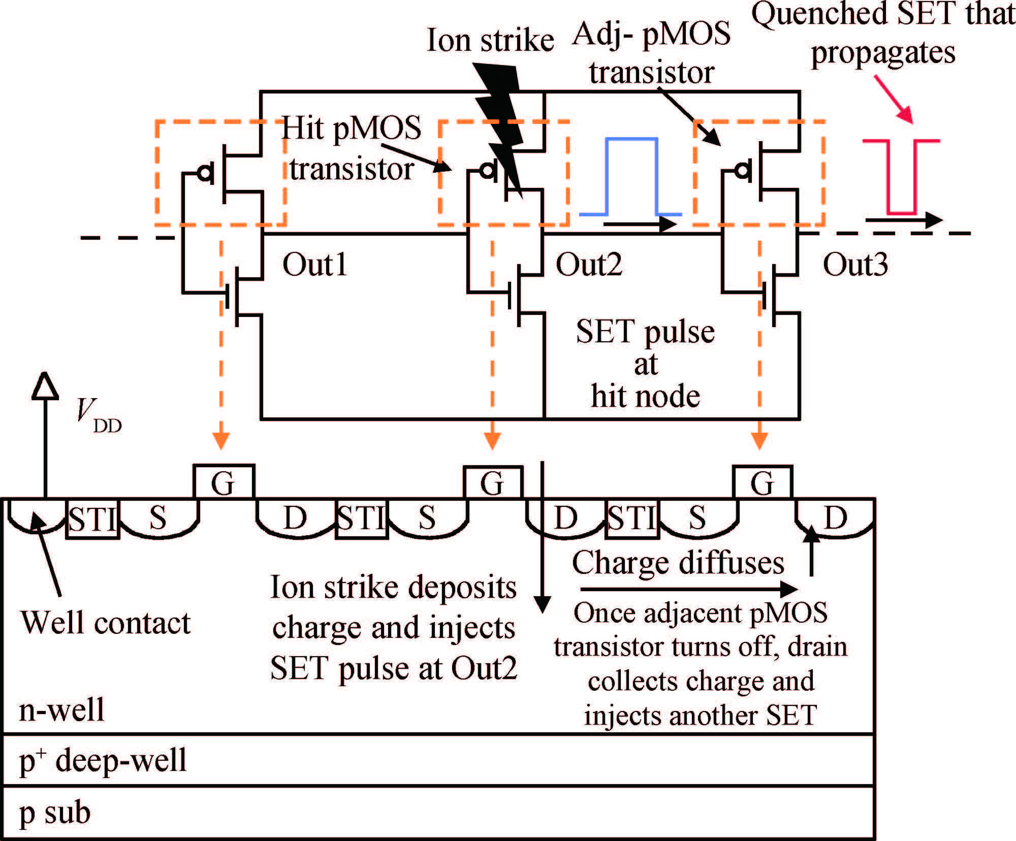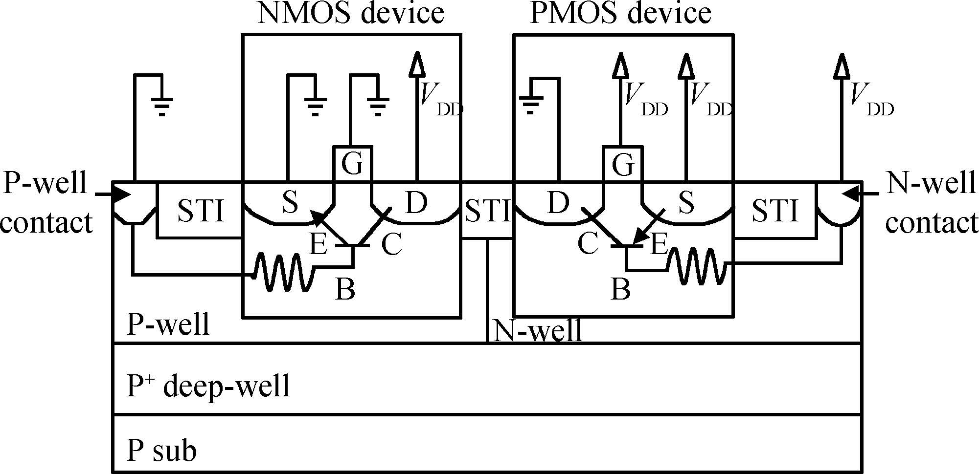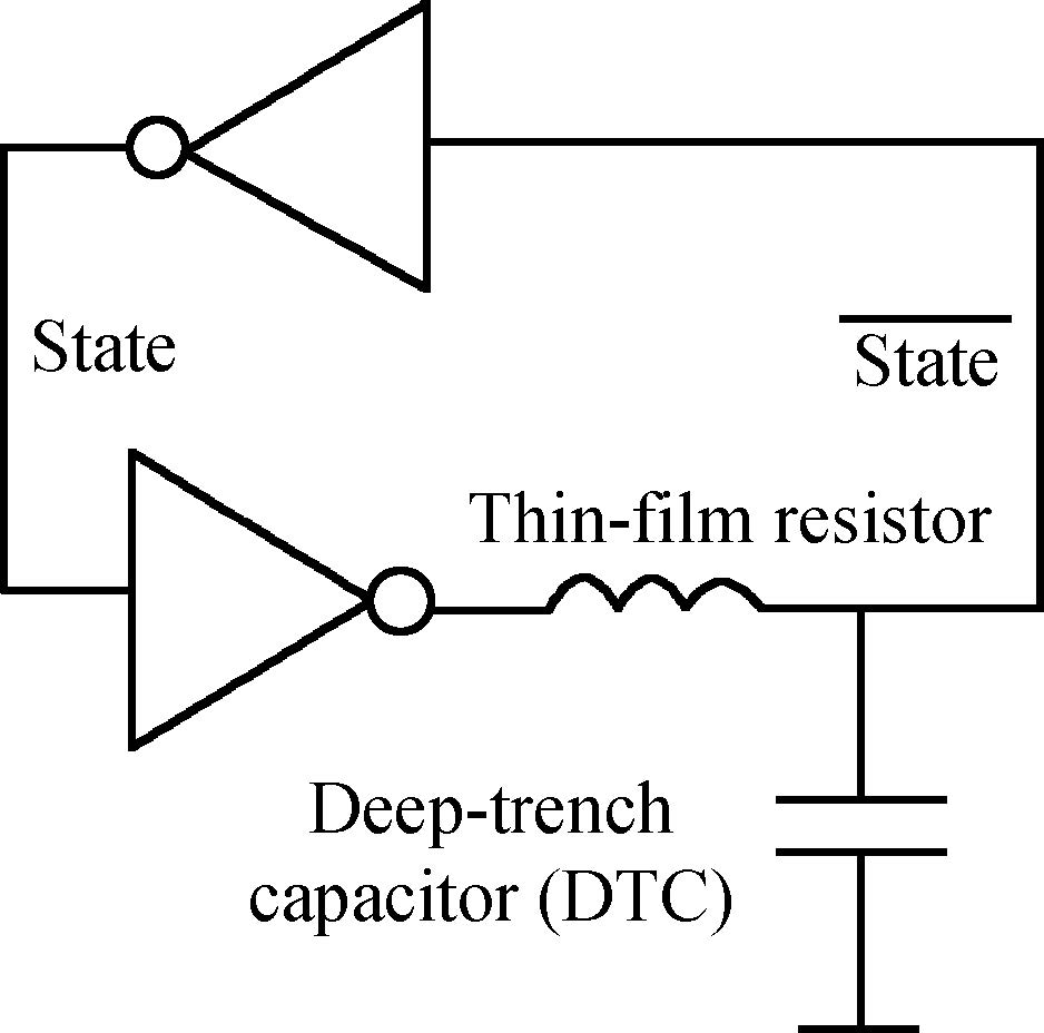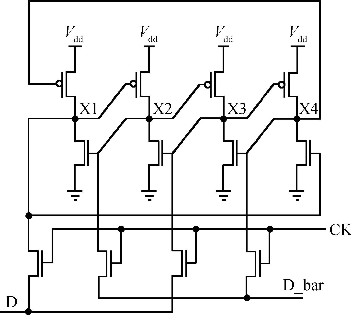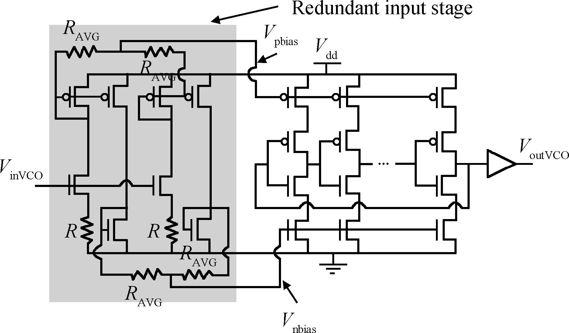
Fig. 1.
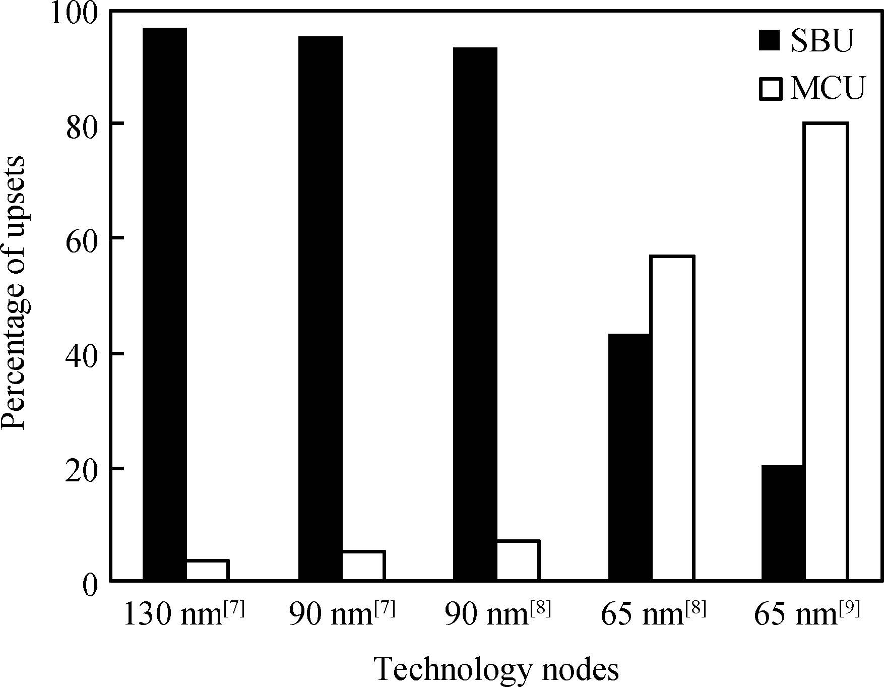
Percentage of SBU and MCU (130-65 nm).
INVITED REVIEW PAPERS
Yuanfu Zhao1, Suge Yue1, 2, Xinyuan Zhao1, , Shijin Lu1, Qiang Bian1, Liang Wang1 and Yongshu Sun1
Corresponding author: Zhao Xinyuan, Email: denniso@163.com
Abstract: As technology feature sizes decrease, single event upset (SEU), and single event transient (SET) dominate the radiation response of microcircuits. Multiple bit upset (MBU) (or multi cell upset) effects, digital single event transient (DSET) and analogue single event transient (ASET) caused serious problems for advanced integrated circuits (ICs) applied in a radiation environment and have become a pressing issue. To face this challenge, a lot of work has been put into the single event soft error mechanism and mitigation schemes. This paper presents a review of SEU and SET, including: a brief historical overview, which summarizes the historical development of the SEU and SET study since their first observation in the 1970's; effects prominent in advanced technology, which reviews the effects such as MBU, MSET as well as SET broadening and quenching with the influence of temperature, device structure etc.; the present understanding of single event soft error mechanisms, which review the basic mechanism of single event generation including various component of charge collection; and a discussion of various SEU and SET mitigation schemes divided as circuit hardening and layout hardening that could help the designer meet his goals.
Keywords: SET, SEU, MCU, advanced technology
| [1] | |
| [2] | |
| [3] | |
| [4] | |
| [5] | |
| [6] | |
| [7] | |
| [8] | |
| [9] | |
| [10] | |
| [11] | |
| [12] | |
| [13] | |
| [14] | |
| [15] | |
| [16] | |
| [17] | |
| [18] | |
| [19] | |
| [20] | |
| [21] | |
| [22] | |
| [23] | |
| [24] | |
| [25] | |
| [26] | |
| [27] | |
| [28] | |
| [29] | |
| [30] | |
| [31] | |
| [32] | |
| [33] | |
| [34] | |
| [35] | |
| [36] | |
| [37] | |
| [38] | |
| [39] | |
| [40] | |
| [41] | |
| [42] | |
| [43] | |
| [44] | |
| [45] | |
| [46] | |
| [47] | |
| [48] | |
| [49] | |
| [50] | |
| [51] | |
| [52] | |
| [53] | |
| [54] | |
| [55] | |
| [56] | |
| [57] | |
| [58] | |
| [59] | |
| [60] | |
| [61] | |
| [62] | |
| [63] | |
| [64] | |
| [65] | |
| [66] | |
| [67] | |
| [68] | |
| [69] | |
| [70] | |
| [71] | |
| [72] | |
| [73] | |
| [74] | |
| [75] | |
| [76] | |
| [77] | |
| [78] | |
| [79] | |
| [80] | |
| [81] | |
| [82] | |
| [83] | |
| [84] | |
| [85] | |
| [86] | |
| [87] | |
| [88] | |
| [89] | |
| [90] | |
| [91] | |
| [92] | |
| [93] | |
| [94] | |
| [95] | |
| [96] | |
| [97] | |
| [98] | |
| [99] | |
| [100] | |
| [101] | |
| [102] | |
| [103] | |
| [104] | |
| [105] | |
| [106] | |
| [107] | |
| [108] | |
| [109] | |
| [110] | |
| [111] | |
| [112] | |
| [113] | |
| [114] | |
| [115] | |
| [116] | |
| [117] | |
| [118] | |
| [119] | |
| [120] | |
| [121] | |
| [122] | |
| [123] | |
| [124] | |
| [125] | |
| [126] | |
| [127] | |
| [128] | |
| [129] | |
| [130] | |
| [131] | |
| [132] | |
| [133] | |
| [134] | |
| [135] | |
| [136] | |
| [137] | |
| [138] | |
| [139] | |
| [140] | |
| [141] | |
| [142] | |
| [143] | |
| [144] | |
| [145] | |
| [146] | |
| [147] | |
| [148] | |
| [149] | |
| [150] | |
| [151] | |
| [152] | |
| [153] | |
| [154] | |
| [155] | |
| [156] | |
| [157] |


Article views: 7215 Times PDF downloads: 157 Times Cited by: 0 Times
Received: 11 June 2015 Revised: Online: Published: 01 November 2015
| Citation: |
Yuanfu Zhao, Suge Yue, Xinyuan Zhao, Shijin Lu, Qiang Bian, Liang Wang, Yongshu Sun. Single event soft error in advanced integrated circuit[J]. Journal of Semiconductors, 2015, 36(11): 111001. doi: 10.1088/1674-4926/36/11/111001
****
Y F Zhao, S G Yue, X Y Zhao, S J Lu, Q Bian, L Wang, Y S Sun. Single event soft error in advanced integrated circuit[J]. J. Semicond., 2015, 36(11): 111001. doi: 10.1088/1674-4926/36/11/111001.

|
| [1] | |
| [2] | |
| [3] | |
| [4] | |
| [5] | |
| [6] | |
| [7] | |
| [8] | |
| [9] | |
| [10] | |
| [11] | |
| [12] | |
| [13] | |
| [14] | |
| [15] | |
| [16] | |
| [17] | |
| [18] | |
| [19] | |
| [20] | |
| [21] | |
| [22] | |
| [23] | |
| [24] | |
| [25] | |
| [26] | |
| [27] | |
| [28] | |
| [29] | |
| [30] | |
| [31] | |
| [32] | |
| [33] | |
| [34] | |
| [35] | |
| [36] | |
| [37] | |
| [38] | |
| [39] | |
| [40] | |
| [41] | |
| [42] | |
| [43] | |
| [44] | |
| [45] | |
| [46] | |
| [47] | |
| [48] | |
| [49] | |
| [50] | |
| [51] | |
| [52] | |
| [53] | |
| [54] | |
| [55] | |
| [56] | |
| [57] | |
| [58] | |
| [59] | |
| [60] | |
| [61] | |
| [62] | |
| [63] | |
| [64] | |
| [65] | |
| [66] | |
| [67] | |
| [68] | |
| [69] | |
| [70] | |
| [71] | |
| [72] | |
| [73] | |
| [74] | |
| [75] | |
| [76] | |
| [77] | |
| [78] | |
| [79] | |
| [80] | |
| [81] | |
| [82] | |
| [83] | |
| [84] | |
| [85] | |
| [86] | |
| [87] | |
| [88] | |
| [89] | |
| [90] | |
| [91] | |
| [92] | |
| [93] | |
| [94] | |
| [95] | |
| [96] | |
| [97] | |
| [98] | |
| [99] | |
| [100] | |
| [101] | |
| [102] | |
| [103] | |
| [104] | |
| [105] | |
| [106] | |
| [107] | |
| [108] | |
| [109] | |
| [110] | |
| [111] | |
| [112] | |
| [113] | |
| [114] | |
| [115] | |
| [116] | |
| [117] | |
| [118] | |
| [119] | |
| [120] | |
| [121] | |
| [122] | |
| [123] | |
| [124] | |
| [125] | |
| [126] | |
| [127] | |
| [128] | |
| [129] | |
| [130] | |
| [131] | |
| [132] | |
| [133] | |
| [134] | |
| [135] | |
| [136] | |
| [137] | |
| [138] | |
| [139] | |
| [140] | |
| [141] | |
| [142] | |
| [143] | |
| [144] | |
| [145] | |
| [146] | |
| [147] | |
| [148] | |
| [149] | |
| [150] | |
| [151] | |
| [152] | |
| [153] | |
| [154] | |
| [155] | |
| [156] | |
| [157] |

 WeChat ID
Journal of Semiconductors © 2017 All Rights Reserved 京ICP备05085259号-2

 DownLoad: