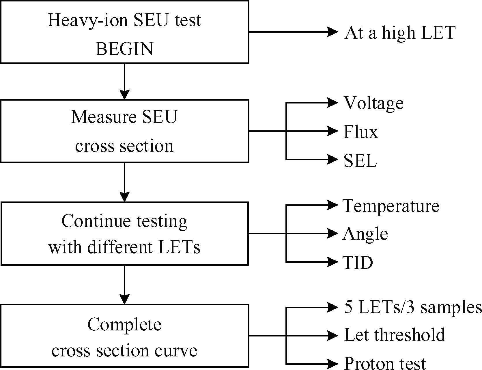
Processing math: 100%
J. Semicond. > 2015, Volume 36 > Issue 11 > 115002

SEMICONDUCTOR INTEGRATED CIRCUITS

The single-event effect evaluation technology for nano integrated circuits

Hongchao Zheng1, , Yuanfu Zhao1, Suge Yue1, 2, Long Fan1, Shougang Du1, Maoxin Chen1 and Chunqing Yu1

+ Author Affiliations

 Corresponding author: Zheng Hongchao, Email: hongchao_zheng@163.com

DOI: 10.1088/1674-4926/36/11/115002

PDF

Abstract: Single-event effects of nano scale integrated circuits are investigated. Evaluation methods for single-event transients, single-event upsets, and single-event functional interrupts in nano circuits are summarized and classified in detail. The difficulties in SEE testing are discussed as well as the development direction of test technology, with emphasis placed on the experimental evaluation of a nano circuit under heavy ion, proton, and laser irradiation. The conclusions in this paper are based on many years of testing at accelerator facilities and our present understanding of the mechanisms for SEEs, which have been well verified experimentally.

Key words: single-event effectheavy ion testradiation evaluation method

With the progress of semiconductor technology,the probability of single-event transients (SETs) and single-event upsets (SEUs) in nanometer-scale integrated circuits has increased. The critical charge threshold for single event effects (SEEs) is reduced,while the probability of single-event-induced charge sharing has increased due to the reduction of cell area. This has led to a new class of SEE called multi-bit/multi-cell upset (MBU/MCU)[1].

Therefore,the evaluation methods of single-event effects should increase in number for nanometer-scale circuits since the SEE sensitivity has increased.~Furthermore,it is difficult to configure and test complex circuits such as a mixed-signal system on a chip (SOC) with tens of millions of logic gates.

Novel circuit structures of a design for test (DFT) nature have been investigated and designed for the SEE evaluation of various circuit modules. Novel evaluation methods of single event function interrupt (SEFI) in complex applications have also been explored,as well as high frequency and high speed online test technology. In this paper,the SEE evaluation technology of nanometer-scale circuits is divided into four parts: assessment standard,evaluation method,testing technology,and radiation testing.

Currently,the existing standards for single-event testing are ESCC-25100,MIL-STD750E,ASTM-F1192,JESD57,and JESD89[2, 3, 4, 5, 6]. A common feature of the above standards is that the operation procedure of single-event testing is described in detail and the number of samples in heavy-ion radiation,ion energy,dose rate,total ionizing dose,and other requirements are clearly defined. The standards are suitable for evaluating a circuit (such as SRAM and A) for a single function or structure and for radiation tests of a class of single-event effects (such as SEU and SEL).

However,the definition of the failure standards for mixed-signal,large-scale integrated circuits,is not given in these standards. The classification methods for error statistics and the traditional approach for evaluating the single-event effect index of sub-modules are not suitable for evaluating the single-event performance in all applications. Therefore,experimental schemes for each test program are customized.

There is no uniform standard specified in the functional evaluation,so it is difficult to compare the performance of different circuits. Furthermore,the definitions of Weibull fitting,LET threshold,saturated cross section,and evaluation of error rates on-orbit are different across different standards. In the actual operation,there is a large statistical error for some definitions (e.g.,it is difficult to perform a Weibull fit on the actual test data if the fitting degree of the actual test data is not high,or the deviation for extracting the saturation section and LET threshold is great). In addition,there is no uniform prescription for the fitting software and error rate evaluation software in the standards,which causes deviation during the processing of test data.

In summary,the existing standard and specification system is not fully applicable to nanometer-scale radiation hardened ICs,and the single-event effects at all possible levels of nano technology need further study. In order to meet the requirements for single-event effects evaluation of nanometer IC,a more detailed evaluation method of the test needs to be developed on the basis of the existing standard and specification.

The test flow for heavy-ion-induced SEUs is shown in Figure1 [1]. The first test should be performed at a high LET in order to establish limits for the basic cross section range of the device under test (DUT). In the measurement of the SEU cross section,the bias voltage is chosen according to the circuit technology types (such as minimum voltage of standard bulk-silicon devices) to ensure that the DUT operates under the worst-case conditions. The particle fluencies should reach 1 × 107 cm2 or the number of upsets achieved should be 100. The fluence should be increased to 5 × 107 cm2 in cases where there are no SEUs measured to determine the LET threshold of the DUT. The DUT current must be monitored in real time during the experiment to determine whether an SEL happens and the current suddenly increases and cannot recover. SEL evaluation should be performed under the worst-case condition of high temperature at 125 °,the highest LET,and the maximum bias voltage. The SEU data will be enhanced by changing ion types and LETs and repeating the experiment. Furthermore,angle tests at 30° and 45° can be carried out to obtain the MBU/MCU sensitivity of the DUT. It is worth mentioning that the irradiation angle of horizontal and vertical direction can have differing MBU/MCU sensitivity. The total ionizing dose of DUT should be calculated at the last stage of the experiment and should not exceed 80% of the DUT maximum TID to ensure that the DUT can work properly for accuracy of the SEU test. According to the specification,the test should include at least 5 different LETs and the number of samples should be 3 or more. The experiment test data are fitted to a Weibull curve to obtain the saturation error cross section and LET threshold. The LET threshold is defined as the maximum LET at which no SEUs are detected,while another definition is the LET value of the 1% (or 10%) of the saturation error cross section on the Weibull curve. Proton SEE testing is suggested when the LET threshold of the DUT used on the LEO track is less than 40 MeVcm2/mg and especially if the LET threshold is less than 15 MeVcm2/mg. Proton tests are generally performed below 200 MeV,and the test procedure and method are the same as with heavy-ions,except that the metric used is not LET but MeV.

Figure  1.  Test flow of heavy-ion SEUs.

When high-energy particles pass through the critical regions of a phase-locked loop (PLL) circuit,the ion strike deposits energy and generates electron-hole pairs. These generated charge carriers can then be collected at the device terminals,leading to a transient current pulse on the struck node. The current pulses have a negative impact on the function of the PLL and can disrupt the system. A PLL system consists of many sub-circuits,so there are many sensitive nodes in a single PLL circuit. However,not all nodes sensitive to ion strikes will cause a serious impact on the output of the PLL[2].

The research for single-event effects in single function/structure circuits (such as SRAM,FLASH,ADDA,FPGA,and CDC) is relatively mature internationally. Based on the fact that the types of SEEs indifferent circuits have been thoroughly studied,the SEE test schedules for SEU,SET,SEFI,SEL,SEB,and SEGR effects are well-established. When the technology is scaled to the nanometer level,the single-event evaluation method for a single function/structure of the circuit is still applicable,but the LET threshold of circuits is lower. Therefore,the number of single-event effects will be higher. For a variety of functions/structure of nano-scale complex mixed-signal integrated circuits (such as SOC,ASIC)[7, 8, 9],a system can feature large-scale,multi-module,complex-functions for the integration of the analog/digital IP,PLL,high-speed interface,memory units (DFF/SRAM/CACHE/REG),and other circuit structures. This type of circuit tends to have a variety of single-event effects and different programs show different sensitivity to single-event effects. In recent years,the study of SEE evaluation methods on complex,mixed-signal circuits can be divided into two ways:

(1) The test method of SEU/SET is executed based on the built-in-self-test. Figure2 shows the SEU/SET test system diagram.

Figure  2.  SEU/SET test system diagram of nano-scale IC.

This method is mainly used to evaluate the characteristics of SET and SEU inside sensitive cells by sub-module. The built-in-self-test usually contains a scan chain test method,which strings the internal trigger as a chain [10, 11],and the SET and SEU occurring in flip-flops can be evaluated through real-time statistics from the output errors. In order to ensure the accuracy of SET tests[12, 13],the focus of current study is on improving the clock tree structure of the scan chain,which improves the operating frequency of the scan chain toward the maximum operating frequency of the circuit. A memory built-in-self-test (MBIST) method[14] using MARCH algorithms to write/read all the RAM cells traversing the entire address and the number of errors,which is shown in the forms of pulse,is counted automatically. The focus of the current study is to locate the address where SEU occurs,in order to distinguish between the SBU (single-bit upsets) and MBU (multi-bit upsets); the method of capturing SET by pulse width detection circuit is to connect the output of combinational logic to a custom latch chain. When an SET occurs in the combinational logic circuit,it is transmitted to the latch chain with a delay function. Based on the output value of the latch,the pulse width of SET can be estimated and the statistics of the number of SET can be obtained.

The method for the read and return instructions of register (REG)/cache is to compile program instructions[15]. Fixed data is written to register and cache,and then read back in real time during irradiation to determine if SEUs occur. In the end,a statistical number of SEUs is obtained. The evaluation of a single module with one SEE can be easily achieved by the built-in-self-test described above and then the intrinsic sensitivity of each individual memory cell can be determined.

(2) The evaluation method for the target circuit in the application state.

It has been proposed that the usage of internal resources is determined by the software executed on the target circuit[16, 17]. The SEE sensitivity of complex,large scale integrated circuits varies greatly across different test programs and different operating modes. All these phenomena can be due to the impact of the duty cycle of the program. The duty cycle is the percentage of time that the resource is active. The usages of the functional units are different in the implementation of the application test programs but are less than 100%. The SEUs that occur in unused registers and memory will have no effect on the device. In order to evaluate the SEE sensitivity of devices overall,the discrepancy of single-event effects sensitivity caused by different test programs is considered. An evaluation method to predict the applied cross section of complex integrated circuits under different test programs is determined,which is based on the duty cycle. Different test programs call for different resources at different times. Through the design of different test programs,the instructions for each functional unit are separately controlled by the test programs. By combining the intrinsic cross section and the duty cycle,the applied cross section under different test programs can be predicted. Further,the intrinsic cross section of each functional unit can be determined by the test results of SEE under different test programs. Therefore,the error rate of the target circuit under any test program can be obtained. The test mode which generated the largest error rate is the worst-case test mode. The evaluation method of single-event effects under a certain application is illustrated in Figure3.

Figure  3.  The evaluation method of single event effects under a certain application.

During the evaluation of single-event effects,two effects between functional interrupt and instantaneous functional error should be distinguished. The former refers to an interruption that occurs due to the program runaway,and an external reset is needed to recover; the latter refers to an instantaneous functional error which can resume normal operation automatically after a period of abnormal operation of the circuit. Both of the two belong to the single-event functional error but have differing degrees of impact. The latter can be corrected by programming a detection mechanism,or operation errors can be avoided by regular updates. Therefore,the statistics of these two phenomena require their respective tests to be done separately. When measuring the indicators of a single-event functional error in a circuit,the total number of errors or interruptions should be chosen according to the application requirements.

Based on the evaluation method of duty cycle,the functional evaluation of a CPU with PERM and TOWER programs is carried out to get the single event cross section under different applications,which is compared with the results of heavy-ion irradiation. The results of Cl and Ti ions are shown in Table1,in which the duty cycle is equal to the application cross section divided by the intrinsic cross section. It can be seen that the maximum deviation of the duty cycle is no more than 20%,which means the evaluation method of the duty cycle can be used effectively to evaluate the single-event cross section on complex large-scale integrated circuits under different applications.

Table  1.  Comparison of evaluation and experiment cross section results.
DownLoad: CSV  | Show Table

SEE experiments using heavy-ion accelerators generally require the development of a specialized SEE test system. The test system requires remote control and real-time data collection,and the test board size and the size of the test equipment is limited by the available space at the test site[17, 18, 19]. Therefore,the board-level embedded test system set up combined with small-scale measurement equipment,high speed data acquisition boards,and real-time data acquisition are used during experiments and data is stored in the control computer. The problems of the nano circuits test are shown in Figure4.

Figure  4.  The problems of nano circuits test.

Nanoscale digital VLSI circuits operating frequencies can reach 300 MHz or more. The data bus transfer is rated up to 400 Mbps and the number of test pins is over 400. The FPGA[7] and ARM-based embedded systems can only operate at a frequency of about 200 MHz when monitoring 100 pins. It is difficult to meet the multi-pin test,while maintaining high-speed control.

The hardware of the test system needs to focus on high-speed SEE error test technology and functional application test miniaturization technology. We can design and build a dedicated high-speed data acquisition card combining multiple systems into a hybrid test system. The FPGA-based multi-distribution mode test systems can also be applied. For a nano-circuits SEE test board,the requirements of anti-surge,ground bounce,and signal reflection of electromagnetic interference will be higher than micro-circuitry regardless of what kind of speed the test system is capable of. For the evaluation of the accuracy of single-particle test data results,signal lines of equal length and the opposite signal canceling interference methods need to be considered in order to avoid disturbance rejection caused by system abnormalities. Additionally,more high-speed ether net protocol needs to be developed because of the low transfer rate of the RS232/485 and the transmission distance limit of USB.

The signal will be affected by routing and layout in nano-scale circuits test board because of the signal arrival time inconsistency in each node and the reflected signal also reaching a node inconsistently,resulting in deterioration of signal quality. In general,the same number of multi-node branches can be controlled by star topology where signal transmission and reflection time delay are equal,which improves signal quality.

Power supply stability contributes to the increasingly-strict requirements of nano integrated circuits. The high-speed switching of circuit will inevitably produce power line voltage drop and electromagnetic interference with high-frequency components. Multiple methods are used to reduce the interference from the power supply system. First,the analog and digital power supply in a nano-circuit test board will be separated and connected together at the input to the power supply. Second,power lines will be kept in parallel with the ground line as far as possible,and at the same time,the power wire,ground wire,and the direction of data transmission must be in the same direction. Lastly,decoupling capacitors on one side of the power line will reduce the power line voltage fluctuations.

The higher demands for signal bandwidth would also be implemented in the nanoscale integrated circuits by utilizing the application of multi-channel transmission. The traditional point-to-point physical layer interface is clearly not suitable for increasing data transmission rates,due to its slow speed slow,power consumption,noise and other performance factors. With the development of LVDS technology,the above problems have been alleviated to some extent. LVDS can achieve low supply voltage and small voltage swing. For a difference signal bias of 1.2 V,a 400 mV swing can be achieved,and the most extreme contributions to noise are eliminated. LVDS can work under any power supply voltage,which can realize the stability of the power supply system. The power supply system can be changed little when the power supply voltage of the power supply voltage dependence is lower.

In the test system software design,the low-efficiency of the code in test vectors and state control should be resolved in order to ensure that SEE errors can be captured as quickly as possible by optimizing data storage structures and algorithms,control code size,and software delay. Then we can build a more complete state control to meet different application features and switching conditions at a variable configuration,and errors can be traced back to determine the time and area of SEE errors. Additionally the common state control and high-speed data transmission IP modules need to be established to meet the engineering requirements of different test circuits in the same platform control.

Three methods can be used for experimental investigation of SEEs: heavy-ion,proton and laser irradiation. Obviously particle irradiation tests require access to an adequate accelerator facility[20]. Laser testing at a pulsed laser facility can be used in SEE evaluation and sensitivity analysis without the need for access to expensive accelerator facilities.

Five ion species with varying LET would be used to evaluate the threshold of latch up and SEE saturation cross section in the heavy ion experiment,which requires a maximum ion LET of more than 75 MeVcm2/mg. The remaining four species determine the SEE threshold and Weibull curve. The LET threshold of nanoscale digital circuits would be 20 MeVcm2/mg or less. Since accelerators only generate specific LET values,in order to reduce the statistical error LET threshold value,one kind of ion LET with a threshold of more than 20 would be applied,with the remaining three species around the SEE threshold and having one ion species with LET below the SEE threshold.

The effective LET of energetic nuclear recoils induced by high-energy proton collisions in Si material is calculated to be about 15 MeVcm2/mg. Therefore,the proton SEE cannot be neglected for nano-circuits with the SEE threshold of no more than 15 MeVcm2/mg,especially for the crafts applied on the LEO orbit. Thus,the proton experiment should be considered for nano-circuits. The proton SEE test procedures and requirements are the same as in the heavy-ion experiment,except that the use of proton energy (MeV) is used as a metric instead of LET.

Habing first suggested that unfocused pulsed-laser light could be used to simulate electron and gamma-ray dose rate effects because both photons and particles ionize matter by liberating electrons from their constituent atoms[21]. Several groups in radiation research have focused on the issues of pulsed-laser induced SEEs. The increased use of the pulsed laser for SEE studies in recent years may be attributed to the confluence of several factors,including: the scaling of transistors to the point where they are becoming highly sensitive to SEEs,the availability of commercially manufactured picoseconds pulsed-lasers in the required wavelength range,the cost and limited time available at accelerators for testing,and the lack of spatial and temporal information obtained from broad-beam accelerator testing.

A popular time-domain,laser-based SEE research is presented in Reference [22],where the authors developed a time-domain,laser-based SEE test approach for nanoscale high-speed SerDes and phase lock loop (PLL) devices,which allows the oscilloscope and laser to each run at its own characteristic frequency. These approaches are applicable to other high-speed circuits including analog,mixed-signal,and digital. Advantages of the time-domain approach include the ability to characterize the full range of SETs,even varying program-to-program requirements,and to gather a data set that allows significant flexibility in terms of post-processing of the data beyond error identification and characterization. A space-domain,laser-based SEE research is presented in Reference [21],and is based on the advantages of the adjustability of the laser focal panel and the penetrability through the silicon substrate,and irradiation from the backside; the depth of sensitive volume in the longitudinal direction and the sensitive mapping in the transverse direction can be determined using this method. These methods can provide essential physical-structure-level information for layout-level radiation hardness and the establishment of SEE sensitive volume.

In summary,the single-event effect evaluation of a nano-radiation-hardened integrated circuit is a hot topic in the field of radiation effects and reliability of electronic devices. Nanoscale technology circuits present functional complexity and a diversity of single-event effects. Thus,further study of the radiation effects assessment methods is required,and enhancement of existing SEE test systems to solidify and unify the forms of verification is required in order to meet nano circuits radiation-hardened evaluation requirements.


[1]
[2]
[3]
[4]
[5]
[6]
[7]
[8]
[9]
[10]
[11]
[12]
[13]
[14]
[15]
[16]
[17]
[18]
[19]
[20]
[21]
[22]
Fig. 1.  Test flow of heavy-ion SEUs.

Fig. 2.  SEU/SET test system diagram of nano-scale IC.

Fig. 3.  The evaluation method of single event effects under a certain application.

Fig. 4.  The problems of nano circuits test.

Table 1.   Comparison of evaluation and experiment cross section results.

DownLoad: CSV
[1]
[2]
[3]
[4]
[5]
[6]
[7]
[8]
[9]
[10]
[11]
[12]
[13]
[14]
[15]
[16]
[17]
[18]
[19]
[20]
[21]
[22]
1

Reactive facet of carbon nitride single crystals

Kong Liu

Journal of Semiconductors, 2020, 41(9): 090202. doi: 10.1088/1674-4926/41/9/090202

2

Simulation study on single event burnout in linear doping buffer layer engineered power VDMOSFET

Jia Yunpeng, Su Hongyuan, Jin Rui, Hu Dongqing, Wu Yu, et al.

Journal of Semiconductors, 2016, 37(2): 024008. doi: 10.1088/1674-4926/37/2/024008

3

Effects of heavy ion irradiation on ultra-deep-submicron partially-depleted SOI devices

Weikang Wu, Xia An, Fei Tan, Hui Feng, Yehua Chen, et al.

Journal of Semiconductors, 2015, 36(11): 114004. doi: 10.1088/1674-4926/36/11/114004

4

Experimental research of heavy ion and proton induced single event effects for a Bi-CMOS technology DC/DC converter

Anlin He, Gang Guo, Shuting Shi, Dongjun Shen, Jiancheng Liu, et al.

Journal of Semiconductors, 2015, 36(11): 115010. doi: 10.1088/1674-4926/36/11/115010

5

Single event soft error in advanced integrated circuit

Yuanfu Zhao, Suge Yue, Xinyuan Zhao, Shijin Lu, Qiang Bian, et al.

Journal of Semiconductors, 2015, 36(11): 111001. doi: 10.1088/1674-4926/36/11/111001

6

Impacts of test factors on heavy ion single event multiple-cell upsets in nanometer-scale SRAM

Yinhong Luo, Fengqi Zhang, Hongxia Guo, Yao Xiao, Wen Zhao, et al.

Journal of Semiconductors, 2015, 36(11): 114009. doi: 10.1088/1674-4926/36/11/114009

7

Modeling and simulation of single-event effect in CMOS circuit

Suge Yue, Xiaolin Zhang, Yuanfu Zhao, Lin Liu

Journal of Semiconductors, 2015, 36(11): 111002. doi: 10.1088/1674-4926/36/11/111002

8

The effects of electron irradiation on the optical properties of the organic semiconductor polypyrrole

J. V. Thombare, M. C. Rath, S. H. Han, V. J. Fulari

Journal of Semiconductors, 2013, 34(9): 093001. doi: 10.1088/1674-4926/34/9/093001

9

Stacking fault energy in some single crystals

Aditya M.Vora

Journal of Semiconductors, 2012, 33(6): 062001. doi: 10.1088/1674-4926/33/6/062001

10

Atomic layer deposition of an Al2O3 dielectric on ultrathin graphite by using electron beam irradiation

Jiang Ran, Meng Lingguo, Zhang Xijian, Hyung-Suk Jung, Cheol Seong Hwang, et al.

Journal of Semiconductors, 2012, 33(9): 093004. doi: 10.1088/1674-4926/33/9/093004

11

Radiation effect on the optical and electrical properties of CdSe(In)/p-Si heterojunction photovoltaic solar cells

M. Ashry, S. Fares

Journal of Semiconductors, 2012, 33(10): 102001. doi: 10.1088/1674-4926/33/10/102001

12

Effect of rhenium doping on various physical properties of single crystals of MoSe2

Mihir M. Vora, Aditya M. Vora

Journal of Semiconductors, 2012, 33(1): 012001. doi: 10.1088/1674-4926/33/1/012001

13

A software solution to estimate the SEU-induced soft error rate for systems implemented on SRAM-based FPGAs

Wang Zhongming, Yao Zhibin, Guo Hongxia, Lü Min

Journal of Semiconductors, 2011, 32(5): 055008. doi: 10.1088/1674-4926/32/5/055008

14

Luminescence spectroscopy of ion implanted AlN bulk single crystal

Li Weiwei, Zhao Youwen, Dong Zhiyuan, Yang Jun, Hu Weijie, et al.

Journal of Semiconductors, 2009, 30(8): 083002. doi: 10.1088/1674-4926/30/8/083002

15

Thermal analysis and test for single concentrator solar cells

Cui Min, Chen Nuofu, Yang Xiaoli, Wang Yu, Bai Yiming, et al.

Journal of Semiconductors, 2009, 30(4): 044011. doi: 10.1088/1674-4926/30/4/044011

16

Modeling and analysis of single-event transients in charge pumps

Zhao Zhenyu, Li Junfeng, Zhang Minxuan, Li Shaoqing

Journal of Semiconductors, 2009, 30(5): 055006. doi: 10.1088/1674-4926/30/5/055006

17

A New Method to Investigate InGaAsP Single-Photon AvalancheDiodes Using a Digital Sampling Oscilloscope

Liu Wei, Yang Fuhua, Wu Meng

Chinese Journal of Semiconductors , 2006, 27(10): 1711-1716.

18

Ultra-Wideband Electromagnetic Radiation from GaAs Photoconductive Switches

Shi Wei,Jia Wanli, and Ji Weili

Chinese Journal of Semiconductors , 2005, 26(1): 11-15.

19

Influence of Floating Body Effect on Radiation Hardness of PD SOI nMOSFETs

Zhao Hongchen, Hai Chaohe, Han Zhengsheng,and Qian He

Chinese Journal of Semiconductors , 2005, 26(2): 234-237.

20

Design, Fabrication, and Testing of Single-Side Alignment of 16×0.8nm Arrayed Waveguide Grating

Li Jian, An Junming, Wang Hongjie, Xia Junlei, Hu Xiongwei, et al.

Chinese Journal of Semiconductors , 2005, 26(2): 254-257.

1. Yang, W., Li, Y., Guo, G. et al. System-on-Chip Single Event Effect hardening design and validation using proton irradiation. Nuclear Engineering and Technology, 2022. doi:10.1016/j.net.2022.10.034
2. Magisetty, R.P., Shukla, A., Kandasubramanian, B. Dielectric, Hydrophobic Investigation of ABS/NiFe2O4 Nanocomposites Fabricated by Atomized Spray Assisted and Solution Casted Techniques for Miniaturized Electronic Applications. Journal of Electronic Materials, 2018, 47(9): 5640-5656. doi:10.1007/s11664-018-6452-x
3. Pilia, R., Bascoul, G., Sanchez, K. et al. Single event transient acquisition and mapping for space device characterization. 2017.
4. Pilia, R., Bascoul, G., Sanchez, K. et al. Single Event Transient acquisition and mapping for space device Characterization. Microelectronics Reliability, 2016. doi:10.1016/j.microrel.2016.07.079
  • Search

    Advanced Search >>

    GET CITATION

    Hongchao Zheng, Yuanfu Zhao, Suge Yue, Long Fan, Shougang Du, Maoxin Chen, Chunqing Yu. The single-event effect evaluation technology for nano integrated circuits[J]. Journal of Semiconductors, 2015, 36(11): 115002. doi: 10.1088/1674-4926/36/11/115002
    H C Zheng, Y F Zhao, S G Yue, L Fan, S G Du, M X Chen, C Q Yu. The single-event effect evaluation technology for nano integrated circuits[J]. J. Semicond., 2015, 36(11): 115002. doi: 10.1088/1674-4926/36/11/115002.
    shu

    Export: BibTex EndNote

    Article Metrics

    Article views: 2464 Times PDF downloads: 20 Times Cited by: 4 Times

    History

    Received: 11 June 2015 Revised: Online: Published: 01 November 2015

    Catalog

      Email This Article

      User name:
      Email:*请输入正确邮箱
      Code:*验证码错误
      Hongchao Zheng, Yuanfu Zhao, Suge Yue, Long Fan, Shougang Du, Maoxin Chen, Chunqing Yu. The single-event effect evaluation technology for nano integrated circuits[J]. Journal of Semiconductors, 2015, 36(11): 115002. doi: 10.1088/1674-4926/36/11/115002 ****H C Zheng, Y F Zhao, S G Yue, L Fan, S G Du, M X Chen, C Q Yu. The single-event effect evaluation technology for nano integrated circuits[J]. J. Semicond., 2015, 36(11): 115002. doi: 10.1088/1674-4926/36/11/115002.
      Citation:
      Hongchao Zheng, Yuanfu Zhao, Suge Yue, Long Fan, Shougang Du, Maoxin Chen, Chunqing Yu. The single-event effect evaluation technology for nano integrated circuits[J]. Journal of Semiconductors, 2015, 36(11): 115002. doi: 10.1088/1674-4926/36/11/115002 ****
      H C Zheng, Y F Zhao, S G Yue, L Fan, S G Du, M X Chen, C Q Yu. The single-event effect evaluation technology for nano integrated circuits[J]. J. Semicond., 2015, 36(11): 115002. doi: 10.1088/1674-4926/36/11/115002.

      The single-event effect evaluation technology for nano integrated circuits

      DOI: 10.1088/1674-4926/36/11/115002
      More Information
      • Corresponding author: Zheng Hongchao, Email: hongchao_zheng@163.com
      • Received Date: 2015-06-11
      • Accepted Date: 2015-07-23
      • Published Date: 2015-01-25

      Catalog

        /

        DownLoad:  Full-Size Img  PowerPoint
        Return
        Return