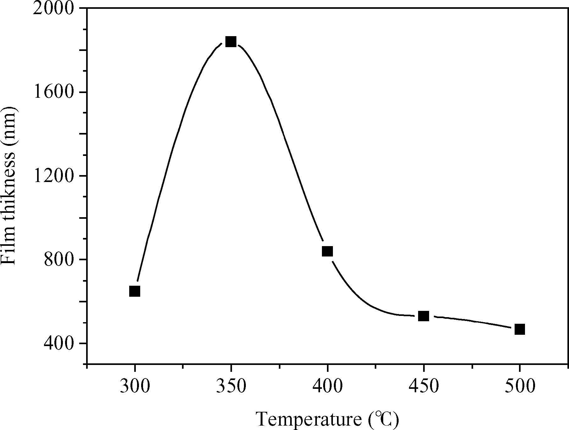
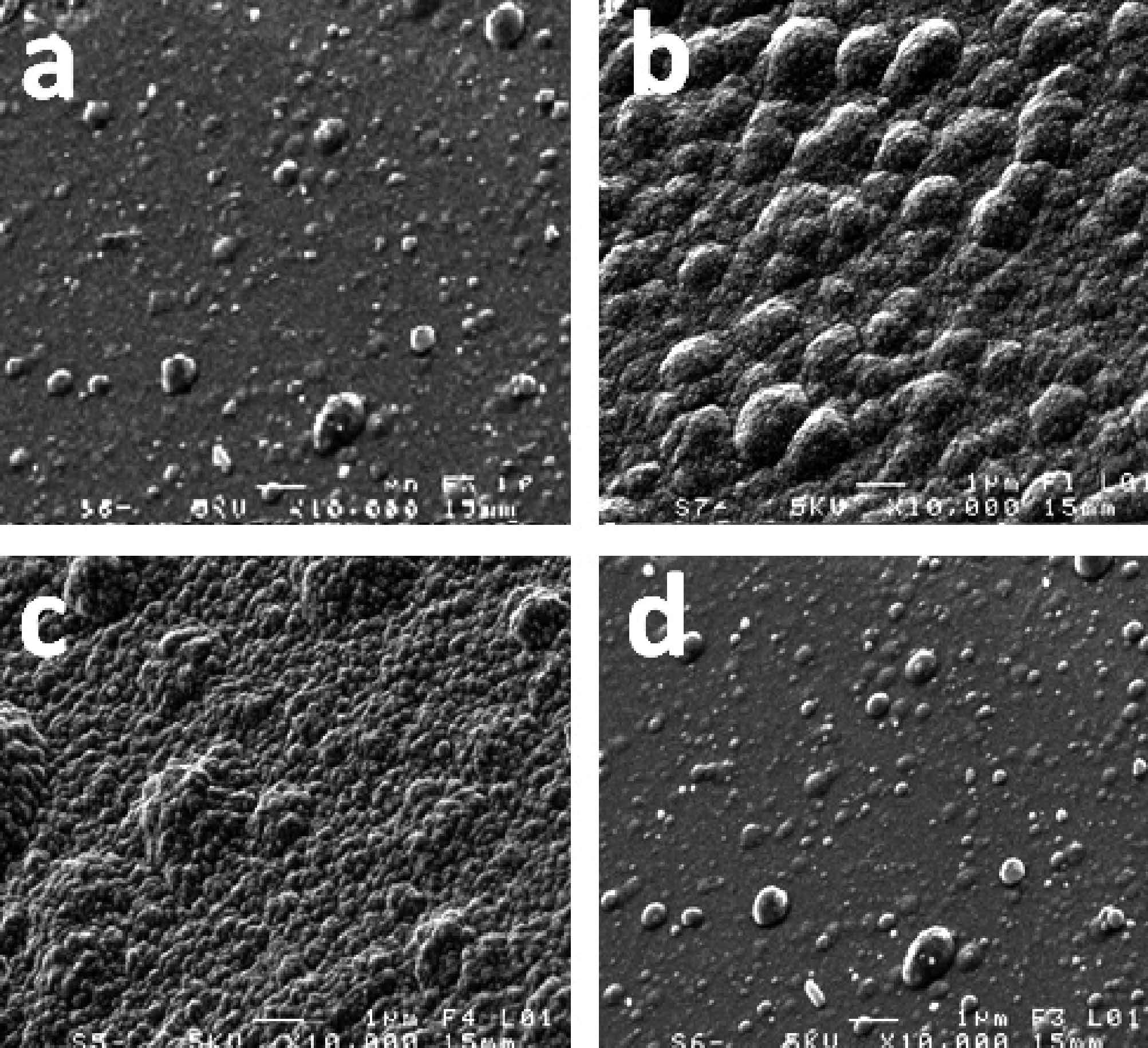
1. Introduction
Metal oxide semiconductors such as SnO2,In2O3,CdO and ZnO have been used in the opto-electronic devices mostly for flat panel displays,photovoltaic devices,gas sensors and heat reflecting mirrors because of their suitable band gaps of 2.8-4.2 eV,n-type conductivity and other useful characteristics[1]. Tin oxide thin films are transparent and conductive,and are particularly useful when good transparency in the visible range and good electrical conductivity are simultaneously required[2]. SnO2 films have high chemical stability and physical strength. SnO2 films can also be used in energy conversion systems. This material could find application in semiconductor electrodes for hydrogen based photo-electrochemical conversion and solar cells. SnO2 thin film can be prepared by a number of methods,such as CVD[3, 4],sputtering[5, 6],spray pyrolysis[7, 8],plasma and sol-gel methods[9],each of which had advantages and disadvantages. The preparation of SnO2 films has been well established by a spray ultrasonic technique. This technique is simple,inexpensive and permits easy deposition in the atmospheric condition. The optical and structural properties of spray deposited SnO2 films have also been well studied[10, 11],due to the greater interest of SnO2 thin films. The main accomplishment of this work is to characterize the SnO2 films (structural,optical and electrical characterisation) deposited by the spray ultrasonic process,and the film's properties dependence from the deposition conditions and the substrate temperatures. This is an important parameter for understanding the nature of thin film and its uses for required applications.
2. Experimental procedure
Tin oxide thin films were prepared by spraying an alcoholic solution that contains Tin Chloride dehydrate SnCl2-2H2O and CH4O onto glass substrates with deferent temperatures using ultrasonic spray process. Substrates were cleaned and degreased successively with Acetone,propanol,and distilled water. The films were deposited with a precursor molarity of 0.1 mol/L,and we have varied the temperature from 300 to 500 ℃ in atmospheric pressure. The films were characterized by means of structural,optical and electrical techniques. The film's thickness was calculated from the interference fringes obtained from transmittance spectra by the UV-VIS-NIR transmittance. The X-ray diffraction studies were carried out using a D8 ADVANCED BRUKER diffractometer with a copper anode having a wavelength λ = 1.5418Å; the crystallite sizes were estimated to study the effect of the temperature. The UV-VIS-NIR transmittance measurements were performed by using a PerkinElmer LAMBDA1050 UV/VIS/NIR spectrometer in the spectral range 300-1500 nm.
3. Results and discussion
3.1 Structural properties
The X-ray diffraction patterns for SnO2 films deposited at 300,350,400,450 and 500 ℃ are shown in Figure2. It can be found that films deposited at 300 ℃ were nearly amorphous whereas for higher temperatures,the amorphous background was diminished and diffraction peak (110) of standard SnO2 powder revealed for all samples as mentioned by other researchers[12, 13, 14, 15]. While the films deposited at higher temperatures exhibit five peaks. It is evident that the films deposited at 350,400,450 and 500 ℃ are polycrystalline in nature. In all films the half width of the Bragg peak decreases and displays gradual change in the preferred orientation from (101) to (200) plane with an increase in the substrate temperature from 350 to 500 ℃[16].
In order to determine the variation of the crystallite size with increasing substrate temperatures,the size of the crystallites oriented along the (101) plane is calculated using Scherrer's formula[ |
((1)) |
where D is the size of crystallite,Δθhkl the broadening of diffraction line measured at half its maximum intensity in radians and λ is the wavelength of X-rays (1.54 {\AA}). The calculated values of crystallite size are given in Figure3. It can be seen that the substrate's temperatures had an effective influence on the crystallite size,which increased from 21.9 to 72.2 nm. The growth in crystallite size is due to the fact by the increasing substrate's temperatures,which at higher than 300 ℃ during deposition was relatively high and enough to provide sufficient thermal energy for recrystallization. Hence,the crystallization process improved and the smaller crystallites agglomerated with increasing substrate temperature to cause a change in crystallite size distribution towards larger crystallites. This result is in agreement with those of other researchers[19, 20].
3.2 Optical properties
The optical transmission spectrum for SnO2 films deposited at 300,350,400,450 and 500 ℃ are shown in Figure~4,which shows the variation of transmittance with respect to the wavelength of SnO2 thin films deposited at various substrate temperatures. The average transmission in the visible region has been found to be ranging from 60% to 80% depending upon the substrate temperature. An increase in transmission is observed with an increase in temperature. At lower temperatures,at 350 ℃,a relatively lower transmission is due to the formation of milky films and that is because of incomplete decomposition of the sprayed droplets. In general,in the visible region of the spectrum,the transmission is high (high enough to observe interference fringes). It is due to the fact that the reflectivity is low and there is no (or less) absorption due to the transfer of electrons from the valence band to the conduction band owing to optical interference effects,so it is possible to maximize the transmission of thin film at a particular region of wavelengths[21].
We have used the pattern of transmission in the transparent region with successive minima and maxima to evaluate the thickness of the SnO2 films. The thickness d of the films can be calculated from the following equations[ |
((2)) |
The film's optical band gap has been determined on the basis of UV-VIS transmission measurements. The band gap (Eg) is determined by extrapolating the straight line portion of the plot to the energy axis. The intercept on the energy axis gives the value of band gap energy Eg for all the samples. The obtained optical band gap values lie in the range 3.92-3.98 eV. In Figure5 we have reported the variation of film thickness as a function of temperature. It shows that the film thickness decreases almost linearly with substrate temperature in the range 350-500 ℃,owing to the increased evaporation rate of the initial product with a rise in substrate temperature leading to the diminished mass transport towards the substrates[23]. At lower substrate temperatures 350-400 ℃,the temperature may not be sufficient to decompose the sprayed droplets of Sn2+ from the solution and this therefore,results in an increase of film thickness[24].
The variation of band gap Eg as a function of substrate temperature is shown in Figure6.
The obtained energy gap values are in good agreement with other literature reports[ |
((5)) |
3.3 Electrical properties
Electrical resistivity measurements have been carried out using the two-probe method. The variation of electrical resistivity of the SnO2 films as a function of temperature is shown in Figure7. It is observed that the resistivity of the films in the first decreases slowly with temperature in the range of 350-400~℃ and rapidly between 400 and 450 ℃. In fact,two competing processes of thermal excitation of electrons and oxygen adsorption occur simultaneously. The gradual reduction in film resistivity in the temperature range 350-400 ℃ is because the thermal excitation of electrons dominates over the oxygen adsorption process,while the sharp decrease in the film resistivity with temperature in the range 400-450 ℃ may be the result of improved adsorption of atmospheric oxygen at this range of temperatures. In fact this may be attributed to the adsorption of atmospheric oxygen on the film surface. In temperatures up to 450 ℃,the resistivity increases rapidly; it could be due to the grain boundaries effect that plays the role of traps for the electrons and consequently the film resistivity is increased. The variation of the resistivity can be also explained by the effect of films thickness. As reported in Figure5,the variation of the latter is opposite to the resistivity.
4. Conclusion
Highly transparent films of Tin oxide have been prepared by an ultrasonic spray CVD process. Films deposited at a temperature higher than 350 ℃ were identified as polycrystalline tin oxide films. The increase of temperature in the range of 350-500 ℃ improves the film's crystallinity and enhanced the crystallite size. The transmission in the visible and infrared regions of deposited films was found to be weakly affected by the temperature deposition between 300 and 500 ℃,in which range the film's transmittance exceeds 80%. The optical band gap values ranges between 3.92-3.98 eV for films deposited at different temperatures. The resistivity was found in the range of 0.016 to 0.04 Ω⋅cm. These films were suitable for low cost opto-electronic applications such as transparent conductive electrode,flat panel display and window filter in photovoltaic devices.