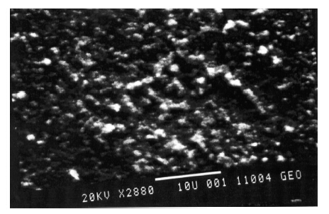
J. Semicond. > 2015, Volume 36 > Issue 3 > 033005

SEMICONDUCTOR MATERIALS

A comparison between different ohmic contacts for ZnO thin films

Shadia J. Ikhmayies1, Naseem M. Abu El-Haija2 and Riyad N. Ahmad-Bitar2

+ Author Affiliations

 Corresponding author: Shadia J. Ikhmayies, E-mail: shadia_ikhmayies@yahoo.com

DOI: 10.1088/1674-4926/36/3/033005

PDF

Abstract: There are several metals that form ohmic contacts for ZnO thin films, such as copper, aluminum and silver. The aim of this work is to make a comparison between these ohmic contacts. To achieve this purpose, polycrystalline ZnO thin films were prepared by the spray pyrolysis technique, and characterized by the I—V measurements at room temperature. Two strips of each metal were thermally evaporated on the surface of the film and measurements were first recorded in the dark and room light, then in the dark before and after annealing for Al, which was found to be the best in the set. Films with aluminum contacts gave the smallest resistivity, best ohmicity and they are slightly affected by light as required. On the other hand, copper was found to be the worst, and films with copper contacts gave the largest resistivity, worst ohmicity and they are the most affected by light. Annealing improved the aluminum contacts due to alloying and doping.

Key words: transparent conducting oxideohmic contactsannealingsolar cells

Transparent conducting oxides have attracted much attention in the growing market of flat panel displays and thin film solar cells[1]. Zinc oxide (ZnO) is considered a promising material for a variety of electronic and optoelectronic applications, including blue and UV solid-state lighting devices[2]. ZnO is a kind of non toxic[3, 4], low cost[5] and abundant[3, 6] material. With a wide direct bandgap of 3.37 eV[5, 7] it shows an excellent transparency for the entire visible spectrum[6]. In addition, ZnO devices are thermally stable[3], and do not suffer from dislocation degradation during operation[8]. It was found that ZnO thin films had a multitude of immensely important applications in electronic and optoelectronic devices such as transparent conductors, solar cell windows, gas sensors, surface acoustic wave (SAW) devices, and heat mirrors etc[3]. ZnO thin films can be prepared by different methods such as chemical solution deposition (CSD)[9], thermal evaporation[10], DC magnetron sputtering[11], spin coating[12], and the spray pyrolysis technique (SP)[13, 14, 15]. The spray pyrolysis used in this paper is a simple and low cost technique, which can intentionally and simply add the dopant into the precursor solution.

The electrical conductivity of ZnO is controlled by intrinsic defects, i.e., oxygen vacancies and/or zinc interstitials, which act as n-type donors[1]. It can be doped both by n- and p-type[9]. To get n-type ZnO, doping can be done with group III elements such as B, Al, Ga, or In. In annealing experiments up to 400 C, the conduction due to intrinsic defects is thermally unstable, whereas a better thermal stability is observed on layers doped extrinsically by indium or aluminum[1].

Measurements of the electrical properties of a semiconductor or an insulator are strongly affected by the contacts used. Hence, it is very important for choosing the suitable material and geometry of the contacts before measurements. The linear current-voltage characteristic, particularly at low voltages, is a criterion for the perfection of the contacts[13, 15, 16]. Ohmic contact resistance is strongly dependent on doping concentration because the tunneling process is more dominant at high doping levels[17]. The fabrication of ohmic contacts frequently includes a high temperature step, so that the deposited metals can either alloy with the semiconductor, or the high-temperature anneals reduce the unintentional barrier at the interface[13, 15, 18].

The literature reveals that different types of contacts were used for ZnO. Some researchers used a single element to form ohmic contacts, such as gold[1, 6, 19], aluminum[9, 20], indium[11], silver[3, 21] and Ti[9]. Among them, Ti was found to be a poor ohmic contact. Others used alloys for the same purpose, for example Al/Ti/Au[22, 23], and/or Ti/Au[20] contacts, which have the lowest contact resistivity between Ti, Al and Ti-Au.

Aluminum, silver and copper are used to make the contacts of ZnO thin films in this paper, where all of them are found to be ohmic. Our aim is to make a comparison between these ohmic contacts for ZnO thin films, and to find the best one in the electrical properties. The importance of this study lies in the use of ZnO as a transparent conducting oxide or a window material in heterojunction solar cells. For this purpose, it is important to investigate the electrical properties of this material, and good contacts are necessary for getting confidential results.

To produce ZnO thin films, a precursor solution is prepared by using 7.61 × 10³ mole of ZnCl2, dissolved in 300 mL of distilled water. To prevent the formation of Zn(OH)2, the PH of the solution was made equal to 3 by adding HCl. This solution was intermittently sprayed by using a home-made spray pyrolysis apparatus that was described in Reference [14]. The spraying was done vertically through a PVC nozzle on ordinary glass substrates placed on a heating block. The dimensions of the substrates are 2.5 × 6 × 0.1 cm3 and the substrate temperature is Ts = 450 C. Prior to deposition, the glass slides were cleaned by dipping in distilled water then by an ultrasonic cleaner, then soaked in methanol for 20-30 min, again soaked in distilled water and finally polished with lens papers. Nitrogen N2 was used as the carrier gas. The solution spray rate was in the range of 3-5 mL/min. The optimum carrier gas pressure for this rate of solution flow was around 5 kg/cm3. The nozzle to substrate distance was adjusted to get the largest uniform area about 30 cm in diameter.

The I-V measurements are taken in the dark and in room light at room temperature by a system that consists of a Keithley 2400 Source Meter capable of measuring 1011 A. Aluminum, silver, and copper are used as the contact materials for the films. Two strips of each of these metals are deposited on the surface of the film by thermal evaporation. The strips are of 1 cm length, 2 mm width, with a separation of 3 mm. A number of samples were annealed in nitrogen ambient at 250 C for 45 min after depositing the contacts on the surfaces of the films.

The transmittance of the films was measured in the wavelength range λ = 290-1100 nm by using a double beam Shimadzu UV 1601 (PC) spectrophotometer with respect to a piece of glass similar to the substrates. The minima and maxima in the transmittance curves are used to estimate the film thickness, where films of thickness between 300 and 600 nm are produced. The morphology of the films is observed with a scanning electron microscope (SEM) (LEITZ-AMR 1000A) and their structure is measured with an X-ray diffraction (XRD) (Philips PW1840) compact X-ray diffractometer system by using Cu Kα (λ = 1.5405 . The measurements are recorded at a diffraction angle 2θ in the range of 2- 81.

The set of films under study are all deposited from the same precursor solution with the same deposition parameters. The morphology of the films is explored by SEM observations, where Figure 1 displays the SEM image for one of the as-deposited films. As shown in Figure 1, the film appears to be polycrystalline and fully covered with material.

Figure  1.  SEM micrographs of one of the as-deposited ZnO thin films[24].

The structure is investigated with XRD, and Figure 2 depicts the diffractogram of a film, where the figure shows a hexagonal (wurtzite) structure. The strong narrow peak corresponds to the reflection from the (002) plane, and it confirms that the preferred growth direction is along the c-axis perpendicular to the substrate. In addition, there are five weaker diffraction peaks, which correspond to (100), (101), (102), (103) and (004), respectively. The Bragg equation (2dsinθ = nλ) was used to calculate interplanar distance d, where θ is Bragg's angle, n is the order which equals to 1, and λ = 1.5405 {\AA} is the wavelength of the incident X-ray (Cu Kα line). The interplanar distance d was found to be 0.261 nm, and the crystal lattice constant c was also calculated and found to be 0.522 nm. The grain size was estimated from the Scherrer formula and the line (002) in the XRD diffractogram.

d=λDcosθ,(1)
where d is the grain size, λ is the X-ray wavelength defined before, D is the angular line width of the half-maximum intensity, and θ is the Bragg angle defined before. The grain size calculated from Equation (1) is about 30 nm, which means that the particulates in the SEM image are aggregates, which consist of smaller crystallites.

Figure  2.  X-ray diffractogram of one of the as-deposited ZnO thin films.

The three different contacts: Al, Ag and Cu are deposited on the surfaces of the films by thermal evaporation-one type of contact on each film. Films with Al contacts are annealed in a nitrogen atmosphere for 45 min after depositing the contacts. Some of the criteria for the perfection of the contacts are linear current-voltage characteristics particularly at low voltages, and the absence of a photovoltaic effect[16]. The three aforementioned contacts are examined for achieving these criteria. For this purpose, the I-V measurements are recorded in the forward and reverse directions at room temperature in the dark and room light, and displayed in Figure 3. As shown in the figure, the relations are linear, which means that the three materials form ohmic contacts for ZnO.

Figure  3.  I-V plots and linear fits for ZnO thin films with different contacts. (a) In the dark. (b) In room light.

Linear fits which pass through the origin are performed, and the fit parameters R2, standard deviation SD and F are listed in Table 1. The resistance R is calculated from the slope of each straight line and used to find the resistivity ρ by using the relation R = ρL/A, where L is the length in the direction of the current and A is the cross-sectional area perpendicular to the current. The estimated values of R and ρ are listed in Table 2.

Table  1.  Fit parameters of the linear fits shown in Figure 3.
DownLoad: CSV  | Show Table
Table  2.  The values of resistance, resistivity and the ratio of the dark to the light resistivity for ZnO thin films with different contacts.
DownLoad: CSV  | Show Table

From Table 1 first, both in the dark and in room light, the highest slope is obtained by using Al contacts, while the lowest one by using Cu contacts. Second, the smallest standard deviation (SD) is got with Cu contacts, while the largest SD with Ag contacts. Third, in the dark and in room light, the best linearity, which is represented by the value of R2 is for Al contacts, which means that these contacts show the best ohmicity in the set under study. The largest F value is for Al contacts and the smallest one is for Ag contacts. Hence the best ohmic contacts from the set under study are Al contacts. These results can be explained in the light of the comparison between the electron affinity of ZnO, which is 4.1 eV[25] and the work functions of these contact materials, which are 4.74, 4.24, and 4.94 eV for Ag, Al and Cu respectively[26]. So, the closest work function to the electron affinity of ZnO is Al, while the farthest one is Cu. Hence the best ohmicity is Al, and the worst one is Cu, although all of them produced ohmic contacts because the values of the work functions are comparable to the electron affinity of ZnO.

From Table 2, the smallest resistance and resistivity are obtained with Al contacts, while the largest ones are with Cu contacts both in the dark and room light. As mentioned before, these results can be explained in terms of the electron affinity of ZnO and the work functions of the metals used as contacts. The work function of Al which equals 4.24 eV[26] is the closest to the electron affinity of ZnO which is 4.1 eV[25], while the work function of Cu, which is 4.94 eV[26], is the farthest.

The ratios of the dark resistivity ρdark to the light resistivity ρlight are shown in Table 2. The Cu contacts are the most affected by light (highest ρdark/ρlight), then the Ag contacts. These results can be interpreted in terms of the decrease in the barrier height caused by light. Al contacts are nearly unaffected by light, or approximately the photovoltaic effect on them is absent, which confirms that they are the best ohmic contacts in the set under study.

Annealing is known to improve the ohmic behavior of the contacts. Figure 4 displays the I-V plots for another two films with different thicknesses and Al contacts recorded in the dark before and after annealing. The relations are linear as before, and so linear fits that pass through the origin are performed. The fit parameters are listed in Table 3, and the estimated values of the resistance and resistivity and the ratios of the dark resistivity to the light resistivity are listed in Table 4. For both films there is a decrease in the resistivity after annealing. This is probably because more Al diffusion into the ZnO film occurs at high temperatures, which results in doping the region under the contacts and the formation of an alloy, and then a lower contact resistance. Comparing the resistivities of the thicker and thinner films after annealing, it is found that the resistivity of the thicker film is decreased by a factor of about 1.08, while that of the thinner one is decreased by a factor of about 2.44. Because grain size increases with film thickness[27, 28], the grains of the thicker film are larger, so a slight enlargement with annealing occurs and the decrease in resistivity is mainly due to the diffusion of aluminum into the film. In the case of the thinner film, the grain size is smaller, so more enlargement of the grains with annealing occurs, beside the diffusion of aluminum into the film. So, both of these factors contribute to decreasing the resistivity.

Figure  4.  The I-V plots and linear fits for two ZnO thin films with Al-contacts annealed in a nitrogen atmosphere at 250 C for 45 min. (a) Thickness = 600 nm. (b) Thickness = 370 nm.
Table  3.  Fit parameters of the linear fits shown in Figure 4.
DownLoad: CSV  | Show Table
Table  4.  The values of resistance, resistivity and the ratio of the as-deposited ρas to the annealed resistivity ρann for ZnO thin films with Al contacts in the dark.
DownLoad: CSV  | Show Table

Polycrystalline ZnO thin films were prepared by the spray pyrolysis technique on glass substrates. A comparison between three ohmic contacts for ZnO thin films was performed by the use of the I-V characterization. These contacts are aluminum, copper and silver. It is found that aluminum contacts are the best, because they resulted in the smallest resistivity, they contributed in doping through Al diffusion into the film, and they are less affected by light as required. Copper contacts are found to be the worst in the set, because they resulted in the largest resistivity and smallest ohmicity. Annealing improved the Al contact through improving the ohmicity, the interdiffusion, and alloying.

Acknowledgments

We want to thank Sameer Farrash at the University of Jordan for making the contacts by thermal evaporation. We also thank Marsil Imsais from the geology department in the University of Jordan for the XRD measurements and Mr. Khalil Tadros from the geology department in the University of Jordan for the SEM images.


[1]
[2]
[3]
[4]
[5]
[6]
[7]
[8]
[9]
[10]
[11]
[12]
[13]
[14]
[15]
[16]
[17]
[18]
[19]
[20]
[21]
[22]
[23]
[24]
[25]
[26]
[27]
[28]
Fig. 1.  SEM micrographs of one of the as-deposited ZnO thin films[24].

Fig. 2.  X-ray diffractogram of one of the as-deposited ZnO thin films.

Fig. 3.  I-V plots and linear fits for ZnO thin films with different contacts. (a) In the dark. (b) In room light.

Fig. 4.  The I-V plots and linear fits for two ZnO thin films with Al-contacts annealed in a nitrogen atmosphere at 250 C for 45 min. (a) Thickness = 600 nm. (b) Thickness = 370 nm.

DownLoad: CSV

Table 1.   Fit parameters of the linear fits shown in Figure 3.

DownLoad: CSV

Table 2.   The values of resistance, resistivity and the ratio of the dark to the light resistivity for ZnO thin films with different contacts.

DownLoad: CSV

Table 3.   Fit parameters of the linear fits shown in Figure 4.

DownLoad: CSV

Table 4.   The values of resistance, resistivity and the ratio of the as-deposited ρas to the annealed resistivity ρann for ZnO thin films with Al contacts in the dark.

DownLoad: CSV
[1]
[2]
[3]
[4]
[5]
[6]
[7]
[8]
[9]
[10]
[11]
[12]
[13]
[14]
[15]
[16]
[17]
[18]
[19]
[20]
[21]
[22]
[23]
[24]
[25]
[26]
[27]
[28]
1

Simulation and application of external quantum efficiency of solar cells based on spectroscopy

Guanlin Chen, Can Han, Lingling Yan, Yuelong Li, Ying Zhao, et al.

Journal of Semiconductors, 2019, 40(12): 122701. doi: 10.1088/1674-4926/40/12/122701

2

Surface passivation of perovskite film for efficient solar cells

Yang (Michael) Yang

Journal of Semiconductors, 2019, 40(4): 040204. doi: 10.1088/1674-4926/40/4/040204

3

Effect of annealing temperature on Ti/Al/Ni/Au ohmic contacts on undoped AlN films

Xuewei Li, Jicai Zhang, Maosong Sun, Binbin Ye, Jun Huang, et al.

Journal of Semiconductors, 2017, 38(11): 116002. doi: 10.1088/1674-4926/38/11/116002

4

Analysis of morphological, structural and electrical properties of annealed TiO2 nanowires deposited by GLAD technique

B. Shougaijam, R. Swain, C. Ngangbam, T.R. Lenka

Journal of Semiconductors, 2017, 38(5): 053001. doi: 10.1088/1674-4926/38/5/053001

5

Microwave annealing effects on ZnO films deposited by atomic layer deposition

Shirui Zhao, Yabin Dong, Mingyan Yu, Xiaolong Guo, Xinwei Xu, et al.

Journal of Semiconductors, 2014, 35(11): 112001. doi: 10.1088/1674-4926/35/11/112001

6

Theoretical investigation of some parameters into the behavior of quantum dot solar cells

A. Nasr, A. Aly

Journal of Semiconductors, 2014, 35(12): 124001. doi: 10.1088/1674-4926/35/12/124001

7

Improved memory performance of metal-oxide-nitride-oxide-silicon by annealing the SiO2 tunnel layer in different nitridation atmospheres

Meilin He, Jingping Xu, Jianxiong Chen, Lu Liu

Journal of Semiconductors, 2013, 34(11): 114005. doi: 10.1088/1674-4926/34/11/114005

8

Improving poor fill factors for solar cells via light-induced plating

Xing Zhao, Jia Rui, Ding Wuchang, Meng Yanlong, Jin Zhi, et al.

Journal of Semiconductors, 2012, 33(9): 094008. doi: 10.1088/1674-4926/33/9/094008

9

Influence of thermal treatment temperatures on CdTe nanocrystal films and photoelectric properties of ITO/CdTe/Al

Xu Wenqing, Qu Shengchun, Wang Kefan, Bi Yu, Liu Kong, et al.

Journal of Semiconductors, 2012, 33(9): 094002. doi: 10.1088/1674-4926/33/9/094002

10

Influence of absorber doping in a-SiC:H/a-Si:H/a-SiGe:H solar cells

Muhammad Nawaz, Ashfaq Ahmad

Journal of Semiconductors, 2012, 33(4): 042001. doi: 10.1088/1674-4926/33/4/042001

11

Nickel ohmic contacts of high-concentration P-implanted 4H-SiC

Liu Chunjuan, Liu Su, Feng Jingjing, Wu Rong

Journal of Semiconductors, 2012, 33(3): 036002. doi: 10.1088/1674-4926/33/3/036002

12

Analysis of the ohmic contacts of Ti/Al/Ni/Au to AlGaN/GaN HEMTs by the multi-step annealing process

Yan Wei, Zhang Renping, Du Yandong, Han Weihua, Yang Fuhua, et al.

Journal of Semiconductors, 2012, 33(6): 064005. doi: 10.1088/1674-4926/33/6/064005

13

Using I-V characteristics to investigate selected contacts for SnO2:F thin films

Shadia. J. Ikhmayies, Riyad N Ahmad-Bitar

Journal of Semiconductors, 2012, 33(8): 083001. doi: 10.1088/1674-4926/33/8/083001

14

As2S8 planar waveguide: refractive index changes following an annealing and irradiation and annealing cycle, and light propagation features

Zou Liner, Wang Gouri, Shen Yun, Chen Baoxue, Mamoru Iso, et al.

Journal of Semiconductors, 2011, 32(11): 112004. doi: 10.1088/1674-4926/32/11/112004

15

Effect of annealing process on the surface roughness in multiple Al implanted 4H-SiC

Wu Hailei, Sun Guosheng, Yang Ting, Yan Guoguo, Wang Lei, et al.

Journal of Semiconductors, 2011, 32(7): 072002. doi: 10.1088/1674-4926/32/7/072002

16

NiO removal of Ni/Au Ohmic contact to p-GaN after annealing

Lin Mengzhe, CaoQing, YanTingjing, ZhangShuming, ChenLianghui, et al.

Journal of Semiconductors, 2009, 30(2): 026001. doi: 10.1088/1674-4926/30/2/026001

17

Effect of chemical polish etching and post annealing on the performance of silicon heterojunction solar cells

Jiang Zhenyu, Dou Yuhua, Zhang Yu, Zhou Yuqin, Liu Fengzhen, et al.

Journal of Semiconductors, 2009, 30(8): 084010. doi: 10.1088/1674-4926/30/8/084010

18

External Quantum Efficiency of Quantum Well Solar Cells

Lou Chaogang, Yan Ting, Sun Qiang, Xu Jun, Zhang Xiaobing, et al.

Journal of Semiconductors, 2008, 29(11): 2088-2091.

19

High Temperature Characteristics of Ti/Al/Ni/Au Multilayer Ohmic Contact to n-GaN

Zhang Yuezong, Feng Shiwei, Zhang Gongchang, Wang Chengdong, Lü Changzhi, et al.

Chinese Journal of Semiconductors , 2007, 28(6): 984-988.

20

Effect of Surface-Covered Annealing on the Optical Properties of ZnO Films Grown by MOCVD

Wang Li, Pu Yong, Fang Wenqing, Mo Chunlan, Xiong Chuanbing, et al.

Chinese Journal of Semiconductors , 2003, 24(3): 409-412.

1. Allouche, N., Boudjema, B., Daira, R. et al. Morphological and optical characterization of spin-coated CuO nanostructured thin films doped with V, Na, Ba, and Er for enhanced CO2 sensing. Journal of Materials Research and Technology, 2025. doi:10.1016/j.jmrt.2025.01.048
2. Padha, B., Ahmed, Z., Dutta, S. et al. Ultrasensitive NO2 gas detection using ALD-grown ZnO-SiO2/Si thin film-based UV sensors. Journal of Alloys and Compounds, 2025. doi:10.1016/j.jallcom.2024.177673
3. Sirjani, S., Fattah, A., Haratizadeh, H. Effect of Electrode Shape on the Performance of ZnO-Based Ethanol Sensor. Journal of Sensors, 2024. doi:10.1155/2024/6696108
4. Mala, S., Latha, H.K.E., Udayakumar, A. Influence of post-deposition annealing temperature on structural and electrical properties of TiW contact thin films. Journal of the Korean Physical Society, 2023, 83(3): 194-199. doi:10.1007/s40042-023-00818-6
5. Mohaseba, M.A., Aboud, A.A. Effect of Pb doping onto physical properties of ZnO thin films deposited by AACVD. Journal of Materials Science: Materials in Electronics, 2023, 34(11): 941. doi:10.1007/s10854-023-10360-7
6. Abdel-Latif, M.K., Mobarak, M., Revaprasadu, N. et al. Effect of doping on the structural, optical and electrical properties of La-doped ZnO thin films. Journal of Materials Science: Materials in Electronics, 2023, 34(4): 254. doi:10.1007/s10854-022-09477-y
7. Li, Y., Nie, S., Huang, L. et al. Paper based self-powered UV photodiode: Enhancing photo-response with AZO back-field layer. Ceramics International, 2023, 49(3): 4831-4838. doi:10.1016/j.ceramint.2022.09.373
8. Soleimanpour, F., Darbari, S., Barahimi, B. et al. ZnO-Based Surface Acoustic Wave Droplet Sensor. 2023. doi:10.1109/IICM60532.2023.10443163
9. Ikhmayies, S.J.. Optical Parameters of ZnO Thin Films. Minerals, Metals and Materials Series, 2023. doi:10.1007/978-3-031-22576-5_4
10. Chatzigiannakis, G., Jaros, A., Leturcq, R. et al. Broadband wavelength-selective isotype heterojunction n+-ZnO/n-Si photodetector with variable polarity. Journal of Alloys and Compounds, 2022. doi:10.1016/j.jallcom.2022.163836
11. Nasirian, S., Hadizadeh, F. A cheap self-powered UV-photodetector based on layer-by-layer arrangement of polyaniline and ZnO. Polymer, 2022. doi:10.1016/j.polymer.2022.124699
12. Hadizadeh, F., Nasirian, S. Utilizing zinc oxide nanorods/polyaniline heterojunction as a flexible self-powered ultraviolet photodetector. Optical Materials, 2022. doi:10.1016/j.optmat.2021.111902
13. Labar, R., Kundu, T.K. Fabrication and Characterization of Back-to-Back Schottky Diode in Ni/ZnO/Ag Nanojunction. Journal of Electronic Materials, 2022, 51(1): 223-231. doi:10.1007/s11664-021-09280-1
14. Sun, Y., Zheng, Y., Wang, R. et al. Direct-current piezoelectric nanogenerator based on two-layer zinc oxide nanorod arrays with equal c-axis orientation for energy harvesting. Chemical Engineering Journal, 2021. doi:10.1016/j.cej.2021.131262
15. Saravanavel, G., Honnali, S.K., Lourdes, K.S. et al. Study on the thermoelectric properties of Al-ZnO thin-film stack fabricated by physical vapour deposition process for temperature sensing. Sensors and Actuators A: Physical, 2021. doi:10.1016/j.sna.2021.113097
16. El Haimeur, A., Slassi, A., Pershin, A. et al. Reducing p-type Schottky contact barrier in metal/ZnO heterostructure through Ni-doping. Applied Surface Science, 2021. doi:10.1016/j.apsusc.2021.149023
17. Chakraborty, M., Hashmi, M.S.J. Metal-Semiconductor Contacts in Industrial Applications and Processing. Encyclopedia of Smart Materials, 2021. doi:10.1016/B978-0-12-803581-8.10324-8
18. Al-Khalli, N., Aly Aboud, M.F., Bagabas, A.A. et al. Structural, optical, and electrical characteristics of thermal treated ZnO thin films deposited by RF sputtering on glass substrates. Materials Transactions, 2021, 62(7): 915-920. doi:10.2320/matertrans.MT-M2020350
19. Das, A., Chakraborty, S. Studies on al and Mg Co-Doped ZnO Thin Films Grown by Sol-Gel Technique. Lecture Notes in Networks and Systems, 2021. doi:10.1007/978-981-15-9433-5_42
20. Ikhmayies, S.J.. A Study of the Absorption Edge of ZnO Thin Films Prepared by the Spray Pyrolysis Method. Minerals, Metals and Materials Series, 2021. doi:10.1007/978-3-030-65493-1_8
21. Ikhmayies, S.J.. Spray-Deposited Coral-Like ZnO Micro/Nano Thin Films on Glass Substrates. JOM, 2021, 73(1): 356-363. doi:10.1007/s11837-020-04495-9
22. Rathod, K.N., Gadani, K., Dhruv, D. et al. Effect of oxygen vacancy gradient on ion-irradiated Ca-doped YMnO3thin films. Journal of Vacuum Science and Technology B, 2020, 38(6): 062208. doi:10.1116/6.0000507
23. Chatzigiannakis, G., Jaros, A., Leturcq, R. et al. Laser-Microstructured ZnO/p-Si Photodetector with Enhanced and Broadband Responsivity across the Ultraviolet-Visible-Near-Infrared Range. ACS Applied Electronic Materials, 2020, 2(9): 2819-2828. doi:10.1021/acsaelm.0c00492
24. Hasabeldaim, E.H.H., Ntwaeaborwa, O.M., Kroon, R.E. et al. Luminescence properties of Eu doped ZnO PLD thin films: The effect of oxygen partial pressure. Superlattices and Microstructures, 2020. doi:10.1016/j.spmi.2020.106432
25. Tappura, K., Juntunen, T., Jaakkola, K. et al. Large-area implementation and critical evaluation of the material and fabrication aspects of a thin-film thermoelectric generator based on aluminum-doped zinc oxide. Renewable Energy, 2020. doi:10.1016/j.renene.2019.09.093
26. Azizah, N., Muhammady, S., Purbayanto, M.A.K. et al. Influence of Al doping on the crystal structure, optical properties, and photodetecting performance of ZnO film. Progress in Natural Science: Materials International, 2020, 30(1): 28-34. doi:10.1016/j.pnsc.2020.01.006
27. Ikhmayies, S.J.. Synthesis of Flower-Like ZnO Micro/Nano Structures by the Spray Pyrolysis Technique. JOM, 2020, 72(2): 621-627. doi:10.1007/s11837-019-03952-4
28. Rathod, K.N., Gadani, K., Dhruv, D. et al. Investigations on the Electronic Excitations through Spectroscopic Measures for Resistive Switching Character of Manganite Thin Films. Physica Status Solidi (B) Basic Research, 2019, 256(12): 1900264. doi:10.1002/pssb.201900264
29. Yadav, A.B., Sannakashappanavar, B.S. True Ohmic contact on RF sputtered ZnO thin film by using the nonalloy Ti/Au metallization scheme. Journal of Alloys and Compounds, 2019. doi:10.1016/j.jallcom.2018.08.166
30. Ikhmayies, S.J., Juwhari, H.K., Lahlouh, B. Properties of ZnO Micro/nanostructures on aluminum substrates. Minerals, Metals and Materials Series, 2019. doi:10.1007/978-3-030-05749-7_24
31. Ikhmayies, S.J.. A comparison between ZnO hexagonal micro/nanoprisms deposited on aluminum and glass substrates. Minerals, Metals and Materials Series, 2019. doi:10.1007/978-3-030-05749-7_32
32. Rahman, M.S., Akter, M., Miah, S. et al. Influence of the Compositional Variation of ZnxCd1-xS (0 ≤ x ≤ 0.45) Buffer on Efficiency of Cu2ZnSnSe4 Solar Cell: A Simulation. 2018. doi:10.1109/INDICON45594.2018.8987129
33. Ismail, R.A., Al-Samarai, A.-M.E., Mohammed, W.M. Preparation of n-ZnO/p-Si heterojunction photodetector via rapid thermal oxidation technique: effect of oxidation time. Applied Physics A: Materials Science and Processing, 2018, 124(8): 527. doi:10.1007/s00339-018-1946-1
34. Ikhmayies, S.J.. ZnO thin films of flowered-fibrous micro/nanowebs on glass substrates using the spray pyrolysis method. Minerals, Metals and Materials Series, 2018. doi:10.1007/978-3-319-72484-3_23
35. Ikhmayies, S.J., Zbib, M.B. Spray Pyrolysis Synthesis of ZnO Micro/Nanorods on Glass Substrate. Journal of Electronic Materials, 2017, 46(10): 5629-5634. doi:10.1007/s11664-017-5629-z
36. Rathod, K.N., Dhruv, D., Gadani, K. et al. Comparison of charge transport studies of chemical solution and pulsed laser deposited manganite-based thin film devices. Applied Physics A: Materials Science and Processing, 2017, 123(8): 558. doi:10.1007/s00339-017-1172-2
37. Ikhmayies, S.J., Zbib, M.B. Synthesis of ZnO Hexagonal Micro Discs on Glass Substrates Using the Spray Pyrolysis Technique. Journal of Electronic Materials, 2017, 46(7): 3982-3986. doi:10.1007/s11664-017-5495-8
38. Abbass, A.E., Swart, H.C., Kroon, R.E. Non-plasmonic enhancement of the near band edge luminescence from ZnO using Ag nanoparticles. Journal of Luminescence, 2017. doi:10.1016/j.jlumin.2016.10.043
39. Ikhmayies, S.J.. Transparent conducting oxides for solar cell applications. Mediterranean Green Buildings and Renewable Energy: Selected Papers from the World Renewable Energy Network's Med Green Forum, 2017. doi:10.1007/978-3-319-30746-6_70
40. Benramache, S., Benhaoua, B. Influence of urbach energy with solution molarity on the electrical conductivity in undoped ZnO thin films. Journal of Nano- and Electronic Physics, 2016, 8(2): 02025. doi:10.21272/jnep.8(2).02025
  • Search

    Advanced Search >>

    GET CITATION

    Shadia J. Ikhmayies, Naseem M. Abu El-Haija, Riyad N. Ahmad-Bitar. A comparison between different ohmic contacts for ZnO thin films[J]. Journal of Semiconductors, 2015, 36(3): 033005. doi: 10.1088/1674-4926/36/3/033005
    S. J. Ikhmayies, N. M. A. El-Haija, R. N. Ahmad-Bitar. A comparison between different ohmic contacts for ZnO thin films[J]. J. Semicond., 2015, 36(3): 033005. doi:  10.1088/1674-4926/36/3/033005.
    shu

    Export: BibTex EndNote

    Article Metrics

    Article views: 3527 Times PDF downloads: 45 Times Cited by: 40 Times

    History

    Received: 10 July 2014 Revised: Online: Published: 01 March 2015

    Catalog

      Email This Article

      User name:
      Email:*请输入正确邮箱
      Code:*验证码错误
      Shadia J. Ikhmayies, Naseem M. Abu El-Haija, Riyad N. Ahmad-Bitar. A comparison between different ohmic contacts for ZnO thin films[J]. Journal of Semiconductors, 2015, 36(3): 033005. doi: 10.1088/1674-4926/36/3/033005 ****S. J. Ikhmayies, N. M. A. El-Haija, R. N. Ahmad-Bitar. A comparison between different ohmic contacts for ZnO thin films[J]. J. Semicond., 2015, 36(3): 033005. doi:  10.1088/1674-4926/36/3/033005.
      Citation:
      Shadia J. Ikhmayies, Naseem M. Abu El-Haija, Riyad N. Ahmad-Bitar. A comparison between different ohmic contacts for ZnO thin films[J]. Journal of Semiconductors, 2015, 36(3): 033005. doi: 10.1088/1674-4926/36/3/033005 ****
      S. J. Ikhmayies, N. M. A. El-Haija, R. N. Ahmad-Bitar. A comparison between different ohmic contacts for ZnO thin films[J]. J. Semicond., 2015, 36(3): 033005. doi:  10.1088/1674-4926/36/3/033005.

      A comparison between different ohmic contacts for ZnO thin films

      DOI: 10.1088/1674-4926/36/3/033005
      More Information
      • Corresponding author: E-mail: shadia_ikhmayies@yahoo.com
      • Received Date: 2014-07-10
      • Accepted Date: 2014-10-09
      • Published Date: 2015-01-25

      Catalog

        /

        DownLoad:  Full-Size Img  PowerPoint
        Return
        Return