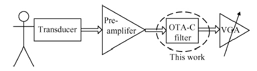
Fig. 1.
Analog frond-end circuit of ECG bio-telemetry monitoring system.
SEMICONDUCTOR INTEGRATED CIRCUITS
Jihai Duan, Chuang Lan, Weilin Xu and Baolin Wei
Corresponding author: Weilin Xu, E-mail: xwl@guet.edu.cn
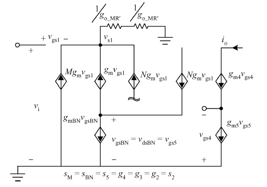
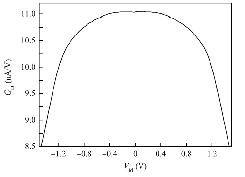
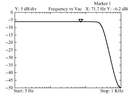
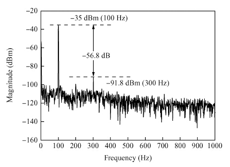
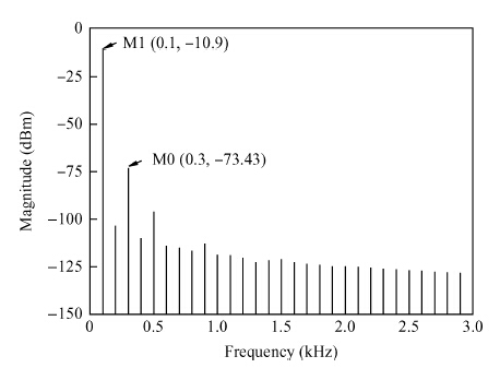
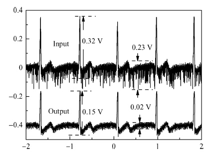
Abstract: A fifth order operational transconductance amplifier-C (OTA-C) Butterworth type low-pass filter with highly linear range and less passband attenuation is presented for wearable bio-telemetry monitoring applications in a UWB wireless body area network. The source degeneration structure applied in typical small transconductance circuit is improved to provide a highly linear range for the OTA-C filter. Moreover, to reduce the passband attenuation of the filter, a cascode structure is employed as the output stage of the OTA. The OTA-based circuit is operated in weak inversion due to strict power limitation in the biomedical chip. The filter is fabricated in a SMIC 0.18-μ m CMOS process. The measured results for the filter have shown a passband gain of -6.2 dB, while the -3-dB frequency is around 276 Hz. For the 0.8 VPP sinusoidal input at 100 Hz, a total harmonic distortion (THD) of -56.8 dB is obtained. An electrocardiogram signal with noise interference is fed into this chip to validate the function of the designed filter.
Keywords: ECG signal, fully differential OTA-C filter, highly linear range, less passband attenuation
| [1] | |
| [2] | |
| [3] | |
| [4] | |
| [5] | |
| [6] | |
| [7] | |
| [8] | |
| [9] | |
| [10] | |
| [11] | |
| [12] | |
| [13] | |
| [14] |
| [1] | |
| [2] | |
| [3] | |
| [4] | |
| [5] | |
| [6] | |
| [7] | |
| [8] | |
| [9] | |
| [10] | |
| [11] | |
| [12] | |
| [13] | |
| [14] |


Article views: 4178 Times PDF downloads: 89 Times Cited by: 0 Times
Received: 05 October 2014 Revised: Online: Published: 01 May 2015
| Citation: |
Jihai Duan, Chuang Lan, Weilin Xu, Baolin Wei. An OTA-C filter for ECG acquisition systems with highly linear range and less passband attenuation[J]. Journal of Semiconductors, 2015, 36(5): 055006. doi: 10.1088/1674-4926/36/5/055006
****
J H Duan, C Lan, W L Xu, B L Wei. An OTA-C filter for ECG acquisition systems with highly linear range and less passband attenuation[J]. J. Semicond., 2015, 36(5): 055006. doi: 10.1088/1674-4926/36/5/055006.

|
| [1] | |
| [2] | |
| [3] | |
| [4] | |
| [5] | |
| [6] | |
| [7] | |
| [8] | |
| [9] | |
| [10] | |
| [11] | |
| [12] | |
| [13] | |
| [14] |

 WeChat ID
Journal of Semiconductors © 2017 All Rights Reserved 京ICP备05085259号-2

 DownLoad: