


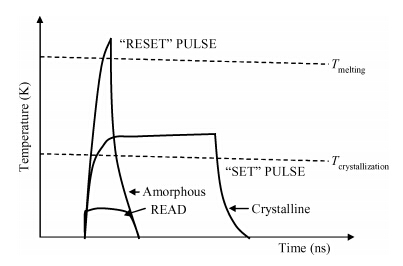
Fig. 1.
Schematic diagram showing temperature versus time graphs for reset and set pulses during programming of a PCM cell.
SEMICONDUCTOR MATERIALS
Joshua M. Kundu, Patrick M. Karimi and Walter K. Njoroge
Corresponding author: Joshua M. Kundu, Email: mrjkmasinde@gmail.com
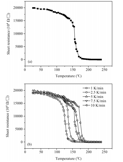
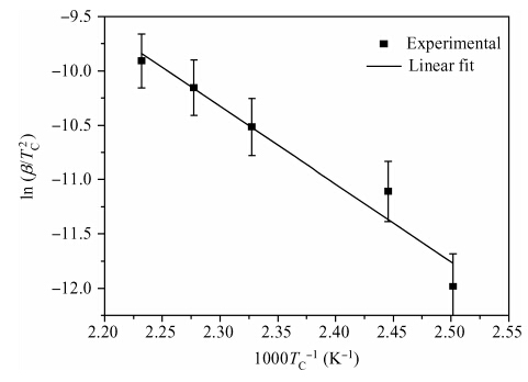
Abstract: The crystallization kinetics of Sn40Se60 thin films has been successfully investigated using sheet resistance versus temperature measurements. Thermal evaporation was used to deposit the films on ordinary glass substrates. The crystallization temperature for Sn40Se60 thin film was found to be 156.6 ± 0.3 ℃. In the as-deposited state, the sheet resistance was found to be 195 MΩ, this value declined to 1560 Ω/口 upon annealing. The value of activation energy obtained from the Kissinger plot was 0.62 ± 0.07 eV. From the results obtained, Sn40Se60 is a promising alloy for PCM application because of its high electrical contrast, high crystallization temperature, and relatively high activation energy.
Keywords: crystallization temperature, activation energy, electrical contrast, phase change memory
| [1] | |
| [2] | |
| [3] | |
| [4] | |
| [5] | |
| [6] | |
| [7] | |
| [8] | |
| [9] | |
| [10] | |
| [11] | |
| [12] | |
| [13] | |
| [14] | |
| [15] | |
| [16] | |
| [17] | |
| [18] | |
| [19] | |
| [20] | |
| [21] | |
| [22] | |
| [23] | |
| [24] | |
| [25] | |
| [26] |
| [1] | |
| [2] | |
| [3] | |
| [4] | |
| [5] | |
| [6] | |
| [7] | |
| [8] | |
| [9] | |
| [10] | |
| [11] | |
| [12] | |
| [13] | |
| [14] | |
| [15] | |
| [16] | |
| [17] | |
| [18] | |
| [19] | |
| [20] | |
| [21] | |
| [22] | |
| [23] | |
| [24] | |
| [25] | |
| [26] |


Article views: 2893 Times PDF downloads: 21 Times Cited by: 0 Times
Received: 19 December 2014 Revised: Online: Published: 01 June 2015
| Citation: |
Joshua M. Kundu, Patrick M. Karimi, Walter K. Njoroge. Crystallization kinetics of Sn40Se60 thin films for phase change memory applications[J]. Journal of Semiconductors, 2015, 36(6): 063002. doi: 10.1088/1674-4926/36/6/063002
****
J. M. Kundu, P. M. Karimi, W. K. Njoroge. Crystallization kinetics of Sn40Se60 thin films for phase change memory applications[J]. J. Semicond., 2015, 36(6): 063002. doi: 10.1088/1674-4926/36/6/063002.

|
| [1] | |
| [2] | |
| [3] | |
| [4] | |
| [5] | |
| [6] | |
| [7] | |
| [8] | |
| [9] | |
| [10] | |
| [11] | |
| [12] | |
| [13] | |
| [14] | |
| [15] | |
| [16] | |
| [17] | |
| [18] | |
| [19] | |
| [20] | |
| [21] | |
| [22] | |
| [23] | |
| [24] | |
| [25] | |
| [26] |

 WeChat ID
Journal of Semiconductors © 2017 All Rights Reserved 京ICP备05085259号-2

 DownLoad:

