


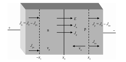
Fig. 1.
Depletion layer of a p-n junction hetero-structure diode reverse-biased to breakdown.
SEMICONDUCTOR DEVICES
Moumita Mukherjee1, P. R. Tripathy2 and S. P. Pati3
Corresponding author: Moumita Mukherjee, Email: mukherjee_phys@yahoo.in;pravashrt76@yahoo.co.in
Abstract: A full-scale, self-consistent, non-linear, large-signal model of double-drift hetero-structure IMPATT diode with general doping profile is derived. This newly developed model, for the first time, has been used to analyze the large-signal characteristics of hexagonal SiC-based double-drift IMPATT diode. Considering the fabrication feasibility, the authors have studied the large-signal characteristics of Si/SiC-based hetero-structure devices. Under small-voltage modulation (~ 2%, i.e. small-signal conditions) results are in good agreement with calculations done using a linearised small-signal model. The large-signal values of the diode's negative conductance (5 × 10⁶S/m2), susceptance (10.4 × 10⁷ S/m2}), average breakdown voltage (207.6 V), and power generating efficiency (15%, RF power: 25.0 W at 94 GHz) are obtained as a function of oscillation amplitude (50% of DC breakdown voltage) for a fixed average current density. The large-signal calculations exhibit power and efficiency saturation for large-signal (> 50%) voltage modulation and thereafter decrease gradually with further increasing voltage-modulation. This generalized large-signal formulation is applicable for all types of IMPATT structures with distributed and narrow avalanche zones. The simulator is made more realistic by incorporating the space-charge effects, realistic field and temperature dependent material parameters in Si and SiC. The electric field snap-shots and the large-signal impedance and admittance of the diode with current excitation are expressed in closed loop form. This study will act as a guide for researchers to fabricate a high-power Si/SiC-based IMPATT for possible application in high-power MM-wave communication systems.
Keywords: Si/SiC hetero-structure double drift diode, full-scale large-signal modelling, high-power, parasitic effects, noise-analysis
| [1] | |
| [2] | |
| [3] | |
| [4] | |
| [5] | |
| [6] | |
| [7] | |
| [8] | |
| [9] | |
| [10] | |
| [11] | |
| [12] | |
| [13] | |
| [14] | |
| [15] |
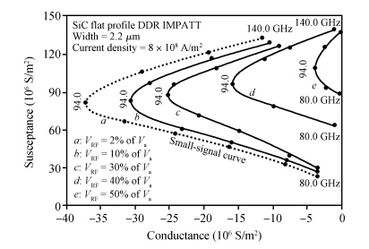
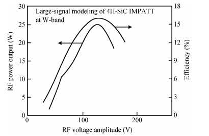
Table 1. Optimised design parameters of Si/SiC DD hetero-structure IMPATTs for large-signal analysis.
 DownLoad: CSV
Table 2. Values of series resistance ($R_{\rm S,total})$ of Si/SiC DD hetero-structure IMPATT [bias current density $=$ 8.0 $\times$ 10$^{8}$ A/m$^{2}$ and frequency $=$ 94 GHz].
DownLoad: CSV
| [1] | |
| [2] | |
| [3] | |
| [4] | |
| [5] | |
| [6] | |
| [7] | |
| [8] | |
| [9] | |
| [10] | |
| [11] | |
| [12] | |
| [13] | |
| [14] | |
| [15] |


Article views: 3209 Times PDF downloads: 21 Times Cited by: 0 Times
Received: 14 November 2014 Revised: Online: Published: 01 June 2015
| Citation: |
Moumita Mukherjee, P. R. Tripathy, S. P. Pati. Si/SiC-based DD hetero-structure IMPATTs as MM-wave power-source: a generalized large-signal analysis[J]. Journal of Semiconductors, 2015, 36(6): 064005. doi: 10.1088/1674-4926/36/6/064005
****
M Mukherjee, P. R. Tripathy, S. P. Pati. Si/SiC-based DD hetero-structure IMPATTs as MM-wave power-source: a generalized large-signal analysis[J]. J. Semicond., 2015, 36(6): 064005. doi: 10.1088/1674-4926/36/6/064005.

|
| [1] | |
| [2] | |
| [3] | |
| [4] | |
| [5] | |
| [6] | |
| [7] | |
| [8] | |
| [9] | |
| [10] | |
| [11] | |
| [12] | |
| [13] | |
| [14] | |
| [15] |

 WeChat ID
Journal of Semiconductors © 2017 All Rights Reserved 京ICP备05085259号-2


