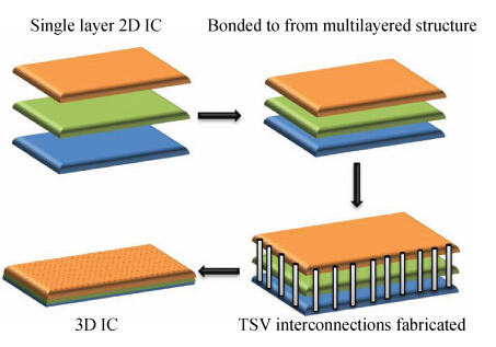
Fig. 1.
A schematic of 3D integration.
SEMICONDUCTOR INTEGRATED CIRCUITS
Tanu Goyal1, Manoj Kumar Majumder2 and Brajesh Kumar Kaushik2
Corresponding author: Tanu Goyal, Email: tanugoy007@gmail.com; Manoj Kumar Majumder, Email: manojbesu@gmail.com; Brajesh Kumar Kaushik, Email: bkk23fec@iitr.ac.in
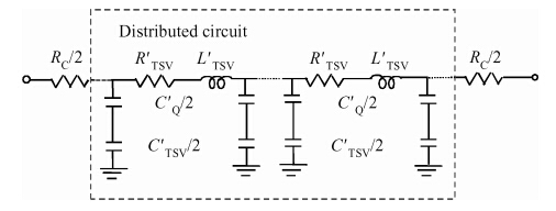
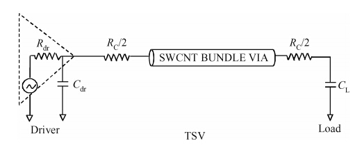
Abstract: Through-silicon vias (TSVs) have provided an attractive solution for three-dimensional (3D) integrated devices and circuit technologies with reduced parasitic losses and power dissipation, higher input-output (I/O) density and improved system performance. This paper investigates the propagation delay and average power dissipation of single-walled carbon nanotube bundled TSVs having different via radius and height. Depending on the physical configuration, a comprehensive and accurate analytical model of CNT bundled TSV is employed to represent the via (vertical interconnect access) line of a driver-TSV-load (DTL) system. The via radius and height are used to estimate the bundle aspect ratio (AR) and the cross-sectional area. For a fixed via height, the delay and the power dissipation are reduced up to 96.2% using a SWCNT bundled TSV with AR = 300 : 1 in comparison to AR = 6 : 1.
Keywords: carbon nanotube, through-silicon vias, equivalent RLC circuit model, propagation delay, power-delay product, area-delay product
| [1] | |
| [2] | |
| [3] | |
| [4] | |
| [5] | |
| [6] | |
| [7] | |
| [8] | |
| [9] | |
| [10] | |
| [11] | |
| [12] | |
| [13] | |
| [14] | |
| [15] | |
| [16] | |
| [17] | |
| [18] | |
| [19] | |
| [20] | |
| [21] | |
| [22] | |
| [23] | |
| [24] | |
| [25] |
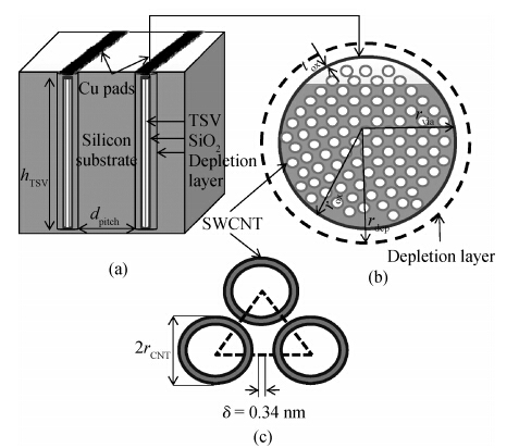
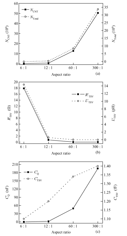
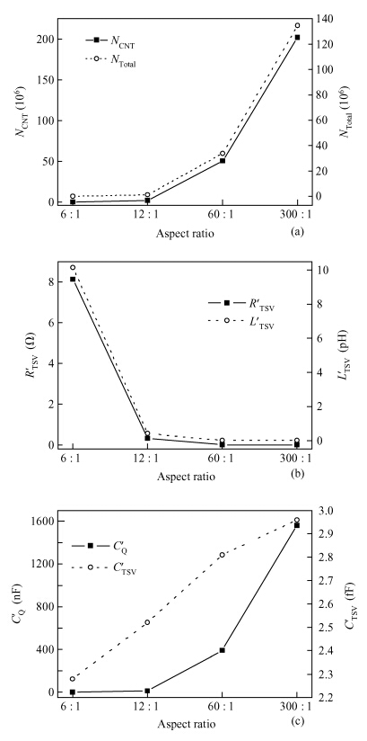
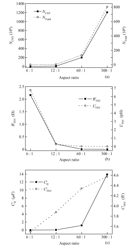
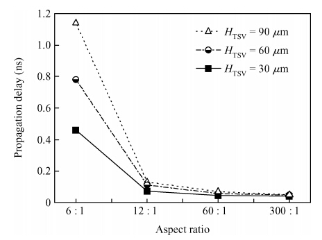
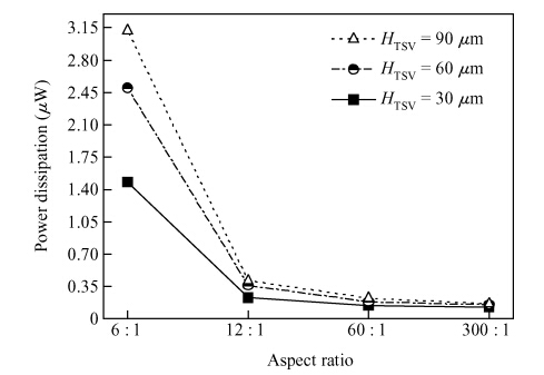
Table 2. Percentage reduction in delay and power dissipation of SWCNT bundled TSVs for AR D 300 : 1
 DownLoad: CSV
Table 3. Percentage reduction in power delay product of SWCNT bundled TSVs for AR $=$ 300 : 1.
DownLoad: CSV
Table 4. Percentage reduction in area delay product of SWCNT bundled TSVs for AR $=$ 300 : 1.
DownLoad: CSV
Table 5. Variation of cross-sectional area of bundled SWCNT TSVs with different aspect ratio.
DownLoad: CSV
| [1] | |
| [2] | |
| [3] | |
| [4] | |
| [5] | |
| [6] | |
| [7] | |
| [8] | |
| [9] | |
| [10] | |
| [11] | |
| [12] | |
| [13] | |
| [14] | |
| [15] | |
| [16] | |
| [17] | |
| [18] | |
| [19] | |
| [20] | |
| [21] | |
| [22] | |
| [23] | |
| [24] | |
| [25] |


Article views: 3302 Times PDF downloads: 19 Times Cited by: 0 Times
Received: 20 October 2014 Revised: Online: Published: 01 June 2015
| Citation: |
Tanu Goyal, Manoj Kumar Majumder, Brajesh Kumar Kaushik. Propagation delay and power dissipation for different aspect ratio of single-walled carbon nanotube bundled TSV[J]. Journal of Semiconductors, 2015, 36(6): 065001. doi: 10.1088/1674-4926/36/6/065001
****
T Goyal, M K Majumder, B K Kaushik. Propagation delay and power dissipation for different aspect ratio of single-walled carbon nanotube bundled TSV[J]. J. Semicond., 2015, 36(6): 065001. doi: 10.1088/1674-4926/36/6/065001.

|
| [1] | |
| [2] | |
| [3] | |
| [4] | |
| [5] | |
| [6] | |
| [7] | |
| [8] | |
| [9] | |
| [10] | |
| [11] | |
| [12] | |
| [13] | |
| [14] | |
| [15] | |
| [16] | |
| [17] | |
| [18] | |
| [19] | |
| [20] | |
| [21] | |
| [22] | |
| [23] | |
| [24] | |
| [25] |

 WeChat ID
Journal of Semiconductors © 2017 All Rights Reserved 京ICP备05085259号-2