


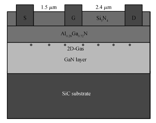
Fig. 1.
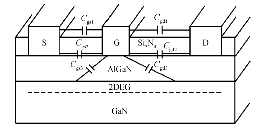
Cross section of device structure.
SEMICONDUCTOR DEVICES
Lei Shi, Shiwei Feng, Kun Liu and Yamin Zhang
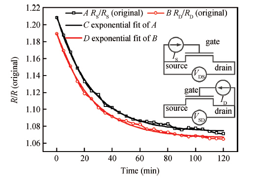
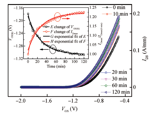
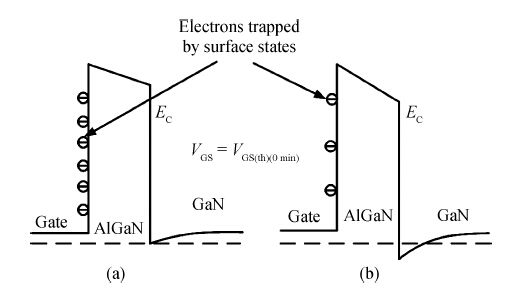
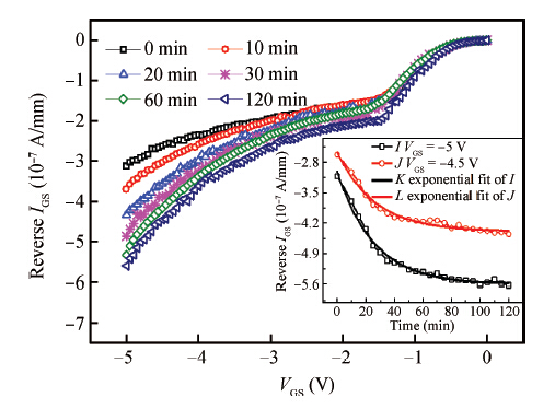
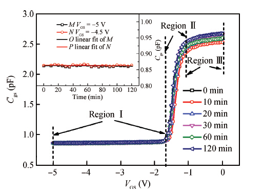
Abstract: The phenomenon of self-changing on the device parameters and characteristics after a step voltage stress was applied to the gate is studied in AlGaN/GaN high electron mobility transistors. The device was measured every 5 min after the stress was removed. The large-signal parasitic source (drain) resistance, transfer characteristics, threshold voltage, drain-source current, gate-source (drain) reverse current-voltage characteristics changed spontaneously after the removal of the stress. The time constant of the self-changing was about 25-27 min. The gate-source (drain) capacitance-voltage characteristics were constant during this process. Electrons were trapped by the surface states and traps in the AlGaN barrier layer when the device was under stress. The traps in the AlGaN barrier layer then released electrons in less than 10 s. The surface states released electrons continuously during the entire measurement stage, leading to the self-changing of mearsurement result.
Keywords: AlGaN/GaN HEMTs, surface states, self-changing, stress
| [1] | |
| [2] | |
| [3] | |
| [4] | |
| [5] | |
| [6] | |
| [7] | |
| [8] | |
| [9] | |
| [10] | |
| [11] | |
| [12] | |
| [13] | |
| [14] | |
| [15] | |
| [16] |
| [1] | |
| [2] | |
| [3] | |
| [4] | |
| [5] | |
| [6] | |
| [7] | |
| [8] | |
| [9] | |
| [10] | |
| [11] | |
| [12] | |
| [13] | |
| [14] | |
| [15] | |
| [16] |


Article views: 2751 Times PDF downloads: 21 Times Cited by: 0 Times
Received: 05 September 2014 Revised: Online: Published: 01 July 2015
| Citation: |
Lei Shi, Shiwei Feng, Kun Liu, Yamin Zhang. Mechanism of the self-changing parameters and characteristics in AlGaN/GaN high-electron mobility transistors after a step voltage stress[J]. Journal of Semiconductors, 2015, 36(7): 074005. doi: 10.1088/1674-4926/36/7/074005
****
L Shi, S W Feng, K Liu, Y M Zhang. Mechanism of the self-changing parameters and characteristics in AlGaN/GaN high-electron mobility transistors after a step voltage stress[J]. J. Semicond., 2015, 36(7): 074005. doi: 10.1088/1674-4926/36/7/074005.

|
| [1] | |
| [2] | |
| [3] | |
| [4] | |
| [5] | |
| [6] | |
| [7] | |
| [8] | |
| [9] | |
| [10] | |
| [11] | |
| [12] | |
| [13] | |
| [14] | |
| [15] | |
| [16] |

 WeChat ID
Journal of Semiconductors © 2017 All Rights Reserved 京ICP备05085259号-2

 DownLoad:

