Fig. 1.
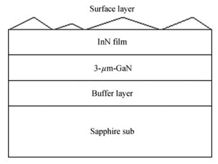
Optical models used in data analysis.
SEMICONDUCTOR PHYSICS
Chunya Ye, Wei Lin, Jin Zhou, Shuping Li, Li Chen, Heng Li, Xiaoxuan Wu, Songqing Liu and Junyong Kang
Corresponding author: Li Shuping, Email: lsp@xmu.edu.cn
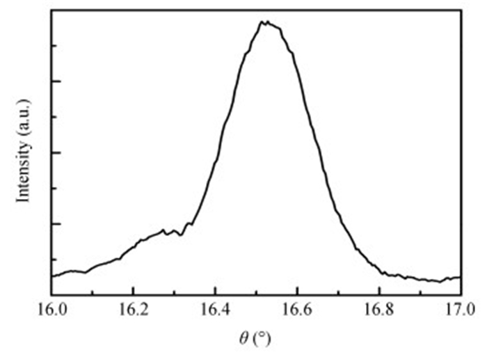
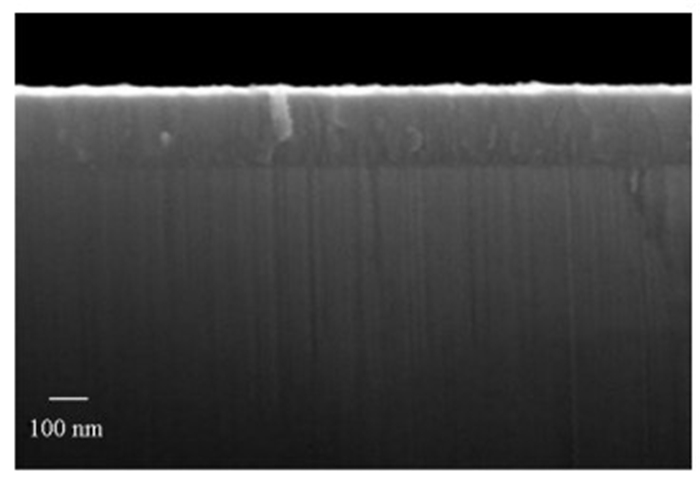
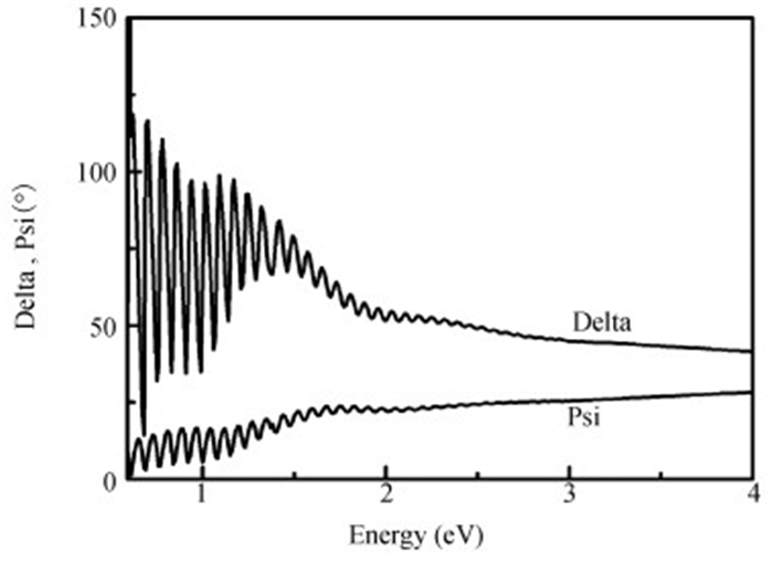
Abstract: With recently developed InN epitaxy via a controlling In bilayer, spectroscopic ellipsometry (SE) measurements had been carried out on the grown InN and the measured ellipsometric spectra were fitted with the Delta Psi2 software by using a suitable model and the dispersion rule. The thickness was measured by a scanning electron microscope (SEM). Insight into the film quality of InN and the lattice constant were gained by X-ray diffraction (XRD). By fitting the SE, the thickness of the InN film is consistent with that obtained by SEM cross-sectional thickness measurement. The optical bandgap of InN was put forward to be 1.05 eV, which conforms to the experimental results measured by the absorption spectrum and cathodoluminescence (CL). The refractive index and the extinction coefficient of interest were represented for InN, which is useful to design optoelectronic devices.
Keywords: InN, spectroscopic ellipsometry, refractive index, extinction coefficient
| [1] |
Nakamura S, Fasol G. The blue laser diode—GaN-based light emitting diode and lasers. Heidelberg: Springer-Verlag, 1997
|
| [2] |
Lorenz K, Franco N, Alves E, et al. Relaxation of compressively strained AlInN on GaN. J Cryst Growth, 2008, 310(18): 4058 doi: 10.1016/j.jcrysgro.2008.07.006
|
| [3] |
Liu Na, Yi Xiaoyan, Liang Meng, et al. Effects of the p-AlInGaN/GaN superlattices' structure on the performance of blue LEDs. Journal of Semiconductors, 2014, 35(2): 024010 doi: 10.1088/1674-4926/35/2/024010
|
| [4] |
Jing Liang, Xiao Hongling, Wang Xiaoliang, et al. Enhanced performance of InGaN/GaN multiple quantum well solar cells with patterned sapphire substrate. Journal of Semiconductors, 2013, 34(12): 124004 doi: 10.1088/1674-4926/34/12/124004
|
| [5] |
Gan C K, Srolovitz D J. First-principles study of wurtzite InN (0001) and (0001) surfaces. Phys Rev B, 2006, 74(11): 115319 doi: 10.1103/PhysRevB.74.115319
|
| [6] |
Inushima T, Mamutin V V, Vekshin V A, et al. Physical properties of InN with the band gap energy of 1.1 eV. J Cryst Growth, 2001, 227/228(01): 481 http://cn.bing.com/academic/profile?id=2071345739&encoded=0&v=paper_preview&mkt=zh-cn
|
| [7] |
Davydov V Y, Klochikhin A A, Seisyan R P, et al. Absorption and emission of hexagonal InN. evidence of narrow fundamental band gap. Physica Status Solidi, 2002, 229(3): r1 doi: 10.1002/(ISSN)1521-3951
|
| [8] |
Wu J, Walukiewicz W, Yu K M, et al. Unusual properties of the fundamental band gap of InN. Appl Phys Lett, 2002, 80(21): 3967 doi: 10.1063/1.1482786
|
| [9] |
Wang H, Jiang D S, Zhu J J, et al. The influence of growth temperature and input V/Ⅲ ratio on the initial nucleation and material properties of InN on GaN by MOCVD. Semicond Sci Technol, 2009, 24(5): 177 http://cn.bing.com/academic/profile?id=1996691121&encoded=0&v=paper_preview&mkt=zh-cn
|
| [10] |
Laskar M R, Ganguli T, Kadir A, et al. Influence of buffer layers on the microstructure of MOVPE grown a-plane InN. J Cryst Growth, 2011, 315(1): 233 doi: 10.1016/j.jcrysgro.2010.08.019
|
| [11] |
Djurišić A B, Li E H. Modeling the optical constants of hexagonal GaN, InN, and AlN. J Appl Phys, 1999, 85(5): 2848 doi: 10.1063/1.369604
|
| [12] |
Yu Tongjun, Kang Xiangning, Qin Zhixin, et al. Strain effect on photoluminescence from InGaN/GaN and InGaN/AlGaN MQWs. Journal of Semiconductors, 2006, 27(13): 20 http://www.jos.ac.cn/bdtxbcn/ch/reader/view_abstract.aspx?flag=1&file_no=200613005&journal_id=bdtxbcn
|
| [13] |
Tao Tao, Zhang Zhao, Liu Lian, et al. Surface morphology and composition studies in InGaN/GaN film grown by MOCVD. Journal of Semiconductors, 2011, 32(8): 083002 doi: 10.1088/1674-4926/32/8/083002
|
| [14] |
Zhou Jin, Huang Qiangcan, Li Jinchai, et al. The InN epitaxy via controlling In bilayer. Nanoscale Research Letters, 2014, 9: 5 doi: 10.1186/1556-276X-9-5
|
| [15] |
Lee J H, Lee B, Kang J H, et al. Optical characterization of nanoporous GaN by spectroscopic ellipsometry. Thin Solid Films, 2012, 525(12): 84 http://cn.bing.com/academic/profile?id=2065377105&encoded=0&v=paper_preview&mkt=zh-cn
|
| [16] |
Azzam R M A, Bashara N M, Burns D T, et al. Ellipsometry and polarized light. North Holland, 1987
|
| [17] |
Barshilia H C, Selvakumar N, Rajam K S, et al. TiAlN/TiAlON/Si3N4 tandem absorber for high temperature solar selective applications. Appl Phys Lett, 2006, 89(19): 191909 doi: 10.1063/1.2387897
|
| [18] |
Bhattacharyya D, Biswas A, Sahoo N K. Investigation on dispersion of optical constants of Gd2O3 films by phase modulated spectroscopic ellipsometry. J Appl Phys, 2004, 233(1-4): 155 http://cn.bing.com/academic/profile?id=2077091620&encoded=0&v=paper_preview&mkt=zh-cn
|
| [19] |
Drévillon B. Phase modulated ellipsometry from the ultraviolet to the infrared: in situ application to the growth of semiconductors. Progress in Crystal Growth & Characterization of Materials, 1993, 27(1): 1 http://cn.bing.com/academic/profile?id=1982488675&encoded=0&v=paper_preview&mkt=zh-cn
|
| [20] |
Xiong Y M, Snyder P G. Variable angle spectroscopic ellipsometric characterization of surface damage in chemical-mechanical polished GaAs. Thin Solid Films, 1992, 220(1/2): 303 http://cn.bing.com/academic/profile?id=1974362142&encoded=0&v=paper_preview&mkt=zh-cn
|
| [21] |
Biswas A, Yadav B S, Bhattacharyya D, et al. Spectroscopic ellipsometry studies of reactively sputtered nitrogen-rich GaAsN films. J Non-Cryst Solids, 2011, 357(18): 3293 doi: 10.1016/j.jnoncrysol.2011.06.007
|
| [22] |
Jiang W, Lin W, Li S P, et al. Optical anisotropy of AlN epilayer on sapphire substrate investigated by variable-angle spectroscopic ellipsometry. Optical Materials, 2010, 32: 891 doi: 10.1016/j.optmat.2010.01.015
|
| [23] |
Kisielowski C. Semiconductor and Semimetals. 1998, Chap 7
|
| [24] |
Zhao Y, Wang H, Wu G G, et al. Effect of nitridation on structure, electrical and optical properties of InN epilayers grown on sapphire by PAMBE. Vacuum, 2015, 111: 15 doi: 10.1016/j.vacuum.2014.09.014
|
| [25] |
Zhao Y, Wang H, Yang H, et al. Growth temperature induced physical property variation of InN films grown on nitrided sapphire substrate by PAMBE. Vacuum, 2015, 112: 55 doi: 10.1016/j.vacuum.2014.11.016
|
| [26] |
Tanguy C, Lefebvre P, Mathieu H, et al. Analytical model for the refractive index in quantum wells derived from the complex dielectric constant of Wannier excitons in noninteger dimensions. J Appl Phys, 1997, 82: 798 doi: 10.1063/1.365580
|
| [27] |
Tanguy C. Optical dispersion by Wannier excitons. Phys Rev Lett, 1995, 75: 4090 doi: 10.1103/PhysRevLett.75.4090
|
| [28] |
Yu Yangjing, Zhang Bin, Li Hongyi, et al. Study on the GaN film by spectroscopic ellipsometry. Semiconductor Technology, 2011, 36(11): 821 http://cn.bing.com/academic/profile?id=1967417357&encoded=0&v=paper_preview&mkt=zh-cn
|
| [29] |
Yan Q, Rinke P, Janotti A, et al. Effects of strain on the band structure of group-Ⅲ nitrides. Phys Rev B, 2014, 90(12): 125118 doi: 10.1103/PhysRevB.90.125118
|
| [30] |
Tanaka K, Kondo T. Bandgap and exciton binding energies in lead-iodide-based natural quantum-well crystals. Science and Technology of Advanced Materials, 2013, 4: 599 http://cn.bing.com/academic/profile?id=1965751299&encoded=0&v=paper_preview&mkt=zh-cn
|
| [31] |
Wang Dongpo, Li Weitu. Determining of infrared transition of InN film grown on c-plane sapphire by photoreflectance. Applied Mechanics and Materials, 2012, 110: 985 http://cn.bing.com/academic/profile?id=1966995937&encoded=0&v=paper_preview&mkt=zh-cn
|
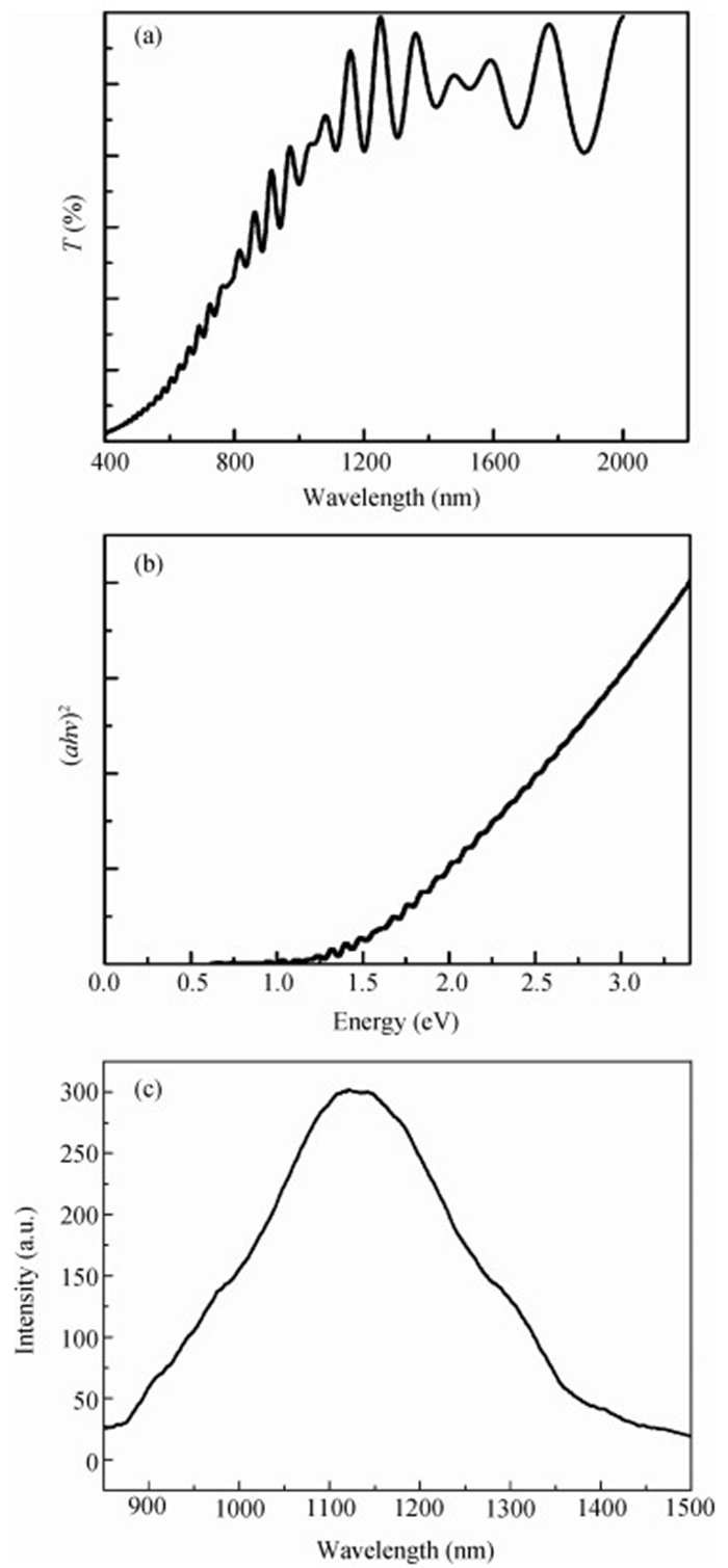
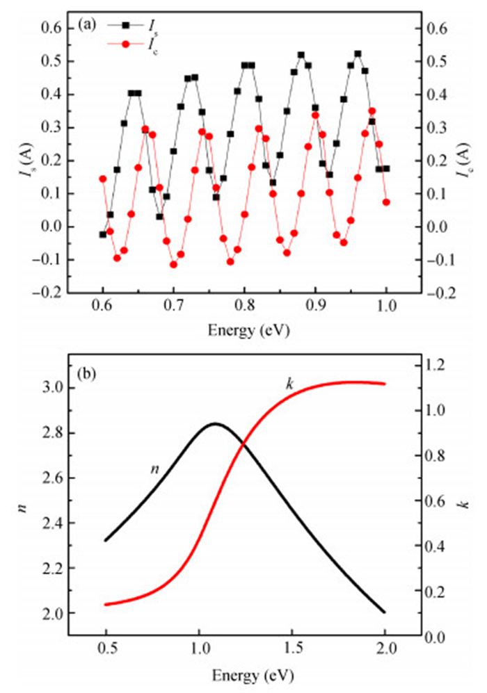
Table 1. The lattice constant and thermal expansion coefficient of GaN and InN.

|
| [1] |
Nakamura S, Fasol G. The blue laser diode—GaN-based light emitting diode and lasers. Heidelberg: Springer-Verlag, 1997
|
| [2] |
Lorenz K, Franco N, Alves E, et al. Relaxation of compressively strained AlInN on GaN. J Cryst Growth, 2008, 310(18): 4058 doi: 10.1016/j.jcrysgro.2008.07.006
|
| [3] |
Liu Na, Yi Xiaoyan, Liang Meng, et al. Effects of the p-AlInGaN/GaN superlattices' structure on the performance of blue LEDs. Journal of Semiconductors, 2014, 35(2): 024010 doi: 10.1088/1674-4926/35/2/024010
|
| [4] |
Jing Liang, Xiao Hongling, Wang Xiaoliang, et al. Enhanced performance of InGaN/GaN multiple quantum well solar cells with patterned sapphire substrate. Journal of Semiconductors, 2013, 34(12): 124004 doi: 10.1088/1674-4926/34/12/124004
|
| [5] |
Gan C K, Srolovitz D J. First-principles study of wurtzite InN (0001) and (0001) surfaces. Phys Rev B, 2006, 74(11): 115319 doi: 10.1103/PhysRevB.74.115319
|
| [6] |
Inushima T, Mamutin V V, Vekshin V A, et al. Physical properties of InN with the band gap energy of 1.1 eV. J Cryst Growth, 2001, 227/228(01): 481 http://cn.bing.com/academic/profile?id=2071345739&encoded=0&v=paper_preview&mkt=zh-cn
|
| [7] |
Davydov V Y, Klochikhin A A, Seisyan R P, et al. Absorption and emission of hexagonal InN. evidence of narrow fundamental band gap. Physica Status Solidi, 2002, 229(3): r1 doi: 10.1002/(ISSN)1521-3951
|
| [8] |
Wu J, Walukiewicz W, Yu K M, et al. Unusual properties of the fundamental band gap of InN. Appl Phys Lett, 2002, 80(21): 3967 doi: 10.1063/1.1482786
|
| [9] |
Wang H, Jiang D S, Zhu J J, et al. The influence of growth temperature and input V/Ⅲ ratio on the initial nucleation and material properties of InN on GaN by MOCVD. Semicond Sci Technol, 2009, 24(5): 177 http://cn.bing.com/academic/profile?id=1996691121&encoded=0&v=paper_preview&mkt=zh-cn
|
| [10] |
Laskar M R, Ganguli T, Kadir A, et al. Influence of buffer layers on the microstructure of MOVPE grown a-plane InN. J Cryst Growth, 2011, 315(1): 233 doi: 10.1016/j.jcrysgro.2010.08.019
|
| [11] |
Djurišić A B, Li E H. Modeling the optical constants of hexagonal GaN, InN, and AlN. J Appl Phys, 1999, 85(5): 2848 doi: 10.1063/1.369604
|
| [12] |
Yu Tongjun, Kang Xiangning, Qin Zhixin, et al. Strain effect on photoluminescence from InGaN/GaN and InGaN/AlGaN MQWs. Journal of Semiconductors, 2006, 27(13): 20 http://www.jos.ac.cn/bdtxbcn/ch/reader/view_abstract.aspx?flag=1&file_no=200613005&journal_id=bdtxbcn
|
| [13] |
Tao Tao, Zhang Zhao, Liu Lian, et al. Surface morphology and composition studies in InGaN/GaN film grown by MOCVD. Journal of Semiconductors, 2011, 32(8): 083002 doi: 10.1088/1674-4926/32/8/083002
|
| [14] |
Zhou Jin, Huang Qiangcan, Li Jinchai, et al. The InN epitaxy via controlling In bilayer. Nanoscale Research Letters, 2014, 9: 5 doi: 10.1186/1556-276X-9-5
|
| [15] |
Lee J H, Lee B, Kang J H, et al. Optical characterization of nanoporous GaN by spectroscopic ellipsometry. Thin Solid Films, 2012, 525(12): 84 http://cn.bing.com/academic/profile?id=2065377105&encoded=0&v=paper_preview&mkt=zh-cn
|
| [16] |
Azzam R M A, Bashara N M, Burns D T, et al. Ellipsometry and polarized light. North Holland, 1987
|
| [17] |
Barshilia H C, Selvakumar N, Rajam K S, et al. TiAlN/TiAlON/Si3N4 tandem absorber for high temperature solar selective applications. Appl Phys Lett, 2006, 89(19): 191909 doi: 10.1063/1.2387897
|
| [18] |
Bhattacharyya D, Biswas A, Sahoo N K. Investigation on dispersion of optical constants of Gd2O3 films by phase modulated spectroscopic ellipsometry. J Appl Phys, 2004, 233(1-4): 155 http://cn.bing.com/academic/profile?id=2077091620&encoded=0&v=paper_preview&mkt=zh-cn
|
| [19] |
Drévillon B. Phase modulated ellipsometry from the ultraviolet to the infrared: in situ application to the growth of semiconductors. Progress in Crystal Growth & Characterization of Materials, 1993, 27(1): 1 http://cn.bing.com/academic/profile?id=1982488675&encoded=0&v=paper_preview&mkt=zh-cn
|
| [20] |
Xiong Y M, Snyder P G. Variable angle spectroscopic ellipsometric characterization of surface damage in chemical-mechanical polished GaAs. Thin Solid Films, 1992, 220(1/2): 303 http://cn.bing.com/academic/profile?id=1974362142&encoded=0&v=paper_preview&mkt=zh-cn
|
| [21] |
Biswas A, Yadav B S, Bhattacharyya D, et al. Spectroscopic ellipsometry studies of reactively sputtered nitrogen-rich GaAsN films. J Non-Cryst Solids, 2011, 357(18): 3293 doi: 10.1016/j.jnoncrysol.2011.06.007
|
| [22] |
Jiang W, Lin W, Li S P, et al. Optical anisotropy of AlN epilayer on sapphire substrate investigated by variable-angle spectroscopic ellipsometry. Optical Materials, 2010, 32: 891 doi: 10.1016/j.optmat.2010.01.015
|
| [23] |
Kisielowski C. Semiconductor and Semimetals. 1998, Chap 7
|
| [24] |
Zhao Y, Wang H, Wu G G, et al. Effect of nitridation on structure, electrical and optical properties of InN epilayers grown on sapphire by PAMBE. Vacuum, 2015, 111: 15 doi: 10.1016/j.vacuum.2014.09.014
|
| [25] |
Zhao Y, Wang H, Yang H, et al. Growth temperature induced physical property variation of InN films grown on nitrided sapphire substrate by PAMBE. Vacuum, 2015, 112: 55 doi: 10.1016/j.vacuum.2014.11.016
|
| [26] |
Tanguy C, Lefebvre P, Mathieu H, et al. Analytical model for the refractive index in quantum wells derived from the complex dielectric constant of Wannier excitons in noninteger dimensions. J Appl Phys, 1997, 82: 798 doi: 10.1063/1.365580
|
| [27] |
Tanguy C. Optical dispersion by Wannier excitons. Phys Rev Lett, 1995, 75: 4090 doi: 10.1103/PhysRevLett.75.4090
|
| [28] |
Yu Yangjing, Zhang Bin, Li Hongyi, et al. Study on the GaN film by spectroscopic ellipsometry. Semiconductor Technology, 2011, 36(11): 821 http://cn.bing.com/academic/profile?id=1967417357&encoded=0&v=paper_preview&mkt=zh-cn
|
| [29] |
Yan Q, Rinke P, Janotti A, et al. Effects of strain on the band structure of group-Ⅲ nitrides. Phys Rev B, 2014, 90(12): 125118 doi: 10.1103/PhysRevB.90.125118
|
| [30] |
Tanaka K, Kondo T. Bandgap and exciton binding energies in lead-iodide-based natural quantum-well crystals. Science and Technology of Advanced Materials, 2013, 4: 599 http://cn.bing.com/academic/profile?id=1965751299&encoded=0&v=paper_preview&mkt=zh-cn
|
| [31] |
Wang Dongpo, Li Weitu. Determining of infrared transition of InN film grown on c-plane sapphire by photoreflectance. Applied Mechanics and Materials, 2012, 110: 985 http://cn.bing.com/academic/profile?id=1966995937&encoded=0&v=paper_preview&mkt=zh-cn
|


Article views: 4017 Times PDF downloads: 50 Times Cited by: 0 Times
Received: 22 February 2016 Revised: 27 April 2016 Online: Published: 01 October 2016
| Citation: |
Chunya Ye, Wei Lin, Jin Zhou, Shuping Li, Li Chen, Heng Li, Xiaoxuan Wu, Songqing Liu, Junyong Kang. Optical properties of InN studied by spectroscopic ellipsometry[J]. Journal of Semiconductors, 2016, 37(10): 102002. doi: 10.1088/1674-4926/37/10/102002
****
C Y Ye, W Lin, J Zhou, S P Li, L Chen, H Li, X X Wu, S Q Liu, J Y Kang. Optical properties of InN studied by spectroscopic ellipsometry[J]. J. Semicond., 2016, 37(10): 102002. doi: 10.1088/1674-4926/37/10/102002.

|
| [1] |
Nakamura S, Fasol G. The blue laser diode—GaN-based light emitting diode and lasers. Heidelberg: Springer-Verlag, 1997
|
| [2] |
Lorenz K, Franco N, Alves E, et al. Relaxation of compressively strained AlInN on GaN. J Cryst Growth, 2008, 310(18): 4058 doi: 10.1016/j.jcrysgro.2008.07.006
|
| [3] |
Liu Na, Yi Xiaoyan, Liang Meng, et al. Effects of the p-AlInGaN/GaN superlattices' structure on the performance of blue LEDs. Journal of Semiconductors, 2014, 35(2): 024010 doi: 10.1088/1674-4926/35/2/024010
|
| [4] |
Jing Liang, Xiao Hongling, Wang Xiaoliang, et al. Enhanced performance of InGaN/GaN multiple quantum well solar cells with patterned sapphire substrate. Journal of Semiconductors, 2013, 34(12): 124004 doi: 10.1088/1674-4926/34/12/124004
|
| [5] |
Gan C K, Srolovitz D J. First-principles study of wurtzite InN (0001) and (0001) surfaces. Phys Rev B, 2006, 74(11): 115319 doi: 10.1103/PhysRevB.74.115319
|
| [6] |
Inushima T, Mamutin V V, Vekshin V A, et al. Physical properties of InN with the band gap energy of 1.1 eV. J Cryst Growth, 2001, 227/228(01): 481 http://cn.bing.com/academic/profile?id=2071345739&encoded=0&v=paper_preview&mkt=zh-cn
|
| [7] |
Davydov V Y, Klochikhin A A, Seisyan R P, et al. Absorption and emission of hexagonal InN. evidence of narrow fundamental band gap. Physica Status Solidi, 2002, 229(3): r1 doi: 10.1002/(ISSN)1521-3951
|
| [8] |
Wu J, Walukiewicz W, Yu K M, et al. Unusual properties of the fundamental band gap of InN. Appl Phys Lett, 2002, 80(21): 3967 doi: 10.1063/1.1482786
|
| [9] |
Wang H, Jiang D S, Zhu J J, et al. The influence of growth temperature and input V/Ⅲ ratio on the initial nucleation and material properties of InN on GaN by MOCVD. Semicond Sci Technol, 2009, 24(5): 177 http://cn.bing.com/academic/profile?id=1996691121&encoded=0&v=paper_preview&mkt=zh-cn
|
| [10] |
Laskar M R, Ganguli T, Kadir A, et al. Influence of buffer layers on the microstructure of MOVPE grown a-plane InN. J Cryst Growth, 2011, 315(1): 233 doi: 10.1016/j.jcrysgro.2010.08.019
|
| [11] |
Djurišić A B, Li E H. Modeling the optical constants of hexagonal GaN, InN, and AlN. J Appl Phys, 1999, 85(5): 2848 doi: 10.1063/1.369604
|
| [12] |
Yu Tongjun, Kang Xiangning, Qin Zhixin, et al. Strain effect on photoluminescence from InGaN/GaN and InGaN/AlGaN MQWs. Journal of Semiconductors, 2006, 27(13): 20 http://www.jos.ac.cn/bdtxbcn/ch/reader/view_abstract.aspx?flag=1&file_no=200613005&journal_id=bdtxbcn
|
| [13] |
Tao Tao, Zhang Zhao, Liu Lian, et al. Surface morphology and composition studies in InGaN/GaN film grown by MOCVD. Journal of Semiconductors, 2011, 32(8): 083002 doi: 10.1088/1674-4926/32/8/083002
|
| [14] |
Zhou Jin, Huang Qiangcan, Li Jinchai, et al. The InN epitaxy via controlling In bilayer. Nanoscale Research Letters, 2014, 9: 5 doi: 10.1186/1556-276X-9-5
|
| [15] |
Lee J H, Lee B, Kang J H, et al. Optical characterization of nanoporous GaN by spectroscopic ellipsometry. Thin Solid Films, 2012, 525(12): 84 http://cn.bing.com/academic/profile?id=2065377105&encoded=0&v=paper_preview&mkt=zh-cn
|
| [16] |
Azzam R M A, Bashara N M, Burns D T, et al. Ellipsometry and polarized light. North Holland, 1987
|
| [17] |
Barshilia H C, Selvakumar N, Rajam K S, et al. TiAlN/TiAlON/Si3N4 tandem absorber for high temperature solar selective applications. Appl Phys Lett, 2006, 89(19): 191909 doi: 10.1063/1.2387897
|
| [18] |
Bhattacharyya D, Biswas A, Sahoo N K. Investigation on dispersion of optical constants of Gd2O3 films by phase modulated spectroscopic ellipsometry. J Appl Phys, 2004, 233(1-4): 155 http://cn.bing.com/academic/profile?id=2077091620&encoded=0&v=paper_preview&mkt=zh-cn
|
| [19] |
Drévillon B. Phase modulated ellipsometry from the ultraviolet to the infrared: in situ application to the growth of semiconductors. Progress in Crystal Growth & Characterization of Materials, 1993, 27(1): 1 http://cn.bing.com/academic/profile?id=1982488675&encoded=0&v=paper_preview&mkt=zh-cn
|
| [20] |
Xiong Y M, Snyder P G. Variable angle spectroscopic ellipsometric characterization of surface damage in chemical-mechanical polished GaAs. Thin Solid Films, 1992, 220(1/2): 303 http://cn.bing.com/academic/profile?id=1974362142&encoded=0&v=paper_preview&mkt=zh-cn
|
| [21] |
Biswas A, Yadav B S, Bhattacharyya D, et al. Spectroscopic ellipsometry studies of reactively sputtered nitrogen-rich GaAsN films. J Non-Cryst Solids, 2011, 357(18): 3293 doi: 10.1016/j.jnoncrysol.2011.06.007
|
| [22] |
Jiang W, Lin W, Li S P, et al. Optical anisotropy of AlN epilayer on sapphire substrate investigated by variable-angle spectroscopic ellipsometry. Optical Materials, 2010, 32: 891 doi: 10.1016/j.optmat.2010.01.015
|
| [23] |
Kisielowski C. Semiconductor and Semimetals. 1998, Chap 7
|
| [24] |
Zhao Y, Wang H, Wu G G, et al. Effect of nitridation on structure, electrical and optical properties of InN epilayers grown on sapphire by PAMBE. Vacuum, 2015, 111: 15 doi: 10.1016/j.vacuum.2014.09.014
|
| [25] |
Zhao Y, Wang H, Yang H, et al. Growth temperature induced physical property variation of InN films grown on nitrided sapphire substrate by PAMBE. Vacuum, 2015, 112: 55 doi: 10.1016/j.vacuum.2014.11.016
|
| [26] |
Tanguy C, Lefebvre P, Mathieu H, et al. Analytical model for the refractive index in quantum wells derived from the complex dielectric constant of Wannier excitons in noninteger dimensions. J Appl Phys, 1997, 82: 798 doi: 10.1063/1.365580
|
| [27] |
Tanguy C. Optical dispersion by Wannier excitons. Phys Rev Lett, 1995, 75: 4090 doi: 10.1103/PhysRevLett.75.4090
|
| [28] |
Yu Yangjing, Zhang Bin, Li Hongyi, et al. Study on the GaN film by spectroscopic ellipsometry. Semiconductor Technology, 2011, 36(11): 821 http://cn.bing.com/academic/profile?id=1967417357&encoded=0&v=paper_preview&mkt=zh-cn
|
| [29] |
Yan Q, Rinke P, Janotti A, et al. Effects of strain on the band structure of group-Ⅲ nitrides. Phys Rev B, 2014, 90(12): 125118 doi: 10.1103/PhysRevB.90.125118
|
| [30] |
Tanaka K, Kondo T. Bandgap and exciton binding energies in lead-iodide-based natural quantum-well crystals. Science and Technology of Advanced Materials, 2013, 4: 599 http://cn.bing.com/academic/profile?id=1965751299&encoded=0&v=paper_preview&mkt=zh-cn
|
| [31] |
Wang Dongpo, Li Weitu. Determining of infrared transition of InN film grown on c-plane sapphire by photoreflectance. Applied Mechanics and Materials, 2012, 110: 985 http://cn.bing.com/academic/profile?id=1966995937&encoded=0&v=paper_preview&mkt=zh-cn
|

 WeChat ID
Journal of Semiconductors © 2017 All Rights Reserved 京ICP备05085259号-2

 DownLoad: