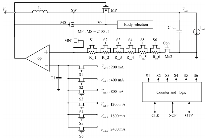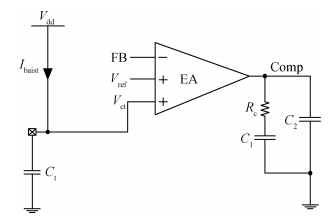
Fig. 1.
Schematic of conventional start-up technique.
SEMICONDUCTOR INTEGRATED CIRCUITS
Guoding Dai1, 2, , Wenliang Xiu1, Yuezhi Liu1, Yawei Qi1 and Zuqi Dong1
Corresponding author: Dai Guoding, Email: gddai@mail.xidian.edu.cn
Abstract: This paper presents a load adaptive soft-start scheme through which the inductor current of the synchronous boost DC-DC converter can trace the load current at the start-up stage. This scheme effectively eliminates the inrush-current and over-shoot voltage and improves the load capability of the converter. According to the output voltage, the start-up process is divided into three phases and at each phase the inductor current is limited to match the load. In the pre-charge phase, a step-increasing constant current gives a smooth rise of the output voltage which avoids inrush current and ensures the converter successfully starts up at different load situations. An additional ring oscillator operation phase enables the converter to start up as low as 1.4 V. When the converter enters into the system loop soft-start phase, an output voltage and inductor current detection methods make the transition of the phases smooth and the inductor current and output voltage rise steadily. Effective protection circuits such as short-circuit protection, current limit circuit and over-temperature protection circuit are designed to guarantee the safety and reliability of the chip during the start-up process. The proposed start-up circuit is implemented in a synchronous boost DC-DC converter based on TSMC 0.35μm CMOS process with an input voltage range 1.4-4.2 V, and a steady output voltage 5 V, and the switching frequency is 1 MHz. Simulation results show that inrush current and overshoot voltage are suppressed with a load range from 0-2.1 A, and inductor current is as low as 259 mA when the output shorts to the ground.
Keywords: load adaptive, soft-start scheme, synchronous boost DC-DC converter
| [1] |
Man T Y, Mok P K T, Chan M J. A 0.9 V input discontinuous conduction mode boost converter with CMOS-control rectifier. IEEE J Solid-State Circuits, 2008, 43(9): 2036 doi: 10.1109/JSSC.2008.2001933
|
| [2] |
Hsieh C Y, Chuang Y C, Chen K H. A novel precise step-shaped soft-start technique for integrated DC-DC converter. IEEE 14th International Conference on Electronics, Circuits and Systems, 2007: 771 http://cn.bing.com/academic/profile?id=2156697568&encoded=0&v=paper_preview&mkt=zh-cn
|
| [3] |
Le H P, Chae C S, Lee K C, et al. A single-inductor switching DC-DC converter with five outputs and ordered power-distributive control. IEEE J Solid-State Circuits, 2008, 42(12): 2706 http://cn.bing.com/academic/profile?id=2113514065&encoded=0&v=paper_preview&mkt=zh-cn
|
| [4] |
Lion W R, Yeh M L. Monolithic low-EMI CMOS DC-DC boost converter for portable applications. IEEE Trans Very Large Scale Integr Syst, 2014, 22(2): 420 doi: 10.1109/TVLSI.2013.2243927
|
| [5] |
Liou W R, Chen P H, Tzeng J C. A synchronous boost regulator with PWM/PFM mode operation. IEEE 8th International Conference on ASIC, 2009: 1066 http://cn.bing.com/academic/profile?id=2024065750&encoded=0&v=paper_preview&mkt=zh-cn
|
| [6] |
Shibata K, Lee H. A DC-DC converter using a high speed soft-start control circuit. IEEE International Symposium on Circuits and Systems, 2010, 109(2): 833 http://cn.bing.com/academic/profile?id=2019627317&encoded=0&v=paper_preview&mkt=zh-cn
|
| [7] |
Shyoukh M A, Lee H. A compact fully-integrated extremum-selector-based soft-start circuit for voltage regulators in bulk CMOS technologies. IEEE Trans Circuits Syst II, 2010, 57(10): 818 doi: 10.1109/TCSII.2010.2058597
|
| [8] |
Analog Devices Incorporated. 650 KHz/1.3 MHz step-up PWM DC-to-DC switching converter with 2.0 A current limit. Analog Devices Incorporated Datasheet ADP1613, available online in http://www.analog.com/media/en/technical-documentation/data-sheets/ADP1612_1613.pdf
|
| [9] |
Yang Weidong, Zang Jiandong, Li Tiehu, et al. A 16 b 2 GHz digital-to-analog converter in 0.18 μm CMOS with digital calibration technology. Journal of Semiconductors, 2015, 36(10): 105002 doi: 10.1088/1674-4926/36/10/105002
|
| [10] |
Wang Qing, Chen Ning, Xu Shen, et al. A novel trajectory prediction control for proximate time-optimal digital control DC-DC converters. Journal of Semiconductors, 2014, 35(9): 095010 doi: 10.1088/1674-4926/35/9/095010
|
| [11] |
Texas Instrument Incorporated. High voltage DC/DC boost converter with 0.5-A/1.3-A integrated switch. Texas Instrument Incorporated Datasheet TPS61081, available online in http://www.ti.com/lit/gpn/tps61086.pdf
|
| [12] |
Monolithic Power System Incorporated. 1.3 A fixed frequency white LED driver. Monolithic Power System Incorporated Datasheet MPS3202, available online in http://space.ednchina.com/ewebeditor/uploadfile/20110705085426780.pdf
|
| [13] |
Ribellino C, Milazzo P. Switch-type voltage regulator with reduction of occupied space for soft-start functions. United States Patent, 2003/6552517, 2003
|
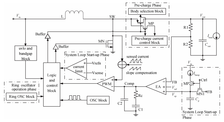
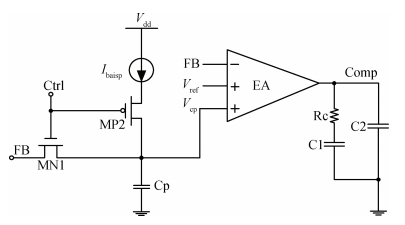
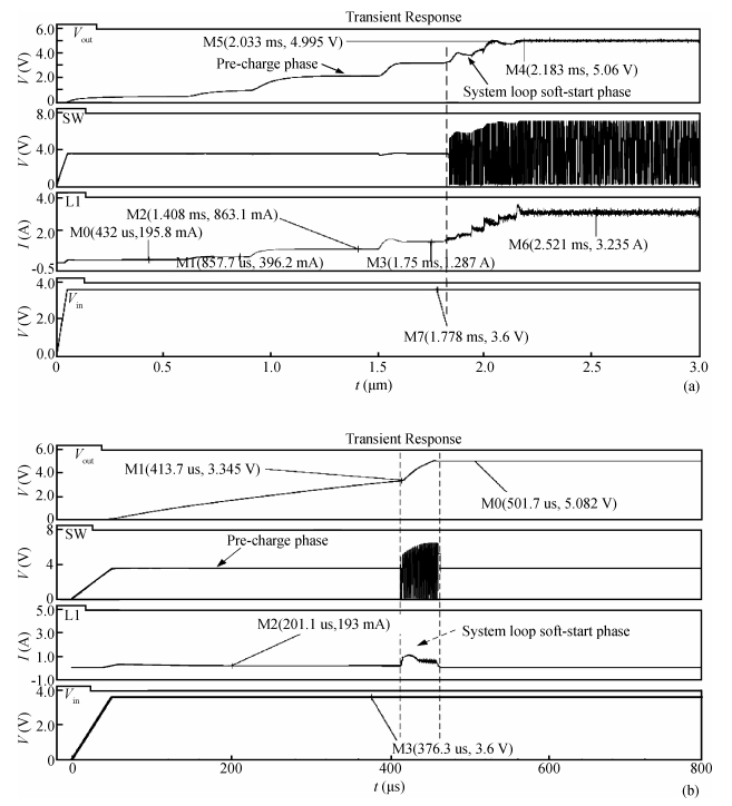
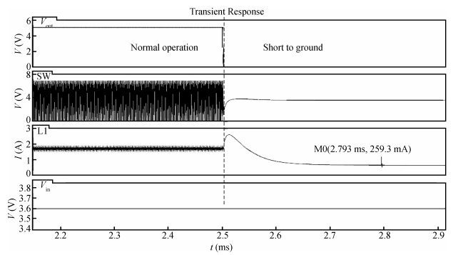
Table 1. Start-up phases for the boost DC-DC converter.
 |
Table 2. Pre-charge time in the extreme conditions.
 |
Table 3. Situations and corresponding operations in pre-charge phase.
 |
Table 4. Performance summary.
 |
| [1] |
Man T Y, Mok P K T, Chan M J. A 0.9 V input discontinuous conduction mode boost converter with CMOS-control rectifier. IEEE J Solid-State Circuits, 2008, 43(9): 2036 doi: 10.1109/JSSC.2008.2001933
|
| [2] |
Hsieh C Y, Chuang Y C, Chen K H. A novel precise step-shaped soft-start technique for integrated DC-DC converter. IEEE 14th International Conference on Electronics, Circuits and Systems, 2007: 771 http://cn.bing.com/academic/profile?id=2156697568&encoded=0&v=paper_preview&mkt=zh-cn
|
| [3] |
Le H P, Chae C S, Lee K C, et al. A single-inductor switching DC-DC converter with five outputs and ordered power-distributive control. IEEE J Solid-State Circuits, 2008, 42(12): 2706 http://cn.bing.com/academic/profile?id=2113514065&encoded=0&v=paper_preview&mkt=zh-cn
|
| [4] |
Lion W R, Yeh M L. Monolithic low-EMI CMOS DC-DC boost converter for portable applications. IEEE Trans Very Large Scale Integr Syst, 2014, 22(2): 420 doi: 10.1109/TVLSI.2013.2243927
|
| [5] |
Liou W R, Chen P H, Tzeng J C. A synchronous boost regulator with PWM/PFM mode operation. IEEE 8th International Conference on ASIC, 2009: 1066 http://cn.bing.com/academic/profile?id=2024065750&encoded=0&v=paper_preview&mkt=zh-cn
|
| [6] |
Shibata K, Lee H. A DC-DC converter using a high speed soft-start control circuit. IEEE International Symposium on Circuits and Systems, 2010, 109(2): 833 http://cn.bing.com/academic/profile?id=2019627317&encoded=0&v=paper_preview&mkt=zh-cn
|
| [7] |
Shyoukh M A, Lee H. A compact fully-integrated extremum-selector-based soft-start circuit for voltage regulators in bulk CMOS technologies. IEEE Trans Circuits Syst II, 2010, 57(10): 818 doi: 10.1109/TCSII.2010.2058597
|
| [8] |
Analog Devices Incorporated. 650 KHz/1.3 MHz step-up PWM DC-to-DC switching converter with 2.0 A current limit. Analog Devices Incorporated Datasheet ADP1613, available online in http://www.analog.com/media/en/technical-documentation/data-sheets/ADP1612_1613.pdf
|
| [9] |
Yang Weidong, Zang Jiandong, Li Tiehu, et al. A 16 b 2 GHz digital-to-analog converter in 0.18 μm CMOS with digital calibration technology. Journal of Semiconductors, 2015, 36(10): 105002 doi: 10.1088/1674-4926/36/10/105002
|
| [10] |
Wang Qing, Chen Ning, Xu Shen, et al. A novel trajectory prediction control for proximate time-optimal digital control DC-DC converters. Journal of Semiconductors, 2014, 35(9): 095010 doi: 10.1088/1674-4926/35/9/095010
|
| [11] |
Texas Instrument Incorporated. High voltage DC/DC boost converter with 0.5-A/1.3-A integrated switch. Texas Instrument Incorporated Datasheet TPS61081, available online in http://www.ti.com/lit/gpn/tps61086.pdf
|
| [12] |
Monolithic Power System Incorporated. 1.3 A fixed frequency white LED driver. Monolithic Power System Incorporated Datasheet MPS3202, available online in http://space.ednchina.com/ewebeditor/uploadfile/20110705085426780.pdf
|
| [13] |
Ribellino C, Milazzo P. Switch-type voltage regulator with reduction of occupied space for soft-start functions. United States Patent, 2003/6552517, 2003
|


Article views: 3718 Times PDF downloads: 49 Times Cited by: 0 Times
Received: 04 November 2015 Revised: 26 April 2016 Online: Published: 01 October 2016
| Citation: |
Guoding Dai, Wenliang Xiu, Yuezhi Liu, Yawei Qi, Zuqi Dong. Load adaptive start-up scheme for synchronous boost DC-DC converter[J]. Journal of Semiconductors, 2016, 37(10): 105002. doi: 10.1088/1674-4926/37/10/105002
****
G D Dai, W L Xiu, Y Z Liu, Y W Qi, Z Q Dong. Load adaptive start-up scheme for synchronous boost DC-DC converter[J]. J. Semicond., 2016, 37(10): 105002. doi: 10.1088/1674-4926/37/10/105002.

|
| [1] |
Man T Y, Mok P K T, Chan M J. A 0.9 V input discontinuous conduction mode boost converter with CMOS-control rectifier. IEEE J Solid-State Circuits, 2008, 43(9): 2036 doi: 10.1109/JSSC.2008.2001933
|
| [2] |
Hsieh C Y, Chuang Y C, Chen K H. A novel precise step-shaped soft-start technique for integrated DC-DC converter. IEEE 14th International Conference on Electronics, Circuits and Systems, 2007: 771 http://cn.bing.com/academic/profile?id=2156697568&encoded=0&v=paper_preview&mkt=zh-cn
|
| [3] |
Le H P, Chae C S, Lee K C, et al. A single-inductor switching DC-DC converter with five outputs and ordered power-distributive control. IEEE J Solid-State Circuits, 2008, 42(12): 2706 http://cn.bing.com/academic/profile?id=2113514065&encoded=0&v=paper_preview&mkt=zh-cn
|
| [4] |
Lion W R, Yeh M L. Monolithic low-EMI CMOS DC-DC boost converter for portable applications. IEEE Trans Very Large Scale Integr Syst, 2014, 22(2): 420 doi: 10.1109/TVLSI.2013.2243927
|
| [5] |
Liou W R, Chen P H, Tzeng J C. A synchronous boost regulator with PWM/PFM mode operation. IEEE 8th International Conference on ASIC, 2009: 1066 http://cn.bing.com/academic/profile?id=2024065750&encoded=0&v=paper_preview&mkt=zh-cn
|
| [6] |
Shibata K, Lee H. A DC-DC converter using a high speed soft-start control circuit. IEEE International Symposium on Circuits and Systems, 2010, 109(2): 833 http://cn.bing.com/academic/profile?id=2019627317&encoded=0&v=paper_preview&mkt=zh-cn
|
| [7] |
Shyoukh M A, Lee H. A compact fully-integrated extremum-selector-based soft-start circuit for voltage regulators in bulk CMOS technologies. IEEE Trans Circuits Syst II, 2010, 57(10): 818 doi: 10.1109/TCSII.2010.2058597
|
| [8] |
Analog Devices Incorporated. 650 KHz/1.3 MHz step-up PWM DC-to-DC switching converter with 2.0 A current limit. Analog Devices Incorporated Datasheet ADP1613, available online in http://www.analog.com/media/en/technical-documentation/data-sheets/ADP1612_1613.pdf
|
| [9] |
Yang Weidong, Zang Jiandong, Li Tiehu, et al. A 16 b 2 GHz digital-to-analog converter in 0.18 μm CMOS with digital calibration technology. Journal of Semiconductors, 2015, 36(10): 105002 doi: 10.1088/1674-4926/36/10/105002
|
| [10] |
Wang Qing, Chen Ning, Xu Shen, et al. A novel trajectory prediction control for proximate time-optimal digital control DC-DC converters. Journal of Semiconductors, 2014, 35(9): 095010 doi: 10.1088/1674-4926/35/9/095010
|
| [11] |
Texas Instrument Incorporated. High voltage DC/DC boost converter with 0.5-A/1.3-A integrated switch. Texas Instrument Incorporated Datasheet TPS61081, available online in http://www.ti.com/lit/gpn/tps61086.pdf
|
| [12] |
Monolithic Power System Incorporated. 1.3 A fixed frequency white LED driver. Monolithic Power System Incorporated Datasheet MPS3202, available online in http://space.ednchina.com/ewebeditor/uploadfile/20110705085426780.pdf
|
| [13] |
Ribellino C, Milazzo P. Switch-type voltage regulator with reduction of occupied space for soft-start functions. United States Patent, 2003/6552517, 2003
|

 WeChat ID
Journal of Semiconductors © 2017 All Rights Reserved 京ICP备05085259号-2

 DownLoad: