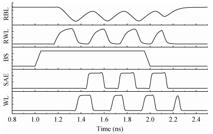
Fig. 1.
Traditional replica bit line control circuit.
SEMICONDUCTOR INTEGRATED CIRCUITS
Pengjun Wang, Keji Zhou, Huihong Zhang and Daohui Gong
Corresponding author: Wang Pengjun, Email:wangpengjun@nbu.edu.cn
Abstract: A design of a replica bit line control circuit to optimize power for SRAM is proposed. The proposed design overcomes the limitations of the traditional replica bit line control circuit, which cannot shut off the word line in time. In the novel design, the delay of word line enable and disable paths are balanced. Thus, the word line can be opened and shut off in time. Moreover, the chip select signal is decomposed, which prevents feedback oscillations caused by the replica bit line and the replica word line. As a result, the switch power caused by unnecessary discharging of the bit line is reduced. A 2-kb SRAM is fully custom designed in an SMIC 65-nm CMOS process. The traditional replica bit line control circuit and the new replica bit line control circuit are used in the designed SRAM, and their performances are compared with each other. The experimental results show that at a supply voltage of 1.2 V, the switch power consumption of the memory array can be reduced by 53.7%.
Keywords: low power, static random access memory (SRAM), replica bit line control circuit, circuit design
| [1] |
Alioto M. Ultra-low power VLSI circuit design demystified and explained: a tutorial. IEEE Trans Circuits Syst I, 2012, 59(1): 3 doi: 10.1109/TCSI.2011.2177004
|
| [2] |
Yang Q K, Wang P J, Zheng X S. Design of ternary counter based on adiabatic domino circuit. Journal of Electronics (China), 2013, 30(1): 104 doi: 10.1007/s11767-013-2134-2
|
| [3] |
Cai Jiangzheng, Zhang Sumin, Yuan Jia, et al. A 320 mV, 6 kb subthreshold 10T SRAM employing voltage lowering techniques. Journal of Semiconductors, 2015, 36(6): 065007 doi: 10.1088/1674-4926/36/6/065007
|
| [4] |
Sinangil M E, Chandrakasan A P. Application-specific SRAM design using output prediction to reduce bit-line switching activity and statistically gated sense amplifiers for up to 1.9 lower energy/access. IEEE J Solid-State Circuits, 2014, 49(1): 107 doi: 10.1109/JSSC.2013.2280310
|
| [5] |
Pasandi G, Mehrabi K, Fakhraie S M. A new low-power SRAM block suitable for applications with normal data distribution. Iranian Conference on Electrical Engineering, 2015: 1316 https://www.researchgate.net/profile/Ghasem_Pasandi/publication/281243220_A_New_Low-Power_SRAM_Block_Suitable_for_Applications_with_Normal_Data_Distribution/links/55f951f608aeafc8ac224404.pdf?origin=publication_detail
|
| [6] |
Na T, Woo S H, Kim J, et al. Comparative study of various latch-type sense amplifiers. IEEE Trans Very Large Scale Integr Syst, 2014, 22(2): 425 doi: 10.1109/TVLSI.2013.2239320
|
| [7] |
Arandilla C D C, Madamba J A R. Comparison of replica bitline technique and chain delay technique as read timing control for low-power asynchronous SRAM. 2011 Fifth Asia Modelling Symposium, 2011: 275 http://cn.bing.com/academic/profile?id=2346687240&encoded=0&v=paper_preview&mkt=zh-cn
|
| [8] |
Amrutur B S, Horowitz M. A replica technique for wordline and sense control in low-power SRAM's. IEEE J Solid-State Circuits, 1998, 33(8): 1208 doi: 10.1109/4.705359
|
| [9] |
Lu W, Peng C, Tao Y, et al. Efficient replica bitline technique for variation-tolerant timing generation scheme of SRAM sense amplifiers. Electron Lett, 2015, 51(10): 742 doi: 10.1049/el.2015.0574
|
| [10] |
Niki Y, Kawasumi A, Suzuki A, et al. A digitized replica bitline delay technique for random-variation-tolerant timing generation of SRAM sense amplifiers. IEEE J Solid-State Circuits, 2011, 46(11): 2545 doi: 10.1109/JSSC.2011.2164294
|
| [11] |
Wu J H, Zhu J F, Xia Y C, et al. A multiple-stage parallel replica-bitline delay addition technique for reducing timing variation of SRAM sense amplifiers. IEEE Trans Circuits Syst II, 2014, 61(4): 264 doi: 10.1109/TCSII.2014.2304893
|
| [12] |
Abu-Rahma M H, Anis M, Yoon S S. Reducing SRAM power using fine-grained wordline pulsewidth control. IEEE Trans Very Large Scale Integr Syst, 2010, 18(3): 356 doi: 10.1109/TVLSI.2009.2012511
|
| [13] |
Wang Y, Ahn H, Bhattacharya U, et al. A 1.1 GHz 12 μA/Mb-leakage SRAM design in 65 nm ultra-low-power CMOS technology with integrated leakage reduction for mobile applications. IEEE J Solid-State Circuits, 2008, 43(1): 172 doi: 10.1109/JSSC.2007.907996
|
| [14] |
Karl E, Wang Y, Ng Y G, et al. A 4.6 GHz 162 Mb SRAM design in 22 nm tri-gate CMOS technology with integrated active VMIN-enhancing assist circuitry. IEEE International Solid-State Circuits Conference Digest of Technical Papers, 2012: 230232 http://cn.bing.com/academic/profile?id=2015854837&encoded=0&v=paper_preview&mkt=zh-cn
|
| [15] |
Ding Lili, Yao Zhibin, Guo Hongxia, et al, Worst-case total dose radiation effect in deep-submicron SRAM circuits. Journal of Semiconductors, 2012, 33(7): 075010 doi: 10.1088/1674-4926/33/7/075010
|
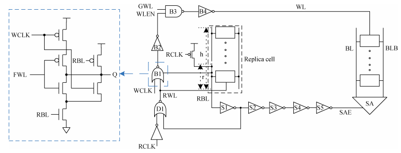

Table 1. Performance comparison of replica bit line control circuit.

|
| [1] |
Alioto M. Ultra-low power VLSI circuit design demystified and explained: a tutorial. IEEE Trans Circuits Syst I, 2012, 59(1): 3 doi: 10.1109/TCSI.2011.2177004
|
| [2] |
Yang Q K, Wang P J, Zheng X S. Design of ternary counter based on adiabatic domino circuit. Journal of Electronics (China), 2013, 30(1): 104 doi: 10.1007/s11767-013-2134-2
|
| [3] |
Cai Jiangzheng, Zhang Sumin, Yuan Jia, et al. A 320 mV, 6 kb subthreshold 10T SRAM employing voltage lowering techniques. Journal of Semiconductors, 2015, 36(6): 065007 doi: 10.1088/1674-4926/36/6/065007
|
| [4] |
Sinangil M E, Chandrakasan A P. Application-specific SRAM design using output prediction to reduce bit-line switching activity and statistically gated sense amplifiers for up to 1.9 lower energy/access. IEEE J Solid-State Circuits, 2014, 49(1): 107 doi: 10.1109/JSSC.2013.2280310
|
| [5] |
Pasandi G, Mehrabi K, Fakhraie S M. A new low-power SRAM block suitable for applications with normal data distribution. Iranian Conference on Electrical Engineering, 2015: 1316 https://www.researchgate.net/profile/Ghasem_Pasandi/publication/281243220_A_New_Low-Power_SRAM_Block_Suitable_for_Applications_with_Normal_Data_Distribution/links/55f951f608aeafc8ac224404.pdf?origin=publication_detail
|
| [6] |
Na T, Woo S H, Kim J, et al. Comparative study of various latch-type sense amplifiers. IEEE Trans Very Large Scale Integr Syst, 2014, 22(2): 425 doi: 10.1109/TVLSI.2013.2239320
|
| [7] |
Arandilla C D C, Madamba J A R. Comparison of replica bitline technique and chain delay technique as read timing control for low-power asynchronous SRAM. 2011 Fifth Asia Modelling Symposium, 2011: 275 http://cn.bing.com/academic/profile?id=2346687240&encoded=0&v=paper_preview&mkt=zh-cn
|
| [8] |
Amrutur B S, Horowitz M. A replica technique for wordline and sense control in low-power SRAM's. IEEE J Solid-State Circuits, 1998, 33(8): 1208 doi: 10.1109/4.705359
|
| [9] |
Lu W, Peng C, Tao Y, et al. Efficient replica bitline technique for variation-tolerant timing generation scheme of SRAM sense amplifiers. Electron Lett, 2015, 51(10): 742 doi: 10.1049/el.2015.0574
|
| [10] |
Niki Y, Kawasumi A, Suzuki A, et al. A digitized replica bitline delay technique for random-variation-tolerant timing generation of SRAM sense amplifiers. IEEE J Solid-State Circuits, 2011, 46(11): 2545 doi: 10.1109/JSSC.2011.2164294
|
| [11] |
Wu J H, Zhu J F, Xia Y C, et al. A multiple-stage parallel replica-bitline delay addition technique for reducing timing variation of SRAM sense amplifiers. IEEE Trans Circuits Syst II, 2014, 61(4): 264 doi: 10.1109/TCSII.2014.2304893
|
| [12] |
Abu-Rahma M H, Anis M, Yoon S S. Reducing SRAM power using fine-grained wordline pulsewidth control. IEEE Trans Very Large Scale Integr Syst, 2010, 18(3): 356 doi: 10.1109/TVLSI.2009.2012511
|
| [13] |
Wang Y, Ahn H, Bhattacharya U, et al. A 1.1 GHz 12 μA/Mb-leakage SRAM design in 65 nm ultra-low-power CMOS technology with integrated leakage reduction for mobile applications. IEEE J Solid-State Circuits, 2008, 43(1): 172 doi: 10.1109/JSSC.2007.907996
|
| [14] |
Karl E, Wang Y, Ng Y G, et al. A 4.6 GHz 162 Mb SRAM design in 22 nm tri-gate CMOS technology with integrated active VMIN-enhancing assist circuitry. IEEE International Solid-State Circuits Conference Digest of Technical Papers, 2012: 230232 http://cn.bing.com/academic/profile?id=2015854837&encoded=0&v=paper_preview&mkt=zh-cn
|
| [15] |
Ding Lili, Yao Zhibin, Guo Hongxia, et al, Worst-case total dose radiation effect in deep-submicron SRAM circuits. Journal of Semiconductors, 2012, 33(7): 075010 doi: 10.1088/1674-4926/33/7/075010
|


Article views: 5180 Times PDF downloads: 182 Times Cited by: 0 Times
Received: 23 April 2016 Revised: 24 June 2016 Online: Published: 01 December 2016
| Citation: |
Pengjun Wang, Keji Zhou, Huihong Zhang, Daohui Gong. Design of replica bit line control circuit to optimize power for SRAM[J]. Journal of Semiconductors, 2016, 37(12): 125002. doi: 10.1088/1674-4926/37/12/125002
****
P J Wang, K J Zhou, H H Zhang, D H Gong. Design of replica bit line control circuit to optimize power for SRAM[J]. J. Semicond., 2016, 37(12): 125002. doi: 10.1088/1674-4926/37/12/125002.

|
| [1] |
Alioto M. Ultra-low power VLSI circuit design demystified and explained: a tutorial. IEEE Trans Circuits Syst I, 2012, 59(1): 3 doi: 10.1109/TCSI.2011.2177004
|
| [2] |
Yang Q K, Wang P J, Zheng X S. Design of ternary counter based on adiabatic domino circuit. Journal of Electronics (China), 2013, 30(1): 104 doi: 10.1007/s11767-013-2134-2
|
| [3] |
Cai Jiangzheng, Zhang Sumin, Yuan Jia, et al. A 320 mV, 6 kb subthreshold 10T SRAM employing voltage lowering techniques. Journal of Semiconductors, 2015, 36(6): 065007 doi: 10.1088/1674-4926/36/6/065007
|
| [4] |
Sinangil M E, Chandrakasan A P. Application-specific SRAM design using output prediction to reduce bit-line switching activity and statistically gated sense amplifiers for up to 1.9 lower energy/access. IEEE J Solid-State Circuits, 2014, 49(1): 107 doi: 10.1109/JSSC.2013.2280310
|
| [5] |
Pasandi G, Mehrabi K, Fakhraie S M. A new low-power SRAM block suitable for applications with normal data distribution. Iranian Conference on Electrical Engineering, 2015: 1316 https://www.researchgate.net/profile/Ghasem_Pasandi/publication/281243220_A_New_Low-Power_SRAM_Block_Suitable_for_Applications_with_Normal_Data_Distribution/links/55f951f608aeafc8ac224404.pdf?origin=publication_detail
|
| [6] |
Na T, Woo S H, Kim J, et al. Comparative study of various latch-type sense amplifiers. IEEE Trans Very Large Scale Integr Syst, 2014, 22(2): 425 doi: 10.1109/TVLSI.2013.2239320
|
| [7] |
Arandilla C D C, Madamba J A R. Comparison of replica bitline technique and chain delay technique as read timing control for low-power asynchronous SRAM. 2011 Fifth Asia Modelling Symposium, 2011: 275 http://cn.bing.com/academic/profile?id=2346687240&encoded=0&v=paper_preview&mkt=zh-cn
|
| [8] |
Amrutur B S, Horowitz M. A replica technique for wordline and sense control in low-power SRAM's. IEEE J Solid-State Circuits, 1998, 33(8): 1208 doi: 10.1109/4.705359
|
| [9] |
Lu W, Peng C, Tao Y, et al. Efficient replica bitline technique for variation-tolerant timing generation scheme of SRAM sense amplifiers. Electron Lett, 2015, 51(10): 742 doi: 10.1049/el.2015.0574
|
| [10] |
Niki Y, Kawasumi A, Suzuki A, et al. A digitized replica bitline delay technique for random-variation-tolerant timing generation of SRAM sense amplifiers. IEEE J Solid-State Circuits, 2011, 46(11): 2545 doi: 10.1109/JSSC.2011.2164294
|
| [11] |
Wu J H, Zhu J F, Xia Y C, et al. A multiple-stage parallel replica-bitline delay addition technique for reducing timing variation of SRAM sense amplifiers. IEEE Trans Circuits Syst II, 2014, 61(4): 264 doi: 10.1109/TCSII.2014.2304893
|
| [12] |
Abu-Rahma M H, Anis M, Yoon S S. Reducing SRAM power using fine-grained wordline pulsewidth control. IEEE Trans Very Large Scale Integr Syst, 2010, 18(3): 356 doi: 10.1109/TVLSI.2009.2012511
|
| [13] |
Wang Y, Ahn H, Bhattacharya U, et al. A 1.1 GHz 12 μA/Mb-leakage SRAM design in 65 nm ultra-low-power CMOS technology with integrated leakage reduction for mobile applications. IEEE J Solid-State Circuits, 2008, 43(1): 172 doi: 10.1109/JSSC.2007.907996
|
| [14] |
Karl E, Wang Y, Ng Y G, et al. A 4.6 GHz 162 Mb SRAM design in 22 nm tri-gate CMOS technology with integrated active VMIN-enhancing assist circuitry. IEEE International Solid-State Circuits Conference Digest of Technical Papers, 2012: 230232 http://cn.bing.com/academic/profile?id=2015854837&encoded=0&v=paper_preview&mkt=zh-cn
|
| [15] |
Ding Lili, Yao Zhibin, Guo Hongxia, et al, Worst-case total dose radiation effect in deep-submicron SRAM circuits. Journal of Semiconductors, 2012, 33(7): 075010 doi: 10.1088/1674-4926/33/7/075010
|

 WeChat ID
Journal of Semiconductors © 2017 All Rights Reserved 京ICP备05085259号-2

 DownLoad: