


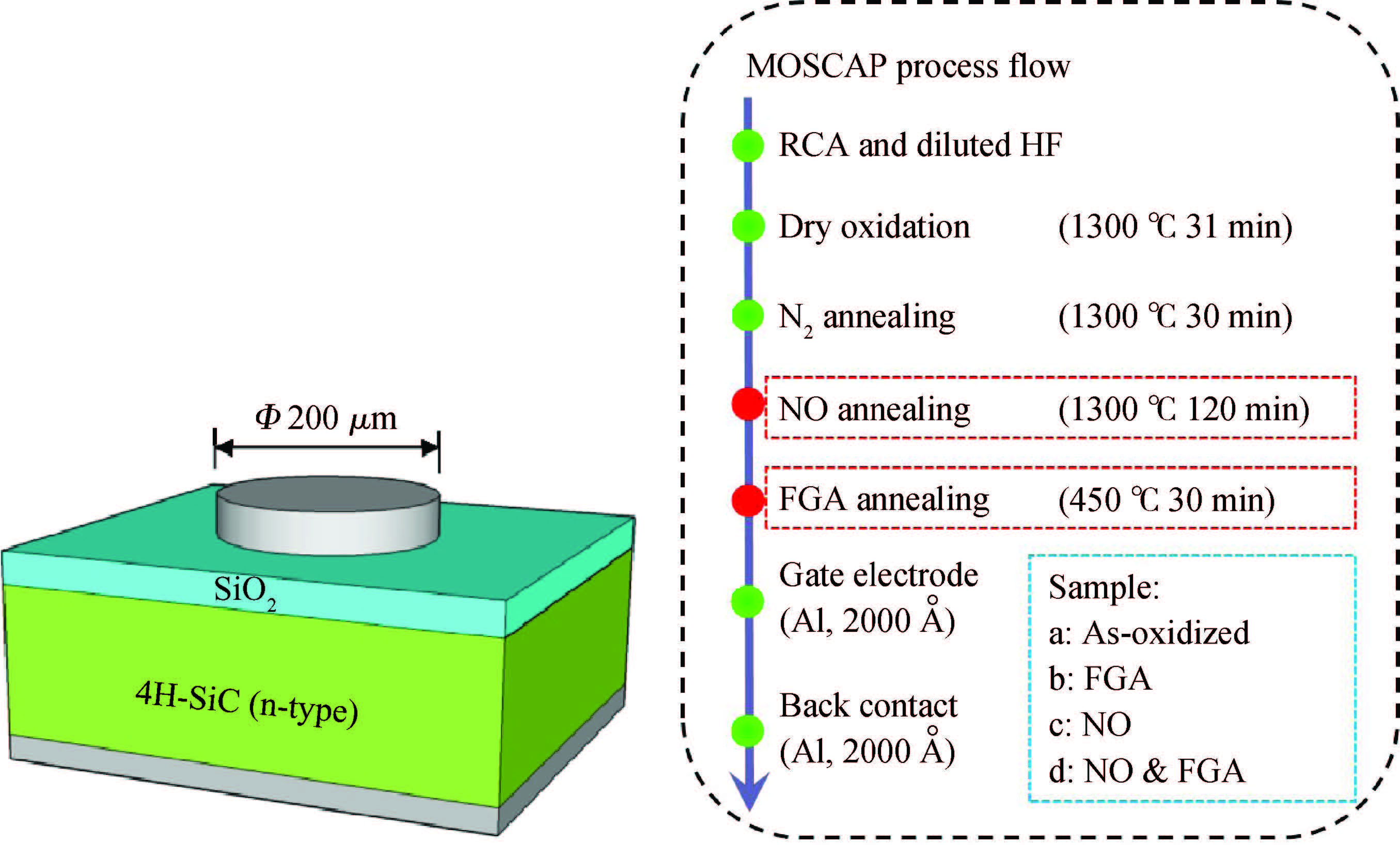
图 1.
4H-SiC MOS capacitor and its fabrication process flow. The post-oxidation treatments for each sample are also shown.
SEMICONDUCTOR TECHNOLOGY
Yiyu Wang1, 2, Zhaoyang Peng1, Huajun Shen1, , Chengzhan Li2, Jia Wu2, Yachao Tang1, Yanli Zhao2, Ximing Chen2, Kean Liu2 and Xinyu Liu1
Corresponding author: Huajun Shen, shenhuajun@ime.ac.cn
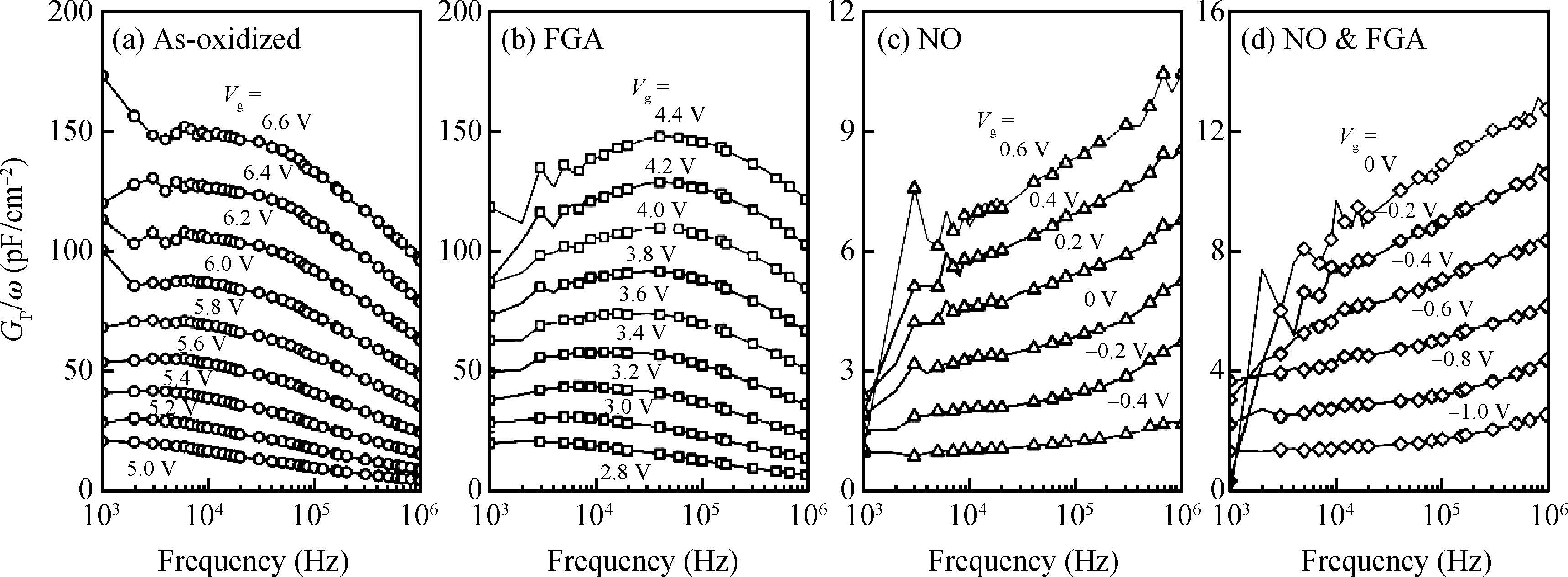
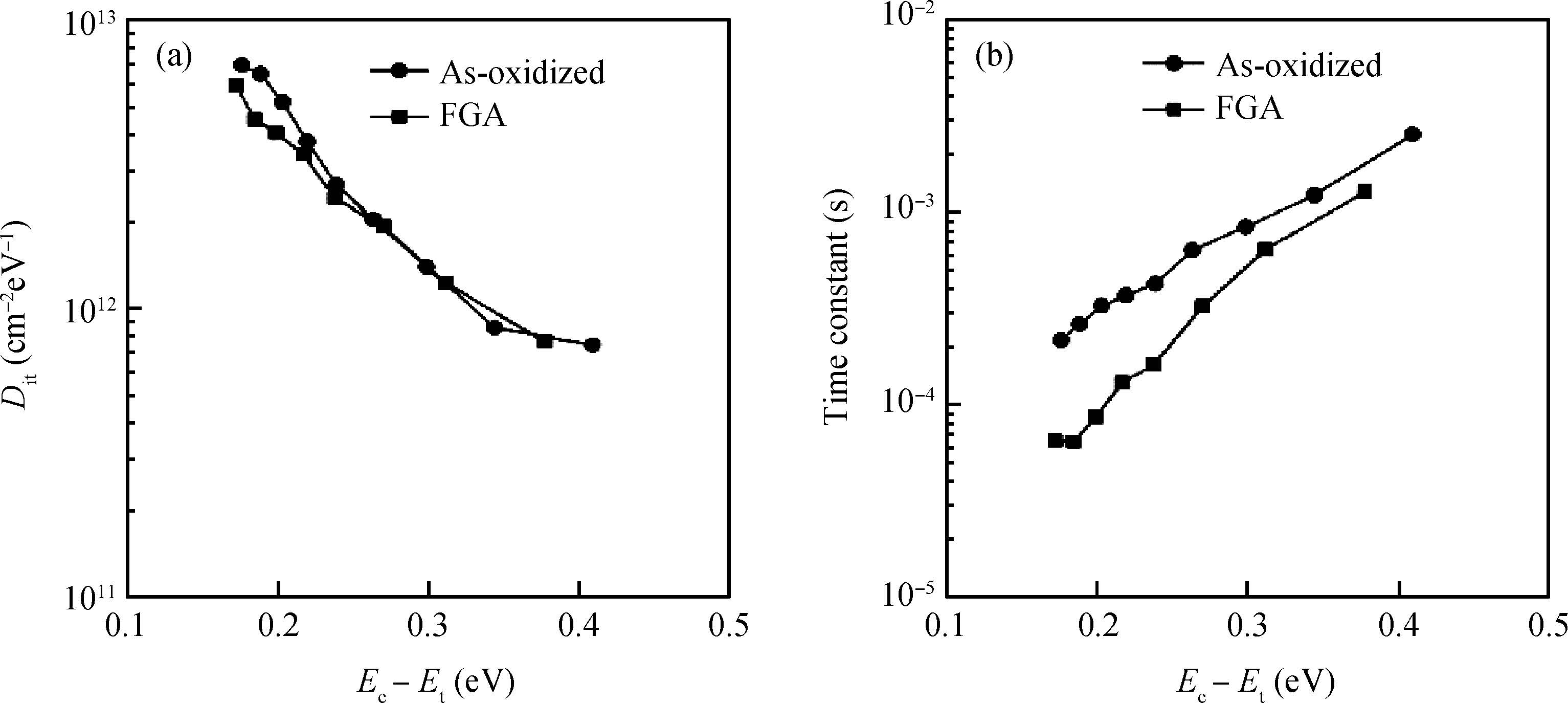
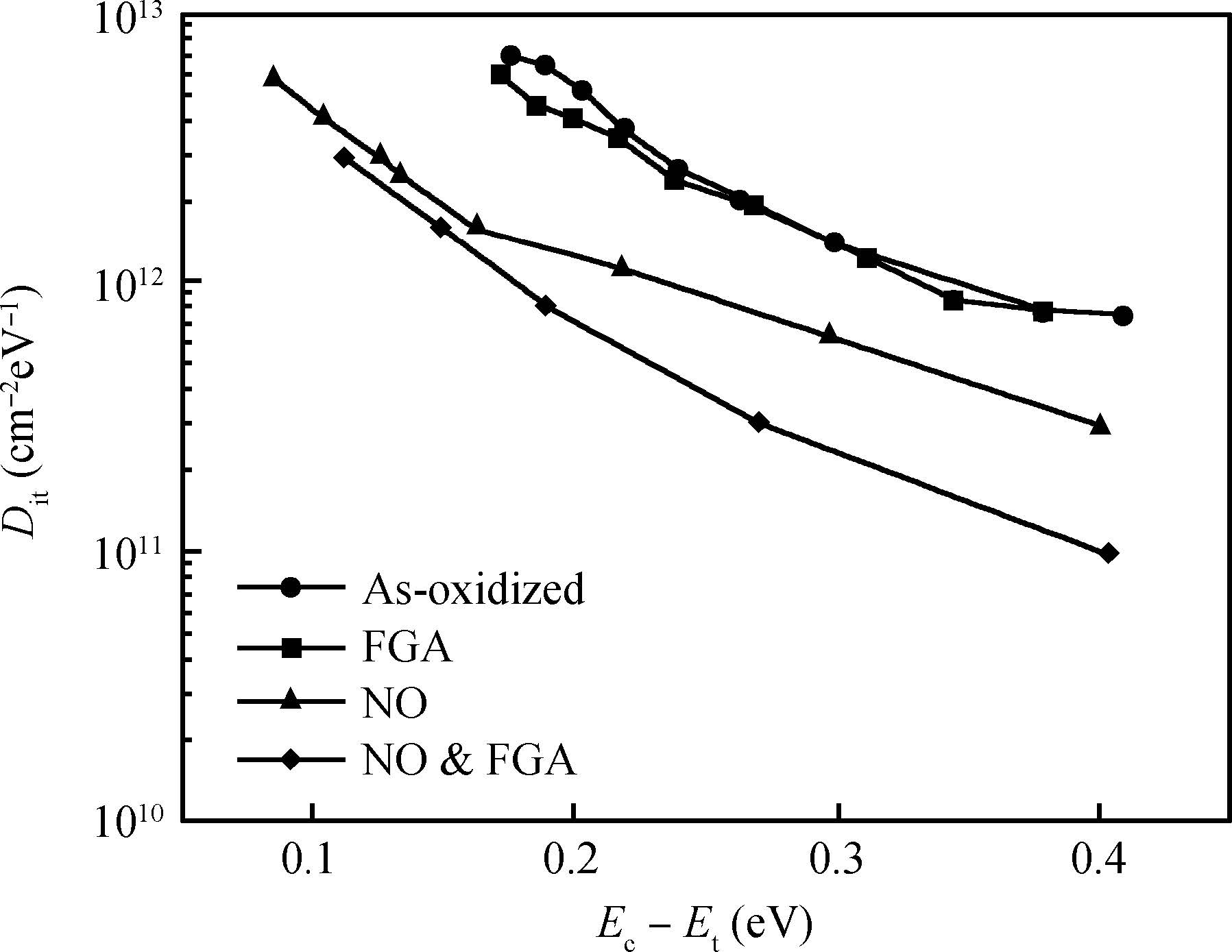
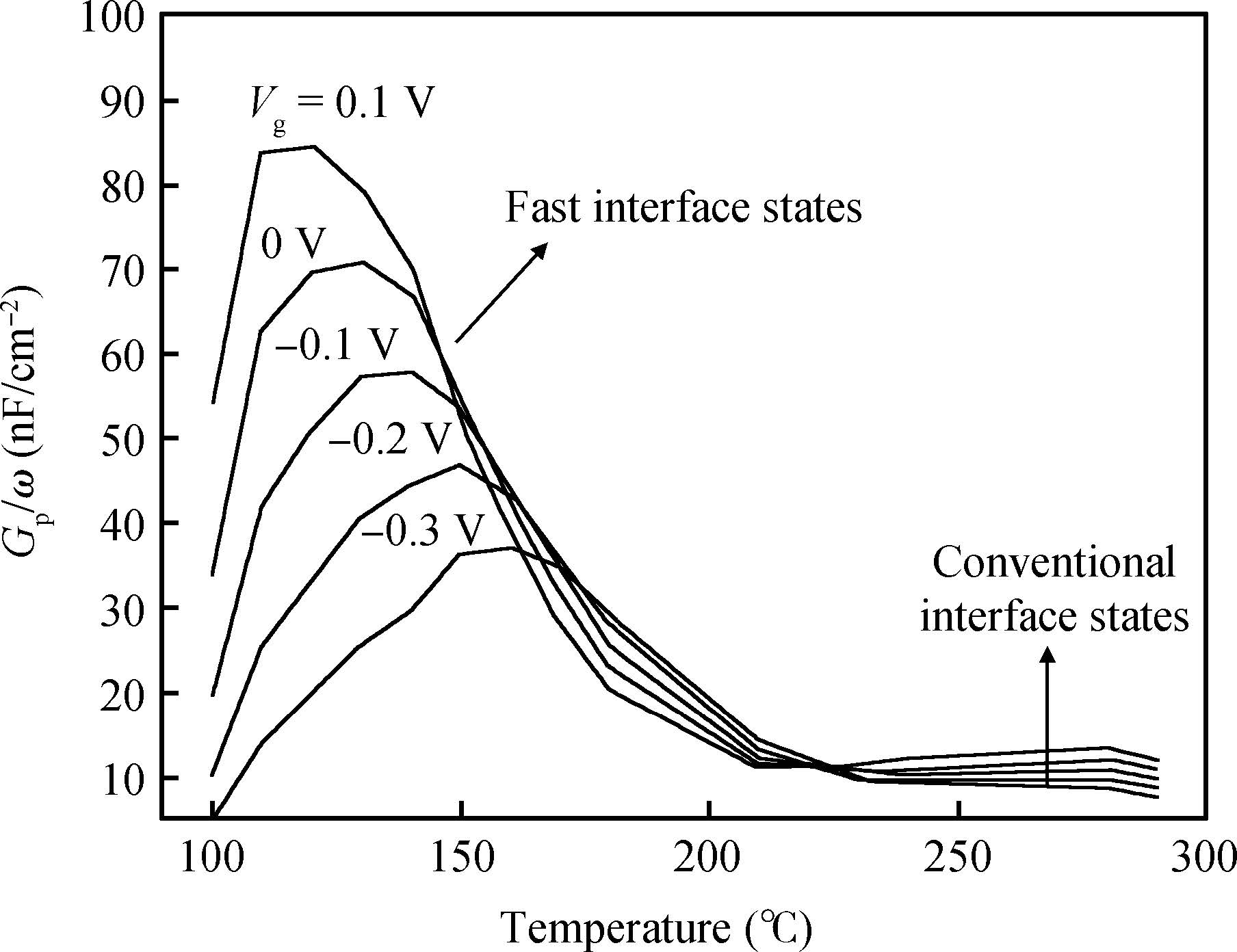
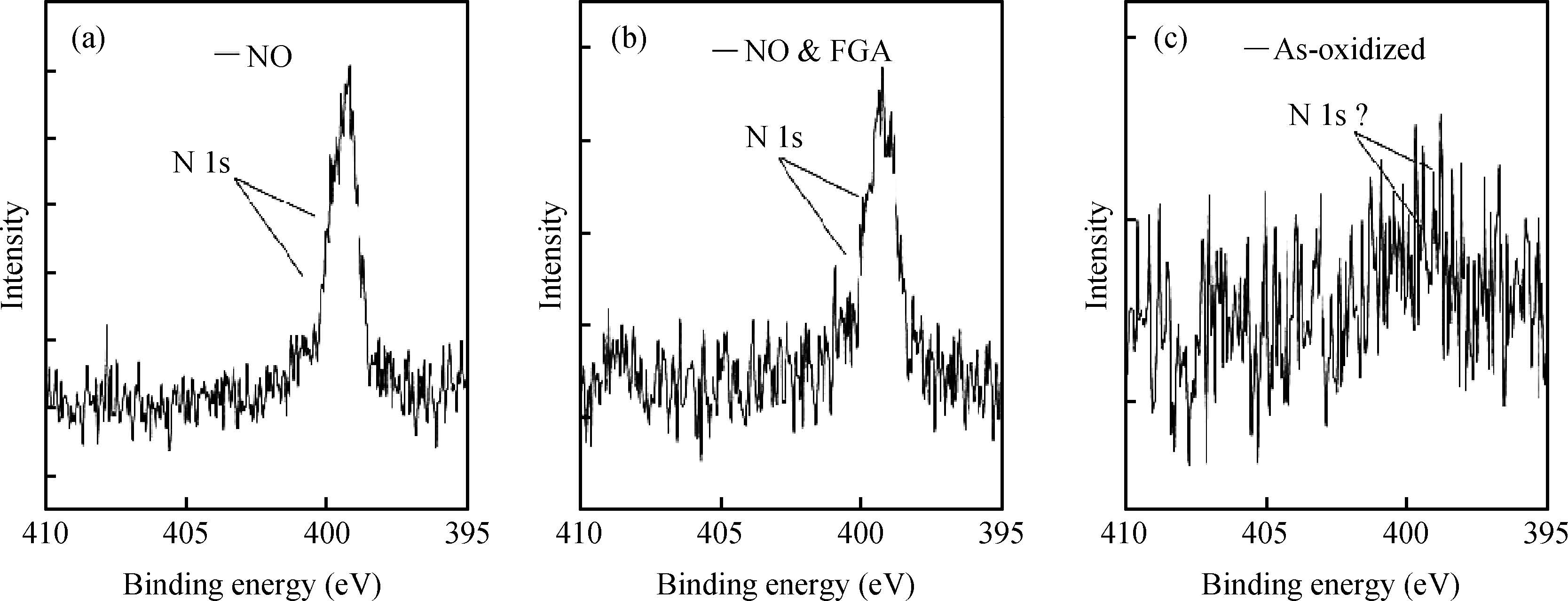
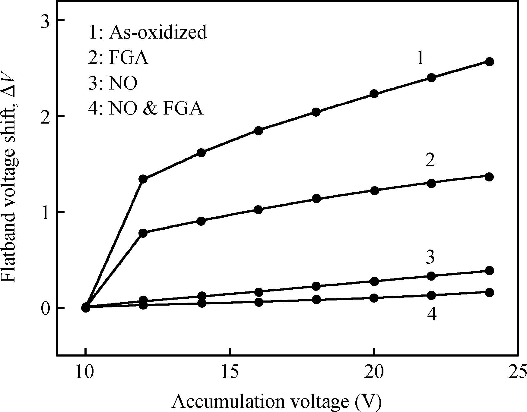
Abstract: We investigate the effects of NO annealing and forming gas (FG) annealing on the electrical properties of a SiO2/SiC interface by low-temperature conductance measurements. With nitrogen passivation, the density of interface states (DIT) is significantly reduced in the entire energy range, and the shift of flatband voltage, Δ VFB, is effectively suppressed to less than 0.4 V. However, very fast states are observed after NO annealing and the response frequencies are higher than 1 MHz at room temperature. After additional FG annealing, the DIT and Δ VFB are further reduced. The values of the DIT decrease to less than 1011 cm-2 eV-1 for the energy range of EC - ET ≥0.4 eV. It is suggested that the fast states in shallow energy levels originated from the N atoms accumulating at the interface by NO annealing. Though FG annealing has a limited effect on these shallow traps, hydrogen can terminate the residual Si and C dangling bonds corresponding to traps at deep energy levels and improve the interface quality further. It is indicated that NO annealing in conjunction with FG annealing will be a better post-oxidation process method for high performance SiC MOSFETs.
Keywords: SiO2/SiC interface, NO annealing, forming gas annealing, density of interface states
| [1] | |
| [2] | |
| [3] | |
| [4] | |
| [5] | |
| [6] | |
| [7] | |
| [8] | |
| [9] | |
| [10] | |
| [11] | |
| [12] | |
| [13] | |
| [14] | |
| [15] | |
| [16] | |
| [17] | |
| [18] | |
| [19] | |
| [20] | |
| [21] | |
| [22] | |
| [23] | |
| [24] | |
| [25] | |
| [26] | |
| [27] | |
| [28] | |
| [29] | |
| [30] | |
| [31] | |
| [32] | |
| [33] | |
| [34] | |
| [35] | |
| [36] | |
| [37] | |
| [38] | |
| [39] |


Article views: 3640 Times PDF downloads: 58 Times Cited by: 0 Times
Received: 22 May 2015 Revised: Online: Published: 01 February 2016
| Citation: |
Yiyu Wang, Zhaoyang Peng, Huajun Shen, Chengzhan Li, Jia Wu, Yachao Tang, Yanli Zhao, Ximing Chen, Kean Liu, Xinyu Liu. Characterization of the effects of nitrogen and hydrogen passivation on SiO2/4H-SiC interface by low temperature conductance measurements[J]. Journal of Semiconductors, 2016, 37(2): 026001. doi: 10.1088/1674-4926/37/2/026001
****
Y Y Wang, Z Y Peng, H J Shen, C Z Li, J Wu, Y C Tang, Y L Zhao, X M Chen, K A Liu, X Y Liu. Characterization of the effects of nitrogen and hydrogen passivation on SiO2/4H-SiC interface by low temperature conductance measurements[J]. J. Semicond., 2016, 37(2): 026001. doi: 10.1088/1674-4926/37/2/026001.

|
| [1] | |
| [2] | |
| [3] | |
| [4] | |
| [5] | |
| [6] | |
| [7] | |
| [8] | |
| [9] | |
| [10] | |
| [11] | |
| [12] | |
| [13] | |
| [14] | |
| [15] | |
| [16] | |
| [17] | |
| [18] | |
| [19] | |
| [20] | |
| [21] | |
| [22] | |
| [23] | |
| [24] | |
| [25] | |
| [26] | |
| [27] | |
| [28] | |
| [29] | |
| [30] | |
| [31] | |
| [32] | |
| [33] | |
| [34] | |
| [35] | |
| [36] | |
| [37] | |
| [38] | |
| [39] |

 WeChat ID
Journal of Semiconductors © 2017 All Rights Reserved 京ICP备05085259号-2

 DownLoad:

