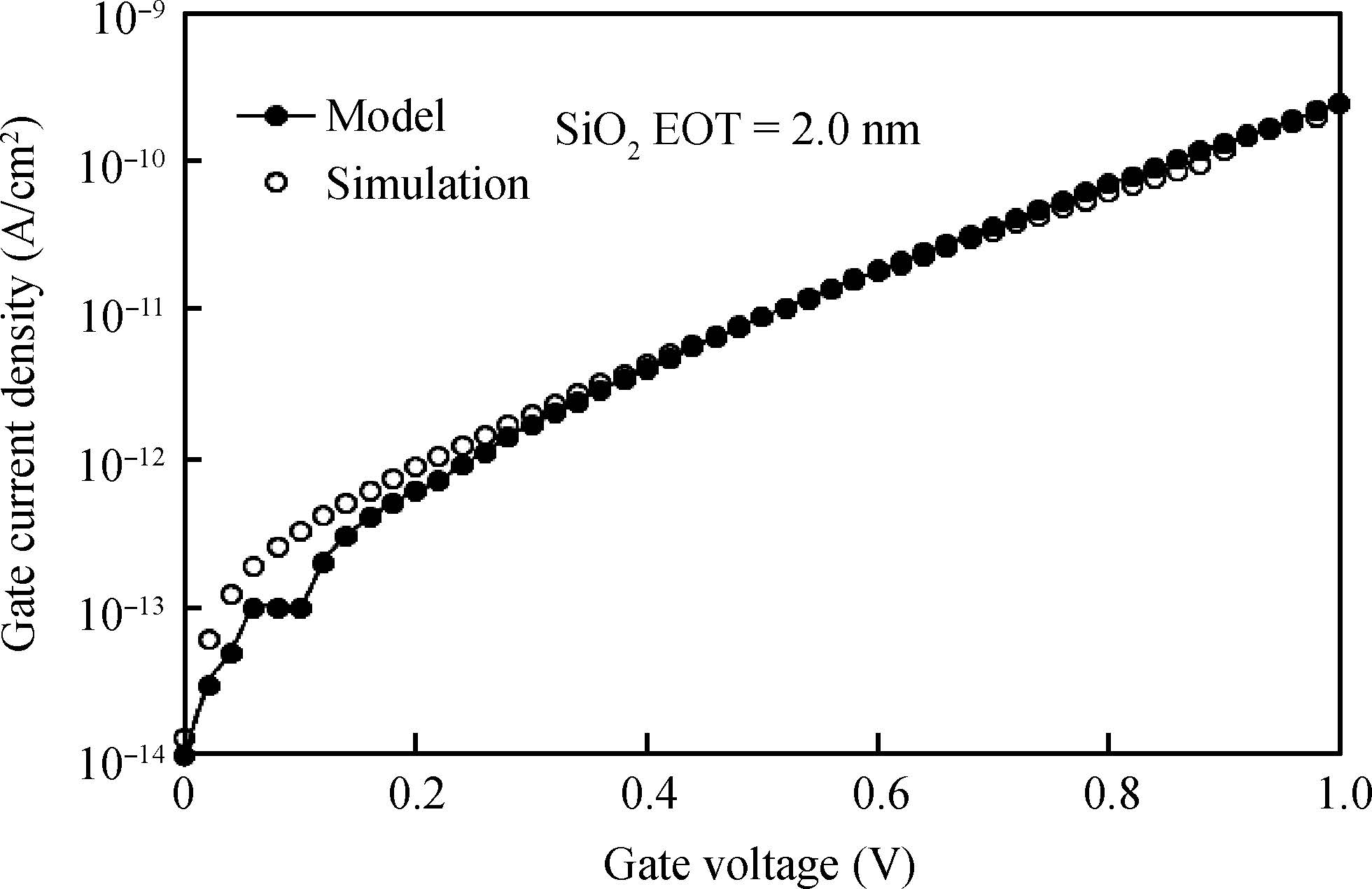
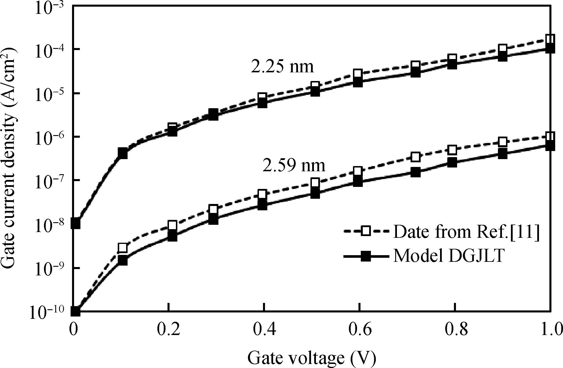
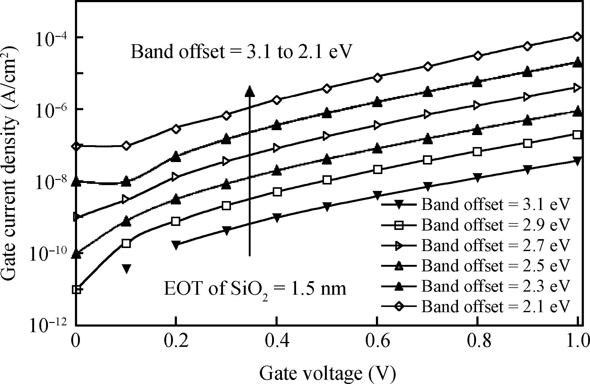
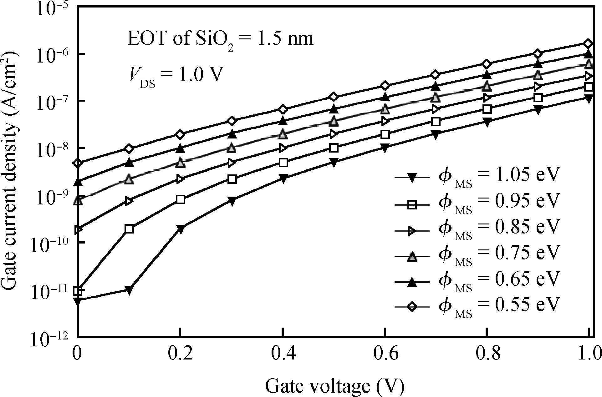
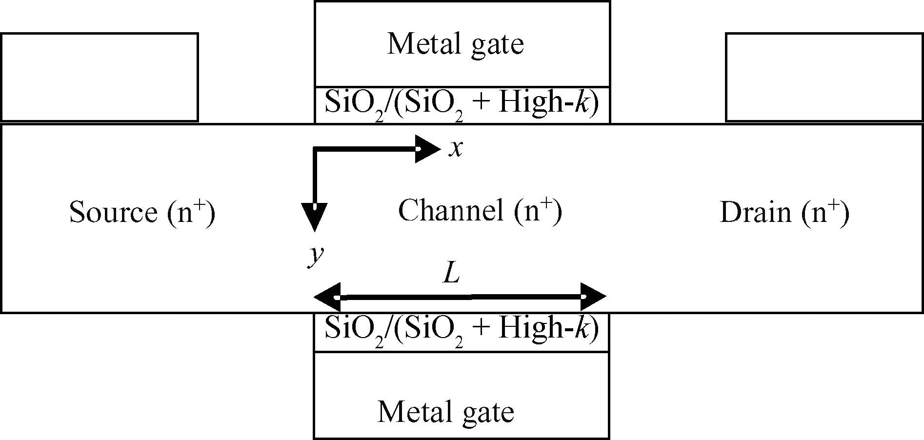
A junctionless transistor is emerging as a most promising device for the future technology in the decananometer regime. To explore and exploit the behavior completely, the understanding of gate tunneling current is of great importance. In this paper we have explored the gate tunneling current of a double gate junctionless transistor(DGJLT) for the first time through an analytical model, to meet the future requirement of expected high-
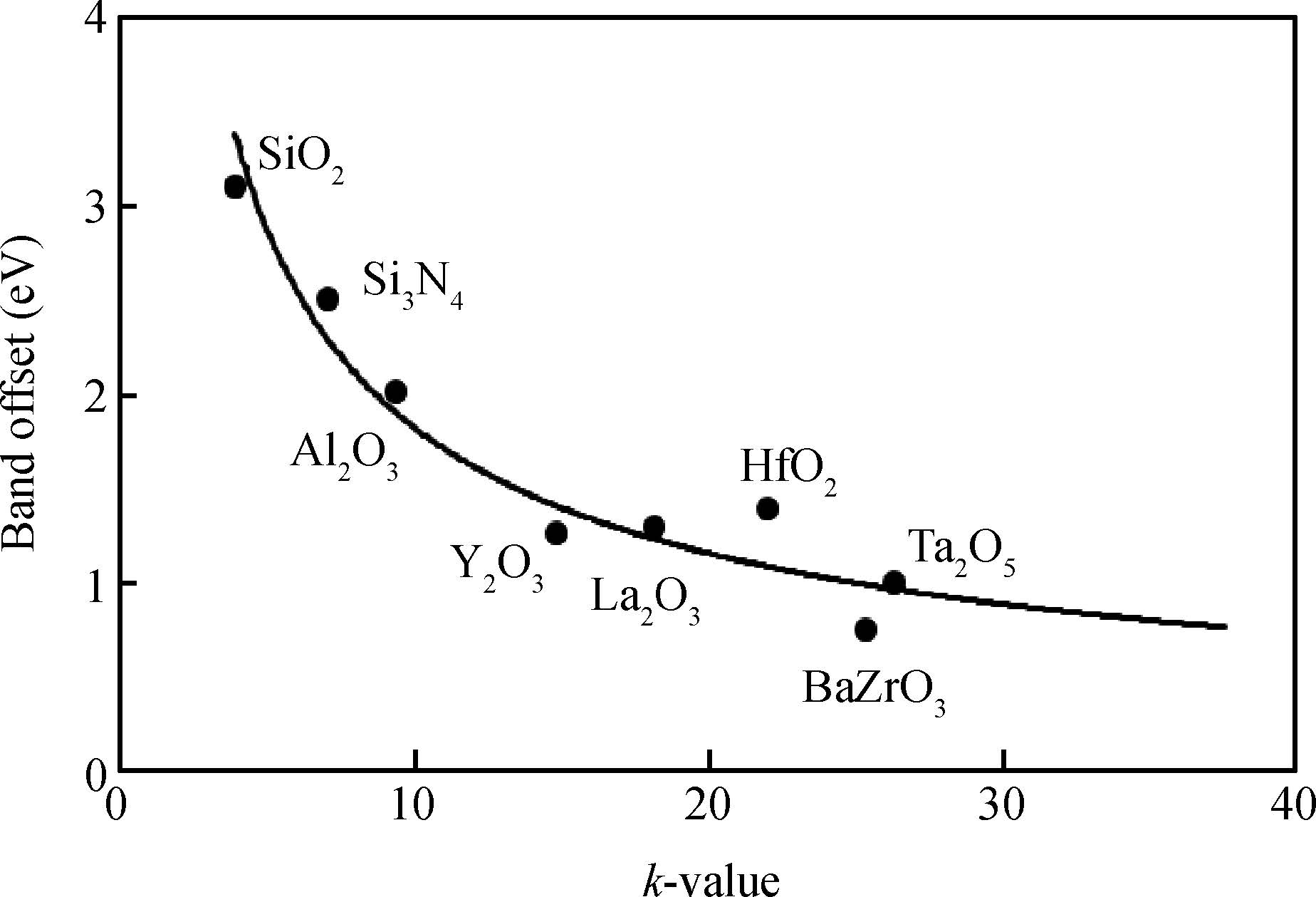
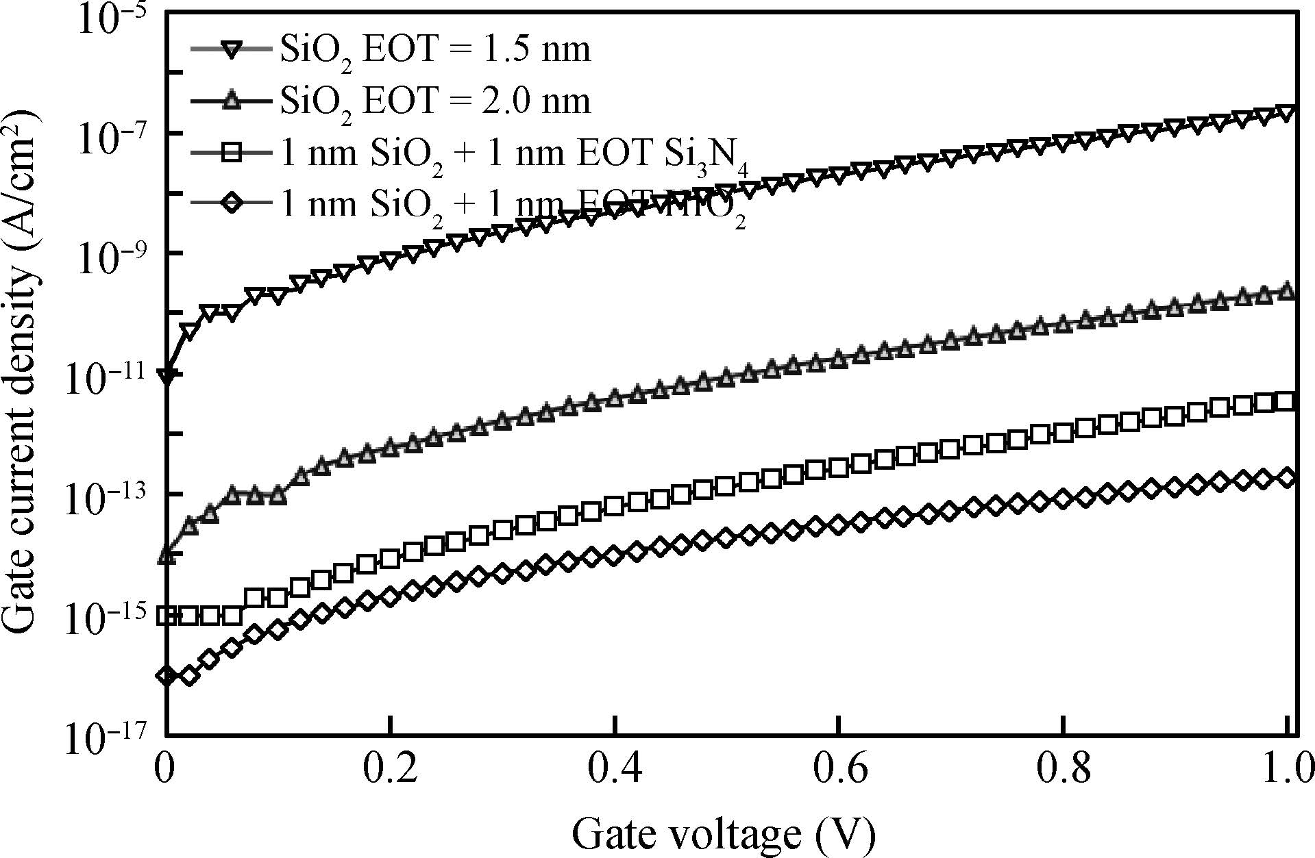
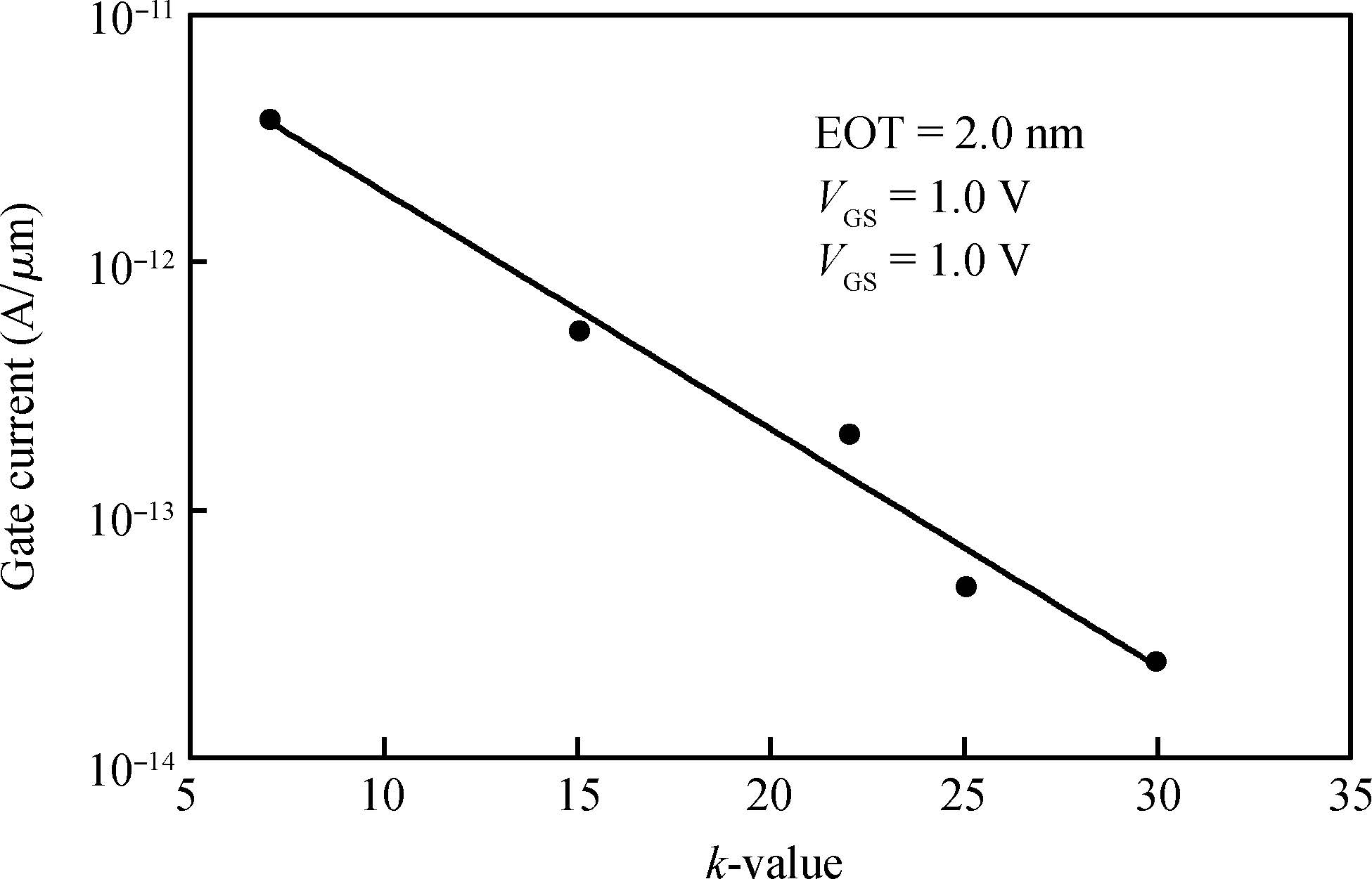
k gate dielectric material that could replace SiO
2. We therefore present the high-k gate stacked architecture of the DGJLT to minimize the gate tunneling current. This paper also demonstrates the impact of conduction band offset, workfunction difference and
k-values on the tunneling current of the DGJLT.


 DownLoad: