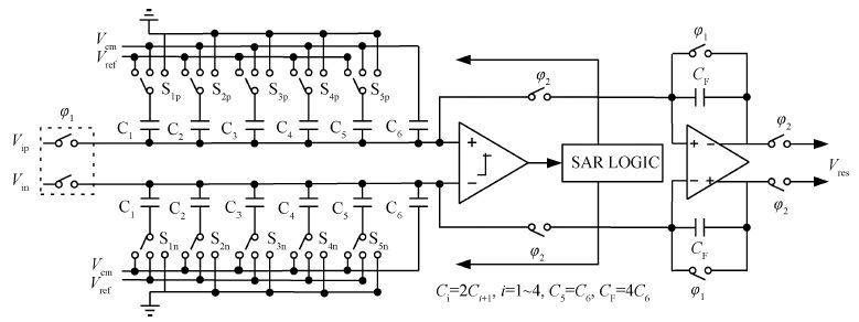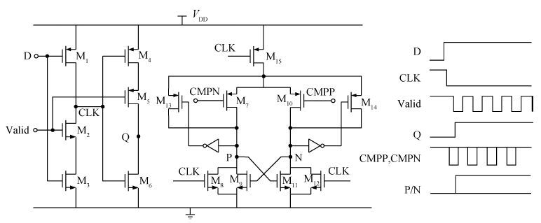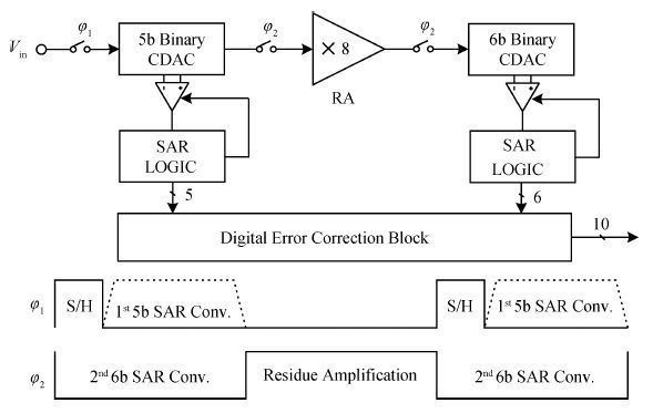
Fig. 1.
Block diagram of the proposed ADC and its timing diagram.
SEMICONDUCTOR INTEGRATED CIRCUITS
Yi Shen, Shubin Liu and Zhangming Zhu
Corresponding author: Zhangming Zhu, Email: zhangmingzhu@xidian.edu.cn
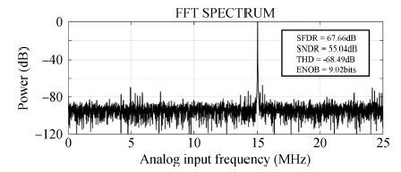
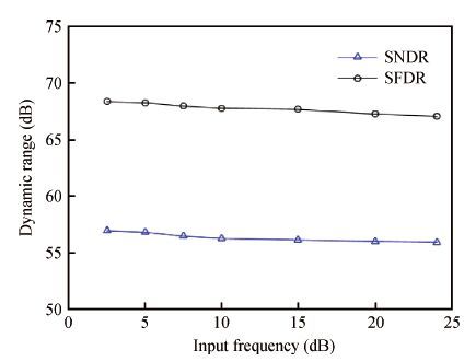
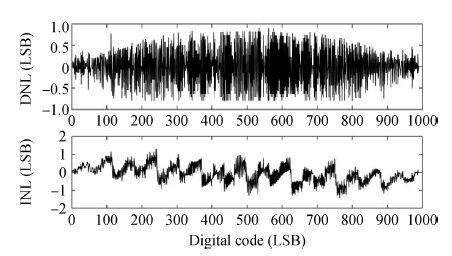
Abstract: A 10-bit 50 MS/s pipelined SAR ADC is presented which pipelines a 5-bit SAR-based MDAC with a 6-bit SAR ADC. The 1-bit redundancy relaxes the requirement for the sub-ADC decision in accuracy. The SAR-based and "half-gain" MDAC reduce the power consumption and core area. The dynamic comparator and SAR control logic are applied to reduce power consumption. Implemented in 180 nm CMOS, the fabricated ADC achieves 56.04 dB SNDR and 5mW power consumption from 1.8 V power supply at 50 MS/s.
| [1] |
Fang B N, Wu J T. A 10-Bit 300-MS/s pipelined ADC with digital calibration and digital bias generation. IEEE J Solid State Circuits, 2013, 48(3):670
|
| [2] |
Hong Hui, Li Shiliang, Zhou Tao. Design of a low power 10 bit 300 ksps multi-channel SAR ADC for wireless sensor network applications. Journal of Semiconductors, 2015, 36(4):045009
|
| [3] |
Lee C C, Flynn M P. A SAR-assisted two-stage pipeline ADC. IEEE J Solid State Circuits, 2011, 46(4):859
|
| [4] |
Furuta M, Nozawa M, Itakura T. A 10-bit, 40-MS/s, 1.21 mW pipelined SAR ADC using single-ended 1.5-bit/cycle conversion technique. IEEE J Solid-State Circuits, 2011, 46(6):1360
|
| [5] |
Zhu Y, Chan C H, Chio U F, et al. A 10-bit 100-MS/s reference-free SAR ADC in 90 nm CMOS. IEEE J Solid-State Circuits, 2010, 45(6):1111
|
| [6] |
Liu C C, Chang S J, Huang C Y, et al. A 10-bit 50-MS/s SAR ADC with a monotonic capacitor switching procedure. IEEE J Solid-State Circuits, 2010, 45(4):731
|
| [7] |
Zhu Zhangming, Xiao Yu, Xu Lifeng, et al. An 8/10 bit 200/100 MS/s configurable asynchronous SAR ADC. Analog Integrated Circuits and Signal Processing, 2013, 77(2):249
|
| [8] |
Harpe P J A, Zhou C, Yu B, et al. A 26μ W 8 bit 10 MS/s asynchronous SAR ADC for low energy radios. IEEE J Solid-State Circuits, 2011, 46(7):1585
|
| [9] |
Gong Zheng, Hu Xueqing, Yan Jun, et al. A 1.2 V dual-channel 10 bit pipeline ADC in 55 nm CMOS for WLAN receivers. Journal of Semiconductors, 2013, 34(9):095004
|
| [10] |
Qiao Ning, Zhang Guoquan, Yang Bo, et al. A 10-bit 50-MS/s reference-free low power SAR ADC in 0.18μm SOI CMOS technology. Journal of Semiconductors, 2012, 33(9):095005
|
Table 1. PERFORMANCE COMPARISON.
| Parameter | Reference [9] | Reference [10] | Reference [4] | This work |
| Technology | 55 nm | 0.18 μm | 65 nm | 0.18 μm |
| Supply (V) | 1.2 | 2.0 | 1.1 | 1.8 |
| ore area (mm2 | 0.78 | 0.26 | 0.06 | 0.16 |
| Resolution (bit) | 10 | 10 | 10 | 10 |
| Sampling rate (MHz) | 80 | 50 | 40 | 50 |
| SNDR (dB) | 56.5 | 56.8 | 55.1 | 56.04 |
| SFDR (dB) | 61.3 | 64.8 | 71.5 | 67.66 |
| Power (mW) | 19.2 | 1.72 | 1.21 | 5.0 |
| FoM (fJ/conv.-step) | 440 | 61 | 65 | 192 |
 DownLoad: CSV
| [1] |
Fang B N, Wu J T. A 10-Bit 300-MS/s pipelined ADC with digital calibration and digital bias generation. IEEE J Solid State Circuits, 2013, 48(3):670
|
| [2] |
Hong Hui, Li Shiliang, Zhou Tao. Design of a low power 10 bit 300 ksps multi-channel SAR ADC for wireless sensor network applications. Journal of Semiconductors, 2015, 36(4):045009
|
| [3] |
Lee C C, Flynn M P. A SAR-assisted two-stage pipeline ADC. IEEE J Solid State Circuits, 2011, 46(4):859
|
| [4] |
Furuta M, Nozawa M, Itakura T. A 10-bit, 40-MS/s, 1.21 mW pipelined SAR ADC using single-ended 1.5-bit/cycle conversion technique. IEEE J Solid-State Circuits, 2011, 46(6):1360
|
| [5] |
Zhu Y, Chan C H, Chio U F, et al. A 10-bit 100-MS/s reference-free SAR ADC in 90 nm CMOS. IEEE J Solid-State Circuits, 2010, 45(6):1111
|
| [6] |
Liu C C, Chang S J, Huang C Y, et al. A 10-bit 50-MS/s SAR ADC with a monotonic capacitor switching procedure. IEEE J Solid-State Circuits, 2010, 45(4):731
|
| [7] |
Zhu Zhangming, Xiao Yu, Xu Lifeng, et al. An 8/10 bit 200/100 MS/s configurable asynchronous SAR ADC. Analog Integrated Circuits and Signal Processing, 2013, 77(2):249
|
| [8] |
Harpe P J A, Zhou C, Yu B, et al. A 26μ W 8 bit 10 MS/s asynchronous SAR ADC for low energy radios. IEEE J Solid-State Circuits, 2011, 46(7):1585
|
| [9] |
Gong Zheng, Hu Xueqing, Yan Jun, et al. A 1.2 V dual-channel 10 bit pipeline ADC in 55 nm CMOS for WLAN receivers. Journal of Semiconductors, 2013, 34(9):095004
|
| [10] |
Qiao Ning, Zhang Guoquan, Yang Bo, et al. A 10-bit 50-MS/s reference-free low power SAR ADC in 0.18μm SOI CMOS technology. Journal of Semiconductors, 2012, 33(9):095005
|


Article views: 4623 Times PDF downloads: 150 Times Cited by: 0 Times
Received: 06 August 2015 Revised: 09 September 2015 Online: Published: 01 June 2016
| Citation: |
Yi Shen, Shubin Liu, Zhangming Zhu. A 10 b 50 MS/s two-stage pipelined SAR ADC in 180 nm CMOS[J]. Journal of Semiconductors, 2016, 37(6): 065001. doi: 10.1088/1674-4926/37/6/065001
****
Y Shen, S B Liu, Z M Zhu. A 10 b 50 MS/s two-stage pipelined SAR ADC in 180 nm CMOS[J]. J. Semicond., 2016, 37(6): 065001. doi: 10.1088/1674-4926/37/6/065001.

|
| [1] |
Fang B N, Wu J T. A 10-Bit 300-MS/s pipelined ADC with digital calibration and digital bias generation. IEEE J Solid State Circuits, 2013, 48(3):670
|
| [2] |
Hong Hui, Li Shiliang, Zhou Tao. Design of a low power 10 bit 300 ksps multi-channel SAR ADC for wireless sensor network applications. Journal of Semiconductors, 2015, 36(4):045009
|
| [3] |
Lee C C, Flynn M P. A SAR-assisted two-stage pipeline ADC. IEEE J Solid State Circuits, 2011, 46(4):859
|
| [4] |
Furuta M, Nozawa M, Itakura T. A 10-bit, 40-MS/s, 1.21 mW pipelined SAR ADC using single-ended 1.5-bit/cycle conversion technique. IEEE J Solid-State Circuits, 2011, 46(6):1360
|
| [5] |
Zhu Y, Chan C H, Chio U F, et al. A 10-bit 100-MS/s reference-free SAR ADC in 90 nm CMOS. IEEE J Solid-State Circuits, 2010, 45(6):1111
|
| [6] |
Liu C C, Chang S J, Huang C Y, et al. A 10-bit 50-MS/s SAR ADC with a monotonic capacitor switching procedure. IEEE J Solid-State Circuits, 2010, 45(4):731
|
| [7] |
Zhu Zhangming, Xiao Yu, Xu Lifeng, et al. An 8/10 bit 200/100 MS/s configurable asynchronous SAR ADC. Analog Integrated Circuits and Signal Processing, 2013, 77(2):249
|
| [8] |
Harpe P J A, Zhou C, Yu B, et al. A 26μ W 8 bit 10 MS/s asynchronous SAR ADC for low energy radios. IEEE J Solid-State Circuits, 2011, 46(7):1585
|
| [9] |
Gong Zheng, Hu Xueqing, Yan Jun, et al. A 1.2 V dual-channel 10 bit pipeline ADC in 55 nm CMOS for WLAN receivers. Journal of Semiconductors, 2013, 34(9):095004
|
| [10] |
Qiao Ning, Zhang Guoquan, Yang Bo, et al. A 10-bit 50-MS/s reference-free low power SAR ADC in 0.18μm SOI CMOS technology. Journal of Semiconductors, 2012, 33(9):095005
|

 WeChat ID
Journal of Semiconductors © 2017 All Rights Reserved 京ICP备05085259号-2