


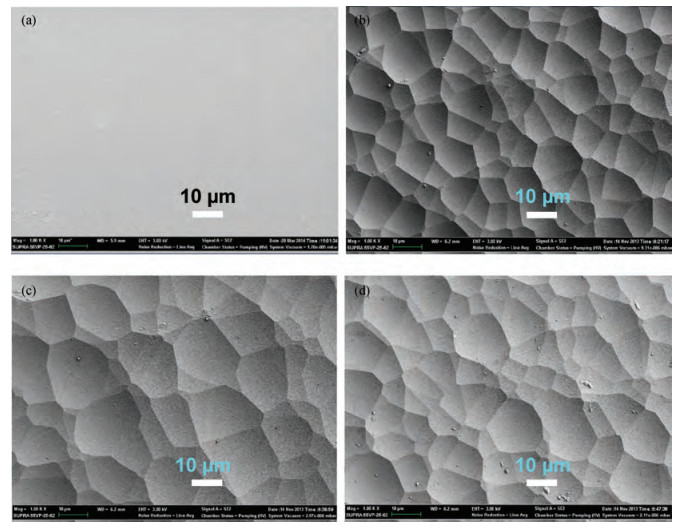
Fig. 1.
Typical SEM images of chemically etched superwhite glasses with different treatment rounds: (a) 0 (flat glass), (b) 3 R, (c) 6 R and (d) 8 R.
SEMICONDUCTOR MATERIALS
Xinliang Chen1, 2, 3, , Jieming Liu1, 2, 3, Jia Fang1, 2, 3, Ze Chen1, 2, 3, Ying Zhao1, 2, 3 and Xiaodan Zhang1, 2, 3
Corresponding author: Chen Xinliang, Email: cxlruzhou@163.com
Abstract: Textured glass substrates with crater-like feature sizes of 5-30μm were obtained using the chemical etching method through adjusting the treatment round (R). Pyramid-like boron-doped zinc oxide (ZnO:B) films with feature sizes of 300-800 nm were deposited on the etched glass substrates by the metal organic chemical deposition (MOCVD) technique using water, diethylzinc and 1%-hydrogen-diluted diborane. The ZnO:B films on the etched glass with micro/nano double textures presented a much stronger light-scattering capability than the conventional ZnO:B on the flat glass and their electrical properties changed little. Typical etched glass-3R/ZnO:B exhibited a high root mean square (RMS) roughness of 160 nm. The haze values at the wavelengths of 550 nm and 850 nm for etched glass-3R/ZnO:B sample were 61% and 42%, respectively. Finally, the optimized etched glass/ZnO:B was applied in the silicon (Si) based thin film solar cells. The high haze etched glass/ZnO:B substrates have potential merits for thin film solar cells.
Keywords: semiconductors, surfaces, thin films, crystal growth, optical properties
| [1] |
Shah A V, Schade H, Vanecek M, et al. Thin-film silicon solar cell technology. Progress in Photovoltaics: Research and Applications, 2004, 12: 113 doi: 10.1002/(ISSN)1099-159X
|
| [2] |
Terakawa A. Review of thin-film silicon deposition techniques for high-efficiency solar cells developed at Panasonic/Sanyo. Solar Energy Materials and Solar Cells, 2013, 119: 204 doi: 10.1016/j.solmat.2013.06.044
|
| [3] |
Kim S, Chung J W, Lee H, et al. Remarkable progress in thin-film silicon solar cells using high-efficiency triple-junction technology. Solar Energy Materials and Solar Cells, 2013, 119: 26 doi: 10.1016/j.solmat.2013.04.016
|
| [4] |
Muller J, Rech B, Springer J, et al. TCO and light trapping in silicon thin film solar cells. Solar Energy, 2004, 77: 917 doi: 10.1016/j.solener.2004.03.015
|
| [5] |
Chen X L, Xu B H, Xue J M, et al. Boron-doped zinc oxide thin films for large-area solar cells grown by metal organic chemical vapor deposition. Thin Solid Films, 2007, 515: 3753 doi: 10.1016/j.tsf.2006.09.039
|
| [6] |
Üpping J, Bielawny A, Wehrspohn R B, et al. Three-dimensional photonic crystal intermediate reflectors for enhanced light-trapping in tandem solar cells. Advanced Materials, 2011, 23: 3896 doi: 10.1002/adma.v23.34
|
| [7] |
Feltrin A, Meguro T, Van Assche E, et al. Advanced light trapping designs for high efficiency thin film silicon solar cells. Solar Energy Materials and Solar Cells, 2013, 119: 219 doi: 10.1016/j.solmat.2013.07.012
|
| [8] |
Mahadik M A, Hunge Y M, Shinde S S, et al. Semiconducting properties of aluminum-doped ZnO thin films grown by spray pyrolysis technique. Journal of Semiconductors, 2015, 36(3): 033002 doi: 10.1088/1674-4926/36/3/033002
|
| [9] |
Saha S K, Rahman M A, Sarkar M R H, et al. Effect of Co doping on structural, optical, electrical and thermal properties of nanostructured ZnO thin films. Journal of Semiconductors, 2015, 36(3): 033004 doi: 10.1088/1674-4926/36/3/033004
|
| [10] |
Karim A M M T, Khan M K R, Rahman M M. Structural and opto-electrical properties of pyrolized ZnO-CdO crystalline thin films. Journal of Semiconductors, 2015, 36(5): 053001 doi: 10.1088/1674-4926/36/5/053001
|
| [11] |
Liu Yang, Ma Jianping, Liu Fuli, et al. Physical vapor transport crystal growth of ZnO. Journal of Semiconductors, 2014, 35(3): 033001 doi: 10.1088/1674-4926/35/3/033001
|
| [12] |
Fay S, Feitknecht L, Schlüchter R, et al. Rough ZnO layers by LP-CVD process and their effect in improving performances of amorphous and microcrystalline silicon solar cells. Solar Energy Materials and Solar Cells, 2006, 90: 2960 doi: 10.1016/j.solmat.2006.06.003
|
| [13] |
Berginski M, Hüpkes J, Schulte M, et al. The effect of front ZnO:Al surface texture and optical transparency on efficient light trapping in silicon thin-film solar cells. J Appl Phys 2007, 101: 074903 doi: 10.1063/1.2715554
|
| [14] |
Chen X L, Li L N, Wang F, et al. Natively textured surface aluminum-doped zinc oxide transparent conductive layers for thin film solar cells via pulsed direct-current reactive magnetron sputtering. Thin Solid Films, 2012, 520: 5392 doi: 10.1016/j.tsf.2012.03.120
|
| [15] |
Steinhauser J, Boucher J F, Omnes E, et al. Improving low pressure chemical vapor deposited zinc oxide contacts for thin film silicon solar cells by using rough glass substrates. Thin Solid Films, 2011, 520: 1218 doi: 10.1016/j.tsf.2011.06.080
|
| [16] |
Kim J, Battaglia C, Charriére M, et al. 9.4% efficient amorphous silicon solar cell on high aspect-ratio glass microcones. Advanced Materials, 2014, 26: 4082 doi: 10.1002/adma.v26.24
|
| [17] |
Addonizio M L, Antonaia A. Surface morphology and light scattering properties of plasma etched ZnO:B films grown by LP-MOCVD for silicon thin film solar cells. Thin Solid Films, 2009, 518: 1026 doi: 10.1016/j.tsf.2009.07.200
|
| [18] |
Boccard M, Battaglia C, Hanni S, et al. Multiscale transparent electrode architecture for efficient light management and carrier collection in solar cells. Nano Lett, 2012, 12: 1344 doi: 10.1021/nl203909u
|
| [19] |
Hongsingthong A, Krajangsang T, Yunaz I A, et al. ZnO films with very high haze value for use as front transparent conductive oxide films in thin-film silicon solar cells. Applied Physics Express, 2010, 3: 051102 doi: 10.1143/APEX.3.051102
|
| [20] |
Hongsingthong A, Krajangsang T, Limmanee A, et al. Development of textured ZnO-coated low-cost glass substrate with very high haze ratio for silicon-based thin film solar cells. Thin Solid Films, 2013, 537: 291 doi: 10.1016/j.tsf.2013.04.138
|
| [21] |
Janthong B, Moriya Y, Hongsingthong A, et al. Management of light-trapping effect for a-Si:H/μc-Si:H tandem solar cells using novel substrates, based on MOCVD ZnO and etched white glass. Solar Energy Materials and Solar Cells, 2013, 119: 209 doi: 10.1016/j.solmat.2013.06.045
|
| [22] |
Chen X L, Geng X H, Xue J M, et al. Temperature-dependent growth of zinc oxide thin films grown by metal organic chemical vapor deposition. J Cryst Growth, 2006, 296: 43 doi: 10.1016/j.jcrysgro.2006.08.028
|
| [23] |
Tan H, Psomadaki E, Isabella O, et al. Micro-textures for efficient light trapping and improved electrical performance in thin-film nanocrystalline silicon solar cells. Appl Phys Lett, 2013, 103: 173905 doi: 10.1063/1.4826639
|
| [24] |
Chen X L, Yan C B, Chen X, et al. Textured surface ZnO:B and IWO/ZnO:B TCO layers for Si-based thin film solar cells. Proceeding of the 26th European Photovoltaic Solar Energy Conference (EU-PVSEC), Hamburg, Germany, 2011: 2482 http://cn.bing.com/academic/profile?id=69555615&encoded=0&v=paper_preview&mkt=zh-cn
|
| [25] |
Krc J, Smole F, Topic M, Analysis of light scattering in amorphous Si:H solar cells by a one-dimensional semi-coherent optical model. Progress in Photovoltaics: Research and Application 2013, 11: 15 http://cn.bing.com/academic/profile?id=2069741452&encoded=0&v=paper_preview&mkt=zh-cn
|
| [26] |
Steinhauser J, Faÿ S, Oliveira N, et al. Transition between grain boundary and intragrain scattering transport mechanisms in boron-doped zinc oxide thin films. Appl Phys Lett, 2007, 90: 142107 doi: 10.1063/1.2719158
|
| [27] |
Shah A. Thin-film silicon solar cells. Lausanne: Swiss EPFL Press, 2010
|
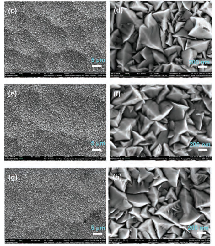
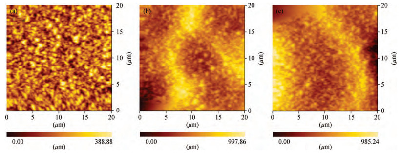

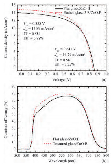
Table 1. Electrical properties of ZnO:B fims on chemically etched superwhite glasses with different treatment rounds.
 |
| [1] |
Shah A V, Schade H, Vanecek M, et al. Thin-film silicon solar cell technology. Progress in Photovoltaics: Research and Applications, 2004, 12: 113 doi: 10.1002/(ISSN)1099-159X
|
| [2] |
Terakawa A. Review of thin-film silicon deposition techniques for high-efficiency solar cells developed at Panasonic/Sanyo. Solar Energy Materials and Solar Cells, 2013, 119: 204 doi: 10.1016/j.solmat.2013.06.044
|
| [3] |
Kim S, Chung J W, Lee H, et al. Remarkable progress in thin-film silicon solar cells using high-efficiency triple-junction technology. Solar Energy Materials and Solar Cells, 2013, 119: 26 doi: 10.1016/j.solmat.2013.04.016
|
| [4] |
Muller J, Rech B, Springer J, et al. TCO and light trapping in silicon thin film solar cells. Solar Energy, 2004, 77: 917 doi: 10.1016/j.solener.2004.03.015
|
| [5] |
Chen X L, Xu B H, Xue J M, et al. Boron-doped zinc oxide thin films for large-area solar cells grown by metal organic chemical vapor deposition. Thin Solid Films, 2007, 515: 3753 doi: 10.1016/j.tsf.2006.09.039
|
| [6] |
Üpping J, Bielawny A, Wehrspohn R B, et al. Three-dimensional photonic crystal intermediate reflectors for enhanced light-trapping in tandem solar cells. Advanced Materials, 2011, 23: 3896 doi: 10.1002/adma.v23.34
|
| [7] |
Feltrin A, Meguro T, Van Assche E, et al. Advanced light trapping designs for high efficiency thin film silicon solar cells. Solar Energy Materials and Solar Cells, 2013, 119: 219 doi: 10.1016/j.solmat.2013.07.012
|
| [8] |
Mahadik M A, Hunge Y M, Shinde S S, et al. Semiconducting properties of aluminum-doped ZnO thin films grown by spray pyrolysis technique. Journal of Semiconductors, 2015, 36(3): 033002 doi: 10.1088/1674-4926/36/3/033002
|
| [9] |
Saha S K, Rahman M A, Sarkar M R H, et al. Effect of Co doping on structural, optical, electrical and thermal properties of nanostructured ZnO thin films. Journal of Semiconductors, 2015, 36(3): 033004 doi: 10.1088/1674-4926/36/3/033004
|
| [10] |
Karim A M M T, Khan M K R, Rahman M M. Structural and opto-electrical properties of pyrolized ZnO-CdO crystalline thin films. Journal of Semiconductors, 2015, 36(5): 053001 doi: 10.1088/1674-4926/36/5/053001
|
| [11] |
Liu Yang, Ma Jianping, Liu Fuli, et al. Physical vapor transport crystal growth of ZnO. Journal of Semiconductors, 2014, 35(3): 033001 doi: 10.1088/1674-4926/35/3/033001
|
| [12] |
Fay S, Feitknecht L, Schlüchter R, et al. Rough ZnO layers by LP-CVD process and their effect in improving performances of amorphous and microcrystalline silicon solar cells. Solar Energy Materials and Solar Cells, 2006, 90: 2960 doi: 10.1016/j.solmat.2006.06.003
|
| [13] |
Berginski M, Hüpkes J, Schulte M, et al. The effect of front ZnO:Al surface texture and optical transparency on efficient light trapping in silicon thin-film solar cells. J Appl Phys 2007, 101: 074903 doi: 10.1063/1.2715554
|
| [14] |
Chen X L, Li L N, Wang F, et al. Natively textured surface aluminum-doped zinc oxide transparent conductive layers for thin film solar cells via pulsed direct-current reactive magnetron sputtering. Thin Solid Films, 2012, 520: 5392 doi: 10.1016/j.tsf.2012.03.120
|
| [15] |
Steinhauser J, Boucher J F, Omnes E, et al. Improving low pressure chemical vapor deposited zinc oxide contacts for thin film silicon solar cells by using rough glass substrates. Thin Solid Films, 2011, 520: 1218 doi: 10.1016/j.tsf.2011.06.080
|
| [16] |
Kim J, Battaglia C, Charriére M, et al. 9.4% efficient amorphous silicon solar cell on high aspect-ratio glass microcones. Advanced Materials, 2014, 26: 4082 doi: 10.1002/adma.v26.24
|
| [17] |
Addonizio M L, Antonaia A. Surface morphology and light scattering properties of plasma etched ZnO:B films grown by LP-MOCVD for silicon thin film solar cells. Thin Solid Films, 2009, 518: 1026 doi: 10.1016/j.tsf.2009.07.200
|
| [18] |
Boccard M, Battaglia C, Hanni S, et al. Multiscale transparent electrode architecture for efficient light management and carrier collection in solar cells. Nano Lett, 2012, 12: 1344 doi: 10.1021/nl203909u
|
| [19] |
Hongsingthong A, Krajangsang T, Yunaz I A, et al. ZnO films with very high haze value for use as front transparent conductive oxide films in thin-film silicon solar cells. Applied Physics Express, 2010, 3: 051102 doi: 10.1143/APEX.3.051102
|
| [20] |
Hongsingthong A, Krajangsang T, Limmanee A, et al. Development of textured ZnO-coated low-cost glass substrate with very high haze ratio for silicon-based thin film solar cells. Thin Solid Films, 2013, 537: 291 doi: 10.1016/j.tsf.2013.04.138
|
| [21] |
Janthong B, Moriya Y, Hongsingthong A, et al. Management of light-trapping effect for a-Si:H/μc-Si:H tandem solar cells using novel substrates, based on MOCVD ZnO and etched white glass. Solar Energy Materials and Solar Cells, 2013, 119: 209 doi: 10.1016/j.solmat.2013.06.045
|
| [22] |
Chen X L, Geng X H, Xue J M, et al. Temperature-dependent growth of zinc oxide thin films grown by metal organic chemical vapor deposition. J Cryst Growth, 2006, 296: 43 doi: 10.1016/j.jcrysgro.2006.08.028
|
| [23] |
Tan H, Psomadaki E, Isabella O, et al. Micro-textures for efficient light trapping and improved electrical performance in thin-film nanocrystalline silicon solar cells. Appl Phys Lett, 2013, 103: 173905 doi: 10.1063/1.4826639
|
| [24] |
Chen X L, Yan C B, Chen X, et al. Textured surface ZnO:B and IWO/ZnO:B TCO layers for Si-based thin film solar cells. Proceeding of the 26th European Photovoltaic Solar Energy Conference (EU-PVSEC), Hamburg, Germany, 2011: 2482 http://cn.bing.com/academic/profile?id=69555615&encoded=0&v=paper_preview&mkt=zh-cn
|
| [25] |
Krc J, Smole F, Topic M, Analysis of light scattering in amorphous Si:H solar cells by a one-dimensional semi-coherent optical model. Progress in Photovoltaics: Research and Application 2013, 11: 15 http://cn.bing.com/academic/profile?id=2069741452&encoded=0&v=paper_preview&mkt=zh-cn
|
| [26] |
Steinhauser J, Faÿ S, Oliveira N, et al. Transition between grain boundary and intragrain scattering transport mechanisms in boron-doped zinc oxide thin films. Appl Phys Lett, 2007, 90: 142107 doi: 10.1063/1.2719158
|
| [27] |
Shah A. Thin-film silicon solar cells. Lausanne: Swiss EPFL Press, 2010
|


Article views: 3481 Times PDF downloads: 22 Times Cited by: 0 Times
Received: 05 December 2015 Revised: 12 January 2016 Online: Published: 01 August 2016
| Citation: |
Xinliang Chen, Jieming Liu, Jia Fang, Ze Chen, Ying Zhao, Xiaodan Zhang. High haze textured surface B-doped ZnO-TCO films on wet-chemically etched glass substrates for thin film solar cells[J]. Journal of Semiconductors, 2016, 37(8): 083003. doi: 10.1088/1674-4926/37/8/083003
****
X L Chen, J M Liu, J Fang, Z Chen, Y Zhao, X D Zhang. High haze textured surface B-doped ZnO-TCO films on wet-chemically etched glass substrates for thin film solar cells[J]. J. Semicond., 2016, 37(8): 083003. doi: 10.1088/1674-4926/37/8/083003.

|
| [1] |
Shah A V, Schade H, Vanecek M, et al. Thin-film silicon solar cell technology. Progress in Photovoltaics: Research and Applications, 2004, 12: 113 doi: 10.1002/(ISSN)1099-159X
|
| [2] |
Terakawa A. Review of thin-film silicon deposition techniques for high-efficiency solar cells developed at Panasonic/Sanyo. Solar Energy Materials and Solar Cells, 2013, 119: 204 doi: 10.1016/j.solmat.2013.06.044
|
| [3] |
Kim S, Chung J W, Lee H, et al. Remarkable progress in thin-film silicon solar cells using high-efficiency triple-junction technology. Solar Energy Materials and Solar Cells, 2013, 119: 26 doi: 10.1016/j.solmat.2013.04.016
|
| [4] |
Muller J, Rech B, Springer J, et al. TCO and light trapping in silicon thin film solar cells. Solar Energy, 2004, 77: 917 doi: 10.1016/j.solener.2004.03.015
|
| [5] |
Chen X L, Xu B H, Xue J M, et al. Boron-doped zinc oxide thin films for large-area solar cells grown by metal organic chemical vapor deposition. Thin Solid Films, 2007, 515: 3753 doi: 10.1016/j.tsf.2006.09.039
|
| [6] |
Üpping J, Bielawny A, Wehrspohn R B, et al. Three-dimensional photonic crystal intermediate reflectors for enhanced light-trapping in tandem solar cells. Advanced Materials, 2011, 23: 3896 doi: 10.1002/adma.v23.34
|
| [7] |
Feltrin A, Meguro T, Van Assche E, et al. Advanced light trapping designs for high efficiency thin film silicon solar cells. Solar Energy Materials and Solar Cells, 2013, 119: 219 doi: 10.1016/j.solmat.2013.07.012
|
| [8] |
Mahadik M A, Hunge Y M, Shinde S S, et al. Semiconducting properties of aluminum-doped ZnO thin films grown by spray pyrolysis technique. Journal of Semiconductors, 2015, 36(3): 033002 doi: 10.1088/1674-4926/36/3/033002
|
| [9] |
Saha S K, Rahman M A, Sarkar M R H, et al. Effect of Co doping on structural, optical, electrical and thermal properties of nanostructured ZnO thin films. Journal of Semiconductors, 2015, 36(3): 033004 doi: 10.1088/1674-4926/36/3/033004
|
| [10] |
Karim A M M T, Khan M K R, Rahman M M. Structural and opto-electrical properties of pyrolized ZnO-CdO crystalline thin films. Journal of Semiconductors, 2015, 36(5): 053001 doi: 10.1088/1674-4926/36/5/053001
|
| [11] |
Liu Yang, Ma Jianping, Liu Fuli, et al. Physical vapor transport crystal growth of ZnO. Journal of Semiconductors, 2014, 35(3): 033001 doi: 10.1088/1674-4926/35/3/033001
|
| [12] |
Fay S, Feitknecht L, Schlüchter R, et al. Rough ZnO layers by LP-CVD process and their effect in improving performances of amorphous and microcrystalline silicon solar cells. Solar Energy Materials and Solar Cells, 2006, 90: 2960 doi: 10.1016/j.solmat.2006.06.003
|
| [13] |
Berginski M, Hüpkes J, Schulte M, et al. The effect of front ZnO:Al surface texture and optical transparency on efficient light trapping in silicon thin-film solar cells. J Appl Phys 2007, 101: 074903 doi: 10.1063/1.2715554
|
| [14] |
Chen X L, Li L N, Wang F, et al. Natively textured surface aluminum-doped zinc oxide transparent conductive layers for thin film solar cells via pulsed direct-current reactive magnetron sputtering. Thin Solid Films, 2012, 520: 5392 doi: 10.1016/j.tsf.2012.03.120
|
| [15] |
Steinhauser J, Boucher J F, Omnes E, et al. Improving low pressure chemical vapor deposited zinc oxide contacts for thin film silicon solar cells by using rough glass substrates. Thin Solid Films, 2011, 520: 1218 doi: 10.1016/j.tsf.2011.06.080
|
| [16] |
Kim J, Battaglia C, Charriére M, et al. 9.4% efficient amorphous silicon solar cell on high aspect-ratio glass microcones. Advanced Materials, 2014, 26: 4082 doi: 10.1002/adma.v26.24
|
| [17] |
Addonizio M L, Antonaia A. Surface morphology and light scattering properties of plasma etched ZnO:B films grown by LP-MOCVD for silicon thin film solar cells. Thin Solid Films, 2009, 518: 1026 doi: 10.1016/j.tsf.2009.07.200
|
| [18] |
Boccard M, Battaglia C, Hanni S, et al. Multiscale transparent electrode architecture for efficient light management and carrier collection in solar cells. Nano Lett, 2012, 12: 1344 doi: 10.1021/nl203909u
|
| [19] |
Hongsingthong A, Krajangsang T, Yunaz I A, et al. ZnO films with very high haze value for use as front transparent conductive oxide films in thin-film silicon solar cells. Applied Physics Express, 2010, 3: 051102 doi: 10.1143/APEX.3.051102
|
| [20] |
Hongsingthong A, Krajangsang T, Limmanee A, et al. Development of textured ZnO-coated low-cost glass substrate with very high haze ratio for silicon-based thin film solar cells. Thin Solid Films, 2013, 537: 291 doi: 10.1016/j.tsf.2013.04.138
|
| [21] |
Janthong B, Moriya Y, Hongsingthong A, et al. Management of light-trapping effect for a-Si:H/μc-Si:H tandem solar cells using novel substrates, based on MOCVD ZnO and etched white glass. Solar Energy Materials and Solar Cells, 2013, 119: 209 doi: 10.1016/j.solmat.2013.06.045
|
| [22] |
Chen X L, Geng X H, Xue J M, et al. Temperature-dependent growth of zinc oxide thin films grown by metal organic chemical vapor deposition. J Cryst Growth, 2006, 296: 43 doi: 10.1016/j.jcrysgro.2006.08.028
|
| [23] |
Tan H, Psomadaki E, Isabella O, et al. Micro-textures for efficient light trapping and improved electrical performance in thin-film nanocrystalline silicon solar cells. Appl Phys Lett, 2013, 103: 173905 doi: 10.1063/1.4826639
|
| [24] |
Chen X L, Yan C B, Chen X, et al. Textured surface ZnO:B and IWO/ZnO:B TCO layers for Si-based thin film solar cells. Proceeding of the 26th European Photovoltaic Solar Energy Conference (EU-PVSEC), Hamburg, Germany, 2011: 2482 http://cn.bing.com/academic/profile?id=69555615&encoded=0&v=paper_preview&mkt=zh-cn
|
| [25] |
Krc J, Smole F, Topic M, Analysis of light scattering in amorphous Si:H solar cells by a one-dimensional semi-coherent optical model. Progress in Photovoltaics: Research and Application 2013, 11: 15 http://cn.bing.com/academic/profile?id=2069741452&encoded=0&v=paper_preview&mkt=zh-cn
|
| [26] |
Steinhauser J, Faÿ S, Oliveira N, et al. Transition between grain boundary and intragrain scattering transport mechanisms in boron-doped zinc oxide thin films. Appl Phys Lett, 2007, 90: 142107 doi: 10.1063/1.2719158
|
| [27] |
Shah A. Thin-film silicon solar cells. Lausanne: Swiss EPFL Press, 2010
|

 WeChat ID
Journal of Semiconductors © 2017 All Rights Reserved 京ICP备05085259号-2

 DownLoad:

