


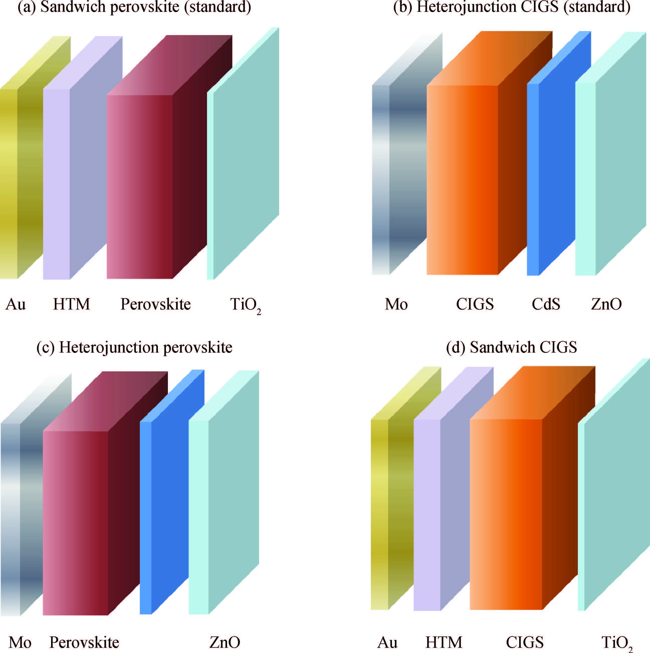
Fig. 1.
(Color online) Schematic device structures.
SPECIAL TOPIC ON PEROVSKITE SOLAR CELLS
Tianyue Wang1, Jiewei Chen1, Gaoxiang Wu1, Dandan Song1 and Meicheng Li1, 2,
Corresponding author: Meicheng Li,Email:mcli@ncepu.edu.cn
Abstract: Heterojunction and sandwich architectures are two new-type structures with great potential for solar cells. Specifically, the heterojunction structure possesses the advantages of efficient charge separation but suffers from band offset and large interface recombination; the sandwich configuration is favorable for transferring carriers but requires complex fabrication process. Here, we have designed two thin-film polycrystalline solar cells with novel structures:sandwich CIGS and heterojunction perovskite, referring to the advantages of the architectures of sandwich perovskite (standard) and heterojunction CIGS (standard) solar cells, respectively. A reliable simulation software wxAMPS is used to investigate their inherent characteristics with variation of the thickness and doping density of absorber layer. The results reveal that sandwich CIGS solar cell is able to exhibit an optimized efficiency of 20.7%, which is much higher than the standard heterojunction CIGS structure (18.48%). The heterojunction perovskite solar cell can be more efficient employing thick and doped perovskite films (16.9%) than these typically utilizing thin and weak-doping/intrinsic perovskite films (9.6%). This concept of structure modulation proves to be useful and can be applicable for other solar cells.
Keywords: sandwich CIGS solar cell, heterojunction perovskite solar cell, simulation, wxAMPS
| [1] |
Sandberg O J, Sundqvist A, Nyman M, et al. Relating charge transport, contact properties, and recombination to open-circuit voltage in sandwich-type thin-film solar cells. Phys Rev Appl, 2016, 5(4): 044005 doi: 10.1103/PhysRevApplied.5.044005
|
| [2] |
Yang Y, Chen W, Dou L T, et al. High-performance multiple-donor bulk heterojunction solar cells. Nat Photonics, 2015, 9(3): 190 doi: 10.1038/nphoton.2015.9
|
| [3] |
Wu Y M, Yang R X, Tian H M, et al. Photoelectric characteristics of CH3NH3PbI3/p-Si heterojunction. J Semicond, 2016, 37(5): 053002 doi: 10.1088/1674-4926/37/5/053002
|
| [4] |
Jin H H, Han H J, Lee M H, et al. Stable semi-transparent CH3NH3PbI3 planar sandwich solar cells. Energy Environ Sci, 2015, 8(10): 2922 doi: 10.1039/C5EE01050K
|
| [5] |
Wu W Q, Lei BX, Rao H S, et al. Hydrothermal fabrication of hierarchically anatase TiO2 nanowire arrays on FTO glass for dye-sensitized solar cells. Sci Rep, 2013, 3(2): 1352 https://www.researchgate.net/publication/235740345_Hydrothermal_Fabrication_of_Hierarchically_Anatase_TiO2_Nanowire_arrays_on_FTO_Glass_for_Dye-sensitized_Solar_Cells
|
| [6] |
Sim H, Lee J, Cho S, et al. A study on the band structure of ZnO/CdS heterojunction for CIGS solar-cell application. J Semicond Technol Sci, 2015, 15(2): 267 doi: 10.5573/JSTS.2015.15.2.267
|
| [7] |
Contreras M A, Nakada T, Hongo M, et al. ZnO/ZnS(O,OH)/Cu(In,Ga)Se2 Mo solar cell with 18.6% efficiency. Proceedings of World Conference on Photovoltaic Energy Conversion, 2003
|
| [8] |
Goetzberger A, Knobloch J, Voβ B, et al. The physics of solar cells. Imperial College Press, 2003: 384 http://cn.bing.com/academic/profile?id=eb0c728b296ec4a88349c72e297563fd&encoded=0&v=paper_preview&mkt=zh-cn
|
| [9] |
Minemoto T, Matsui T, Takakura H, et al. Theoretical analysis of the effect of conduction band offset of window/CIS layers on performance of CIS solar cells using device simulation. Sol Energy Materi Sol Cells, 2001, 67(1-4): 83 doi: 10.1016/S0927-0248(00)00266-X
|
| [10] | |
| [11] |
Nie W, Tsai H, Asadpour R, et al. High-efficiency solution-processed perovskite solar cells with millimeter-scale grains. Science, 2015, 347(6221): 522 doi: 10.1126/science.aaa0472
|
| [12] |
Wei D, Wang T Y, Ji J, et al. Photo-induced degradation of lead halide perovskite solar cells caused by the hole transport layer/metal electrode interface. J Mater Chem A, 2016, 4(5): 1991 doi: 10.1039/C5TA08622A
|
| [13] |
Chen W Z, Huang X, Cheng Q J, et al. Simulation analysis of heterojunction ZnO/CdS/Cu(In,Ga)Se2 thin-film solar cells using wxAMPS. Optik-Int J Light Electron Opt, 2015, 127: 182 https://www.researchgate.net/publication/284001321_Simulation_analysis_of_heterojunction_ZnOCdSCuInGaSe2_thin-film_solar_cells_using_wxAMPS
|
| [14] |
Liu Y M, Sun Y, Rockett A. A new simulation software of solar cells-wxAMPS. Sol Energy Mater Sol Cells, 2012, 98(1): 124 http://cn.bing.com/academic/profile?id=8c0d5d842344d77f2958ac4a37c24c82&encoded=0&v=paper_preview&mkt=zh-cn
|
| [15] |
Song D D, Wei D, Cui P, et al. Dual function interfacial layer for highly efficient and stable lead halide perovskite solar cells. J Mater Chem A, 2016, 4(16): 6091 doi: 10.1039/C6TA00577B
|
| [16] | |
| [17] |
De Wolf S, Holovsky J, Moon S J, et al. Organometallic halide perovskites: sharp optical absorption edge and its relation to photovoltaic performance. J Phys Chem Lett, 2014, 5(6): 1035 doi: 10.1021/jz500279b
|
| [18] |
Wojciechowski K, Saliba M, Leijtens T, et al. Sub-150℃ processed meso-superstructured perovskite solar cells with enhanced efficiency. Energy Environ Sci, 2014, 7(3): 1142 doi: 10.1039/C3EE43707H
|
| [19] |
Liu W Q, Zhang Y. Electrical characterization of TiO2/CH3 NH3PbI3 heterojunction solar cells. J Mater Chem A, 2014, 2(26): 10244 doi: 10.1039/c4ta01219d
|
| [20] |
Snaith H J, Gräzel M. Electron and hole transport through mesoporous TiO2 infiltrated with spiro-MeOTAD. Adv Mater, 2007, 19(21): 3643 doi: 10.1002/(ISSN)1521-4095
|
| [21] |
Noh J H, Sang H I, Jin H H, et al. Chemical management for colorful, efficient, and stable inorganic-organic hybrid nanostructured solar cells. Nano Lett, 2013, 13(4): 1764 doi: 10.1021/nl400349b
|
| [22] |
Laban W A, Etgar L. Depleted hole conductor-free lead halide iodide heterojunction solar cells. Energy Environ Sci, 2013, 6(11): 3249 doi: 10.1039/c3ee42282h
|
| [23] |
Stoumpos C C, Malliakas C D, Kanatzidis M G. Semiconducting tin and lead iodide perovskites with organic cations: phase transitions, high mobilities, and near-infrared photoluminescent properties. Inorg Chem, 2013, 52(15): 9019 doi: 10.1021/ic401215x
|
| [24] |
Fonash S J. Solar cell device physics. 2nd Ed. 2010
|
| [25] |
Liu Y M. Modeling of Cu(In,Ga)Se2 thin film solar cell device. Nankai University, 2012
|
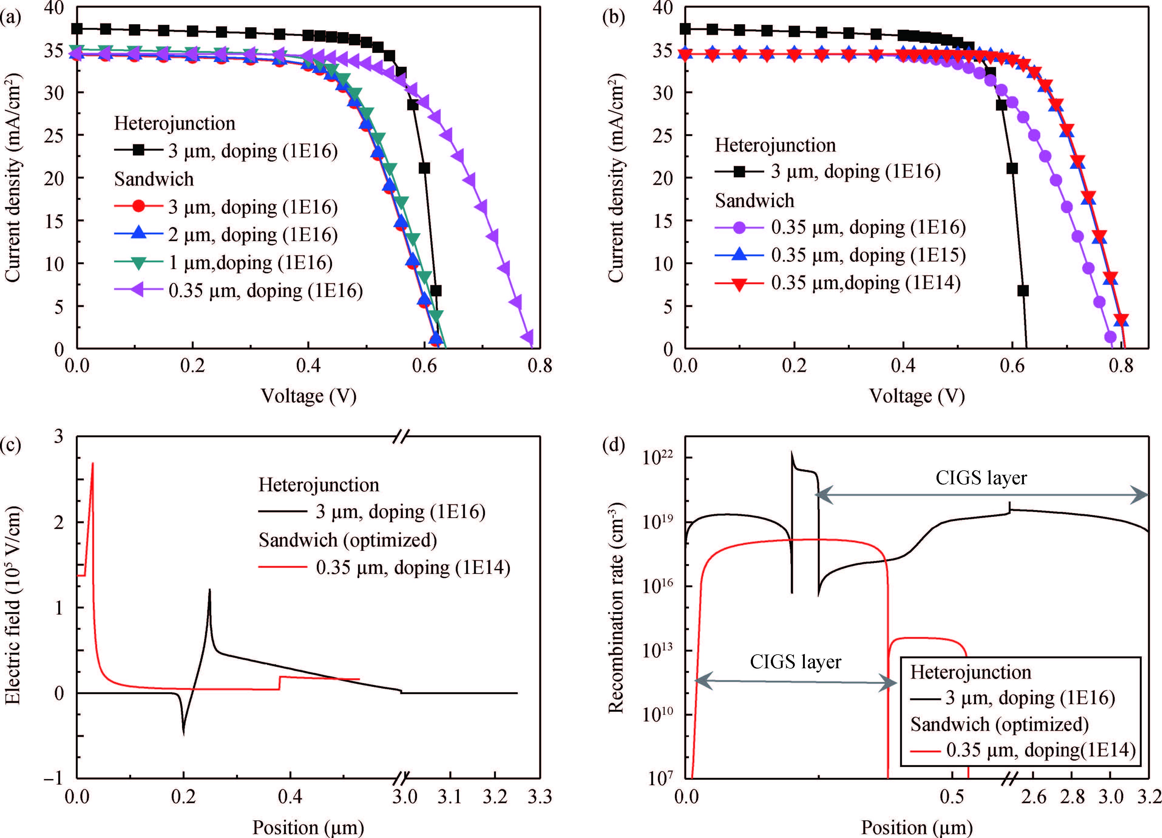
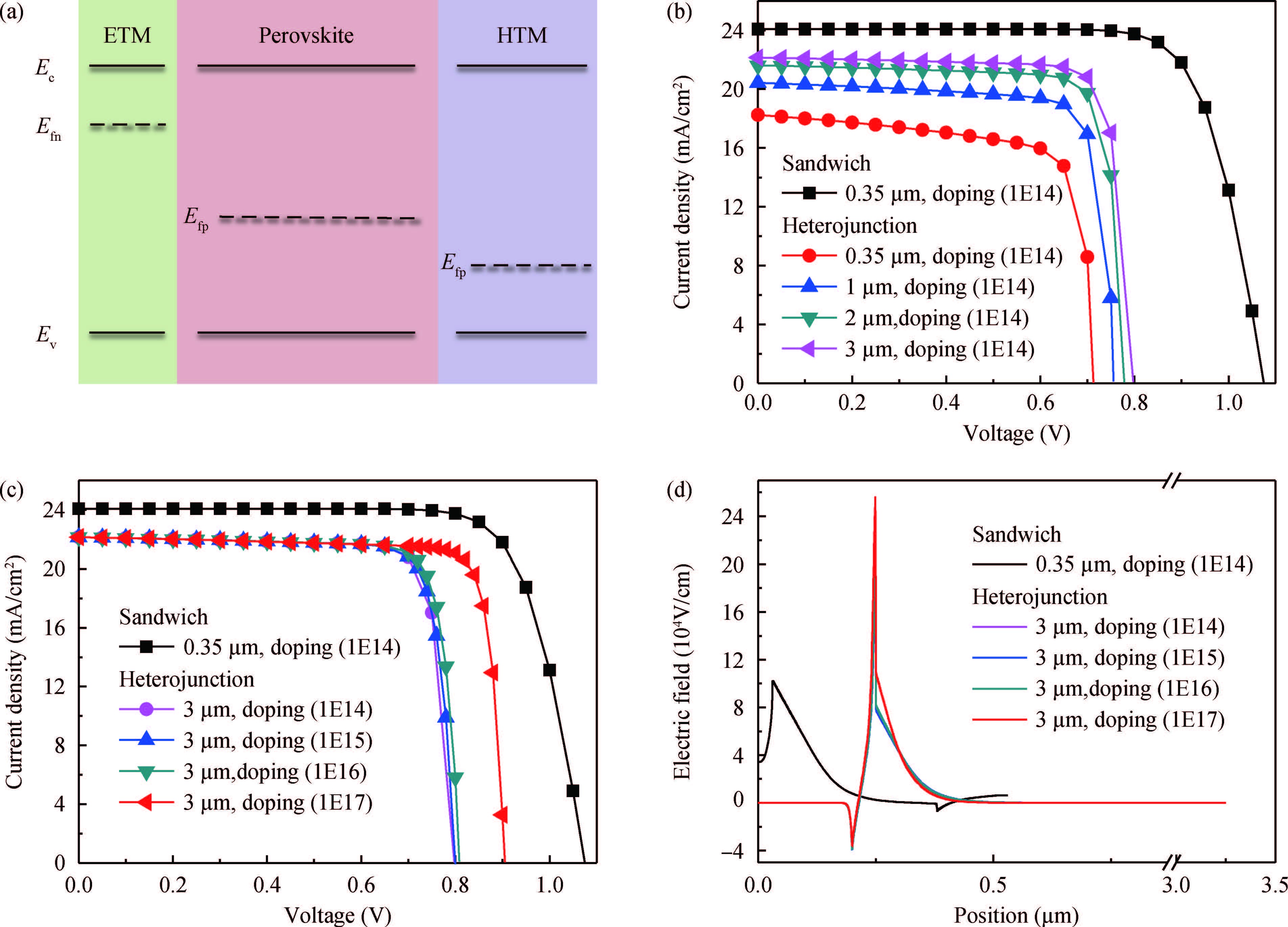
Table 1. wxAMPS parameters set for the standard perovskite solar cell.
| Parameter and unit | Compact TiO2 | CH3NH3PbI3 | Spiro-OMeTAD hline |
| ${{\varepsilon }_{r}}$ | 100 [18] | 30 [19] | 3 [20] |
| Eg (eV) | 3.2 | 1.55 [21] | 3.17 [20] |
| $\chi $ (eV) | 4 | 3.9 [22] | 2.05 [20] |
| Thickness (μm) | 0.03 | 0.35 | 0.15 |
| Na (cm-3) | 0 | 0 | 3 × 10¹⁸ |
| Nd (cm-3) | 5 × 10¹⁹ [18] | 0 | 0 |
| Nc (cm-3) | 1 × 10²¹ | 2.5 × 10²⁰ [23] | 2.8 × 10¹⁹ [24] |
| Nv (cm-3) | 1 × 10²¹ | 2.5 × 10²⁰ [22] | 1 × 10¹⁹ [24] |
 DownLoad: CSV
Table 2. wxAMPS parameters set for the standard CIGS solar cell [25].
| Parameter and unit | ZnO | CdS | CIGS |
| $\varepsilon_{\rm r}$ | 9 | 10 | 13.6 |
| Eg (eV) | 3.3 | 2.4 | 1.15 |
| $\chi $ (eV) | 4.4 | 4.2 | 4.5 |
| Thickness (μm) | 0.2 | 0.05 | 3 |
| Na (cm-3) | 0 | 0 | 2 × 10¹⁶ |
| Nd (cm-3) | 1 × 10¹⁸ | 1.1 × 10¹⁸ | 0 |
| Nc (cm-3) | 2.2 × 10¹⁸ | 2.2 × 10¹⁸ | 2.2 × 10¹⁸ |
| Nv (cm-3) | 1.8 × 10¹⁹ | 1.8 × 10¹⁹ | 1 × 10¹⁹ |
DownLoad: CSV
Table 3. Device performances of standard/ preliminary modulated CIGS and perovskite solar cells.
| Solar cells | Active layer property | JSC (mA cm-2) | VOC(V) | FF(%) | PCE (%) | |
| CIGS | Heterojunction | 3 μm, doping (1 × 10¹⁶) | 37.42 | 0.63 | 79.02 | 18.48 |
| Sandwich | 3 μm, doping (1 × 10¹⁶) | 34.34 | 0.62 | 65.74 | 14.09 | |
| Perovskite | Sandwich | 0.35 μm, doping (1 × 10¹⁴) | 24.08 | 1.08 | 76.13 | 19.71 |
| Heterojunction | 0.35 μm, doping (1 × 10¹⁴) | 18.24 | 0.71 | 73.79 | 9.6 |
DownLoad: CSV
| [1] |
Sandberg O J, Sundqvist A, Nyman M, et al. Relating charge transport, contact properties, and recombination to open-circuit voltage in sandwich-type thin-film solar cells. Phys Rev Appl, 2016, 5(4): 044005 doi: 10.1103/PhysRevApplied.5.044005
|
| [2] |
Yang Y, Chen W, Dou L T, et al. High-performance multiple-donor bulk heterojunction solar cells. Nat Photonics, 2015, 9(3): 190 doi: 10.1038/nphoton.2015.9
|
| [3] |
Wu Y M, Yang R X, Tian H M, et al. Photoelectric characteristics of CH3NH3PbI3/p-Si heterojunction. J Semicond, 2016, 37(5): 053002 doi: 10.1088/1674-4926/37/5/053002
|
| [4] |
Jin H H, Han H J, Lee M H, et al. Stable semi-transparent CH3NH3PbI3 planar sandwich solar cells. Energy Environ Sci, 2015, 8(10): 2922 doi: 10.1039/C5EE01050K
|
| [5] |
Wu W Q, Lei BX, Rao H S, et al. Hydrothermal fabrication of hierarchically anatase TiO2 nanowire arrays on FTO glass for dye-sensitized solar cells. Sci Rep, 2013, 3(2): 1352 https://www.researchgate.net/publication/235740345_Hydrothermal_Fabrication_of_Hierarchically_Anatase_TiO2_Nanowire_arrays_on_FTO_Glass_for_Dye-sensitized_Solar_Cells
|
| [6] |
Sim H, Lee J, Cho S, et al. A study on the band structure of ZnO/CdS heterojunction for CIGS solar-cell application. J Semicond Technol Sci, 2015, 15(2): 267 doi: 10.5573/JSTS.2015.15.2.267
|
| [7] |
Contreras M A, Nakada T, Hongo M, et al. ZnO/ZnS(O,OH)/Cu(In,Ga)Se2 Mo solar cell with 18.6% efficiency. Proceedings of World Conference on Photovoltaic Energy Conversion, 2003
|
| [8] |
Goetzberger A, Knobloch J, Voβ B, et al. The physics of solar cells. Imperial College Press, 2003: 384 http://cn.bing.com/academic/profile?id=eb0c728b296ec4a88349c72e297563fd&encoded=0&v=paper_preview&mkt=zh-cn
|
| [9] |
Minemoto T, Matsui T, Takakura H, et al. Theoretical analysis of the effect of conduction band offset of window/CIS layers on performance of CIS solar cells using device simulation. Sol Energy Materi Sol Cells, 2001, 67(1-4): 83 doi: 10.1016/S0927-0248(00)00266-X
|
| [10] | |
| [11] |
Nie W, Tsai H, Asadpour R, et al. High-efficiency solution-processed perovskite solar cells with millimeter-scale grains. Science, 2015, 347(6221): 522 doi: 10.1126/science.aaa0472
|
| [12] |
Wei D, Wang T Y, Ji J, et al. Photo-induced degradation of lead halide perovskite solar cells caused by the hole transport layer/metal electrode interface. J Mater Chem A, 2016, 4(5): 1991 doi: 10.1039/C5TA08622A
|
| [13] |
Chen W Z, Huang X, Cheng Q J, et al. Simulation analysis of heterojunction ZnO/CdS/Cu(In,Ga)Se2 thin-film solar cells using wxAMPS. Optik-Int J Light Electron Opt, 2015, 127: 182 https://www.researchgate.net/publication/284001321_Simulation_analysis_of_heterojunction_ZnOCdSCuInGaSe2_thin-film_solar_cells_using_wxAMPS
|
| [14] |
Liu Y M, Sun Y, Rockett A. A new simulation software of solar cells-wxAMPS. Sol Energy Mater Sol Cells, 2012, 98(1): 124 http://cn.bing.com/academic/profile?id=8c0d5d842344d77f2958ac4a37c24c82&encoded=0&v=paper_preview&mkt=zh-cn
|
| [15] |
Song D D, Wei D, Cui P, et al. Dual function interfacial layer for highly efficient and stable lead halide perovskite solar cells. J Mater Chem A, 2016, 4(16): 6091 doi: 10.1039/C6TA00577B
|
| [16] | |
| [17] |
De Wolf S, Holovsky J, Moon S J, et al. Organometallic halide perovskites: sharp optical absorption edge and its relation to photovoltaic performance. J Phys Chem Lett, 2014, 5(6): 1035 doi: 10.1021/jz500279b
|
| [18] |
Wojciechowski K, Saliba M, Leijtens T, et al. Sub-150℃ processed meso-superstructured perovskite solar cells with enhanced efficiency. Energy Environ Sci, 2014, 7(3): 1142 doi: 10.1039/C3EE43707H
|
| [19] |
Liu W Q, Zhang Y. Electrical characterization of TiO2/CH3 NH3PbI3 heterojunction solar cells. J Mater Chem A, 2014, 2(26): 10244 doi: 10.1039/c4ta01219d
|
| [20] |
Snaith H J, Gräzel M. Electron and hole transport through mesoporous TiO2 infiltrated with spiro-MeOTAD. Adv Mater, 2007, 19(21): 3643 doi: 10.1002/(ISSN)1521-4095
|
| [21] |
Noh J H, Sang H I, Jin H H, et al. Chemical management for colorful, efficient, and stable inorganic-organic hybrid nanostructured solar cells. Nano Lett, 2013, 13(4): 1764 doi: 10.1021/nl400349b
|
| [22] |
Laban W A, Etgar L. Depleted hole conductor-free lead halide iodide heterojunction solar cells. Energy Environ Sci, 2013, 6(11): 3249 doi: 10.1039/c3ee42282h
|
| [23] |
Stoumpos C C, Malliakas C D, Kanatzidis M G. Semiconducting tin and lead iodide perovskites with organic cations: phase transitions, high mobilities, and near-infrared photoluminescent properties. Inorg Chem, 2013, 52(15): 9019 doi: 10.1021/ic401215x
|
| [24] |
Fonash S J. Solar cell device physics. 2nd Ed. 2010
|
| [25] |
Liu Y M. Modeling of Cu(In,Ga)Se2 thin film solar cell device. Nankai University, 2012
|


Article views: 6151 Times PDF downloads: 57 Times Cited by: 0 Times
Received: 23 August 2016 Revised: 10 October 2016 Online: Published: 01 January 2017
| Citation: |
Tianyue Wang, Jiewei Chen, Gaoxiang Wu, Dandan Song, Meicheng Li. Designing novel thin film polycrystalline solar cells for high efficiency: sandwich CIGS and heterojunction perovskite[J]. Journal of Semiconductors, 2017, 38(1): 014005. doi: 10.1088/1674-4926/38/1/014005
****
T Y Wang, J W Chen, G X Wu, Dandan Song and A Song, M C Li. Designing novel thin film polycrystalline solar cells for high efficiency: sandwich CIGS and heterojunction perovskite[J]. J. Semicond., 2017, 38(1): 014005. doi: 10.1088/1674-4926/38/1/014005.

|
| [1] |
Sandberg O J, Sundqvist A, Nyman M, et al. Relating charge transport, contact properties, and recombination to open-circuit voltage in sandwich-type thin-film solar cells. Phys Rev Appl, 2016, 5(4): 044005 doi: 10.1103/PhysRevApplied.5.044005
|
| [2] |
Yang Y, Chen W, Dou L T, et al. High-performance multiple-donor bulk heterojunction solar cells. Nat Photonics, 2015, 9(3): 190 doi: 10.1038/nphoton.2015.9
|
| [3] |
Wu Y M, Yang R X, Tian H M, et al. Photoelectric characteristics of CH3NH3PbI3/p-Si heterojunction. J Semicond, 2016, 37(5): 053002 doi: 10.1088/1674-4926/37/5/053002
|
| [4] |
Jin H H, Han H J, Lee M H, et al. Stable semi-transparent CH3NH3PbI3 planar sandwich solar cells. Energy Environ Sci, 2015, 8(10): 2922 doi: 10.1039/C5EE01050K
|
| [5] |
Wu W Q, Lei BX, Rao H S, et al. Hydrothermal fabrication of hierarchically anatase TiO2 nanowire arrays on FTO glass for dye-sensitized solar cells. Sci Rep, 2013, 3(2): 1352 https://www.researchgate.net/publication/235740345_Hydrothermal_Fabrication_of_Hierarchically_Anatase_TiO2_Nanowire_arrays_on_FTO_Glass_for_Dye-sensitized_Solar_Cells
|
| [6] |
Sim H, Lee J, Cho S, et al. A study on the band structure of ZnO/CdS heterojunction for CIGS solar-cell application. J Semicond Technol Sci, 2015, 15(2): 267 doi: 10.5573/JSTS.2015.15.2.267
|
| [7] |
Contreras M A, Nakada T, Hongo M, et al. ZnO/ZnS(O,OH)/Cu(In,Ga)Se2 Mo solar cell with 18.6% efficiency. Proceedings of World Conference on Photovoltaic Energy Conversion, 2003
|
| [8] |
Goetzberger A, Knobloch J, Voβ B, et al. The physics of solar cells. Imperial College Press, 2003: 384 http://cn.bing.com/academic/profile?id=eb0c728b296ec4a88349c72e297563fd&encoded=0&v=paper_preview&mkt=zh-cn
|
| [9] |
Minemoto T, Matsui T, Takakura H, et al. Theoretical analysis of the effect of conduction band offset of window/CIS layers on performance of CIS solar cells using device simulation. Sol Energy Materi Sol Cells, 2001, 67(1-4): 83 doi: 10.1016/S0927-0248(00)00266-X
|
| [10] | |
| [11] |
Nie W, Tsai H, Asadpour R, et al. High-efficiency solution-processed perovskite solar cells with millimeter-scale grains. Science, 2015, 347(6221): 522 doi: 10.1126/science.aaa0472
|
| [12] |
Wei D, Wang T Y, Ji J, et al. Photo-induced degradation of lead halide perovskite solar cells caused by the hole transport layer/metal electrode interface. J Mater Chem A, 2016, 4(5): 1991 doi: 10.1039/C5TA08622A
|
| [13] |
Chen W Z, Huang X, Cheng Q J, et al. Simulation analysis of heterojunction ZnO/CdS/Cu(In,Ga)Se2 thin-film solar cells using wxAMPS. Optik-Int J Light Electron Opt, 2015, 127: 182 https://www.researchgate.net/publication/284001321_Simulation_analysis_of_heterojunction_ZnOCdSCuInGaSe2_thin-film_solar_cells_using_wxAMPS
|
| [14] |
Liu Y M, Sun Y, Rockett A. A new simulation software of solar cells-wxAMPS. Sol Energy Mater Sol Cells, 2012, 98(1): 124 http://cn.bing.com/academic/profile?id=8c0d5d842344d77f2958ac4a37c24c82&encoded=0&v=paper_preview&mkt=zh-cn
|
| [15] |
Song D D, Wei D, Cui P, et al. Dual function interfacial layer for highly efficient and stable lead halide perovskite solar cells. J Mater Chem A, 2016, 4(16): 6091 doi: 10.1039/C6TA00577B
|
| [16] | |
| [17] |
De Wolf S, Holovsky J, Moon S J, et al. Organometallic halide perovskites: sharp optical absorption edge and its relation to photovoltaic performance. J Phys Chem Lett, 2014, 5(6): 1035 doi: 10.1021/jz500279b
|
| [18] |
Wojciechowski K, Saliba M, Leijtens T, et al. Sub-150℃ processed meso-superstructured perovskite solar cells with enhanced efficiency. Energy Environ Sci, 2014, 7(3): 1142 doi: 10.1039/C3EE43707H
|
| [19] |
Liu W Q, Zhang Y. Electrical characterization of TiO2/CH3 NH3PbI3 heterojunction solar cells. J Mater Chem A, 2014, 2(26): 10244 doi: 10.1039/c4ta01219d
|
| [20] |
Snaith H J, Gräzel M. Electron and hole transport through mesoporous TiO2 infiltrated with spiro-MeOTAD. Adv Mater, 2007, 19(21): 3643 doi: 10.1002/(ISSN)1521-4095
|
| [21] |
Noh J H, Sang H I, Jin H H, et al. Chemical management for colorful, efficient, and stable inorganic-organic hybrid nanostructured solar cells. Nano Lett, 2013, 13(4): 1764 doi: 10.1021/nl400349b
|
| [22] |
Laban W A, Etgar L. Depleted hole conductor-free lead halide iodide heterojunction solar cells. Energy Environ Sci, 2013, 6(11): 3249 doi: 10.1039/c3ee42282h
|
| [23] |
Stoumpos C C, Malliakas C D, Kanatzidis M G. Semiconducting tin and lead iodide perovskites with organic cations: phase transitions, high mobilities, and near-infrared photoluminescent properties. Inorg Chem, 2013, 52(15): 9019 doi: 10.1021/ic401215x
|
| [24] |
Fonash S J. Solar cell device physics. 2nd Ed. 2010
|
| [25] |
Liu Y M. Modeling of Cu(In,Ga)Se2 thin film solar cell device. Nankai University, 2012
|

 WeChat ID
Journal of Semiconductors © 2017 All Rights Reserved 京ICP备05085259号-2


