


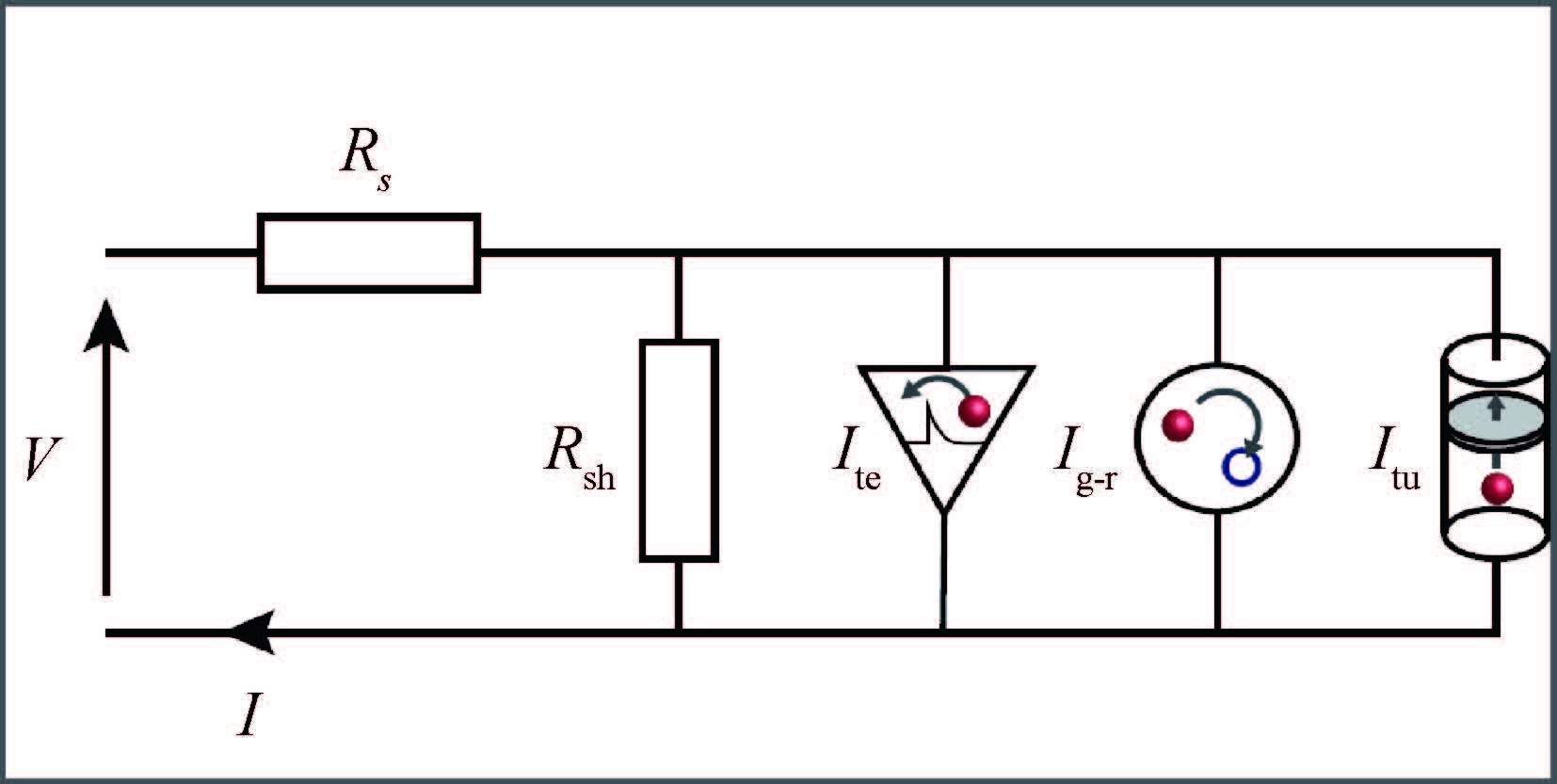
Fig. 1.
Electrical equivalent model with all the defined conduction phenomena.
SEMICONDUCTOR DEVICES
O. Latry, A. Divay, D. Fadil and P. Dherbécourt
Corresponding author: O. Latry,Email:olivier.latry@univ-rouen.fr
Abstract: Electrical characterization analyses are proposed in this work using the Lambert function on Schottky junctions in GaN wide band gap semiconductor devices for extraction of physical parameters. The Lambert function is used to give an explicit expression of the current in the Schottky junction. This function is applied with defined conduction phenomena, whereas other work presented arbitrary (or undefined) conduction mechanisms in such parameters' extractions. Based upon AlGaN/GaN HEMT structures, extractions of parameters are undergone in order to provide physical characteristics. This work highlights a new expression of current with defined conduction phenomena in order to quantify the physical properties of Schottky contacts in AlGaN/GaN HEMT transistors.
Keywords: GaN, Schottky junction, conduction mechanisms, Lambert function, parameters extraction
| [1] |
Norde H. A modified forward I-V plot for Schottky diodes with high series resistance. J Appl Phys, 1979, 50(7): 5052 doi: 10.1063/1.325607
|
| [2] |
Cheung S K, Cheung N W. Extraction of Schottky diode parameters from forward current voltage characteristics. Appl Phys Lett, 1986, 49(2): 85 doi: 10.1063/1.97359
|
| [3] |
Werner J H, Guttler H H. Barrier inhomogeneities at Schottky contacts. J Appl Phys, 1991, 69(3): 1522 doi: 10.1063/1.347243
|
| [4] |
Lee T C, Fung S, Beling C D, et al. A systematic approach to the measurement of ideality factor, series resistance, and barrier height for Schottky diodes. J Appl Phys, 1992, 72(10): 4739 doi: 10.1063/1.352082
|
| [5] |
Ayyildiz E, Turut A, Efeoglu H, et al. Effect of series resistance on the forward current-voltage characteristics of Schottky diodes in the presence of interfacial layer. Solid-State Electron, 1996, 39(1): 83 doi: 10.1016/0038-1101(95)00093-9
|
| [6] |
Osvald J, Dobrocka E. Generalized approach to the parameter extraction from IV characteristics of Schottky diodes. Semicond Sci Technol, 1996, 11(8): 1198 doi: 10.1088/0268-1242/11/8/014
|
| [7] |
Ortiz-Conde A, Ma Y, Thomson J, et al. Parameter extraction using lateral and vertical optimization. 22nd International Conference on Microelectronics, 2000, 1: 165 http://cn.bing.com/academic/profile?id=b21722efbd52a2e4223638990b98e71d&encoded=0&v=paper_preview&mkt=zh-cn
|
| [8] |
Tung R T. Electron transport at metal-semiconductor interfaces: general theory. Phys Rev B, 1992, 45(23): 13509 doi: 10.1103/PhysRevB.45.13509
|
| [9] |
Tung R T. Recent advances in Schottky barrier concepts. Mater Sci Eng R, 2001, 35(1-3): 1 doi: 10.1016/S0927-796X(01)00037-7
|
| [10] |
Ortiz-Conde A, Ma Y S, Thomson J, et al. Direct extraction of semiconductor device parameters using lateral optimization method. Solid-State Electron, 1999, 43: 845 doi: 10.1016/S0038-1101(99)00044-1
|
| [11] |
Ortiz-Conde A, Garcia-Sanchez F J, Muci J. New method to extract the model parameters of solar cells from the explicit analytic solutions of their illuminated I-V characteristics. Sol Energy Mater Sol Cells, 2006, 90(3): 352 doi: 10.1016/j.solmat.2005.04.023
|
| [12] |
Corless R M. On the Lambert W function. Research report. University of Waterloo, Computer Science Department, 1993
|
| [13] |
Munoz D L, Muci J, Ortiz-Conde A, et al. An explicit multi exponential model for semiconductor junctions with series and shunt resistances. Microelectron Reliab, 2011, 51(12): 2044 doi: 10.1016/j.microrel.2011.06.030
|
| [14] |
Arslan E, Altndal E, Özçelik S, et al. Tunneling current via dislocations in Schottky diodes on AlInN/AlN/GaN heterostructures. Semicond Sci Technol, 2009, 24(7): 075003 doi: 10.1088/0268-1242/24/7/075003
|
| [15] |
Qiao D, Yu L S, Lau S S, et al. Dependence of Ni/AlGaN Schottky barrier height on Al mole fraction. J Appl Phys, 2000, 87(2): 801 doi: 10.1063/1.371944
|
| [16] |
Fonder J B, Chevalier L, Genevois C, et al. Physical analysis of Schottky contact on power AlGaN/GaN HEMT after pulsed-RF life test. Microelectron Reliab, 2012, 52(9/10): 2205 http://cn.bing.com/academic/profile?id=172fe52a4b90d080d0c2e31ed0619660&encoded=0&v=paper_preview&mkt=zh-cn
|
| [17] |
Denis P, Dherbécourt P, Latry O, et al. Robustness of 4H-SiC 1200 V Schottky diodes under high electrostatic discharge like human body model stresses: an in-depth failure analysis. Diamond Relat Mater, 2014, 44: 62 doi: 10.1016/j.diamond.2014.02.002
|
| [18] |
Arslan E, Alt E, Özçelik S, et al. Dislocation-governed current-transport mechanism in (Ni/Au)-AlGaN/AlN/GaN heterostructures. J Appl Phys, 2009, 105(2): 023705 doi: 10.1063/1.3068202
|
| [19] |
Saadaoui S, Ben Salem M M, Gassoumi M, et al. Electrical characterization of (Ni/Au)/Al0.25Ga0.75N/GaN/SiC Schottky barrier diode. J Appl Phys, 2011, 110(1): 013701 doi: 10.1063/1.3600229
|
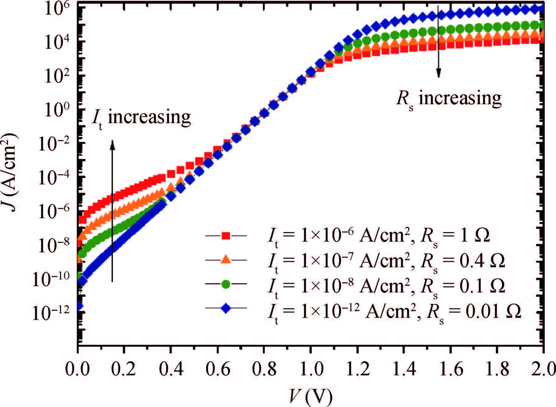
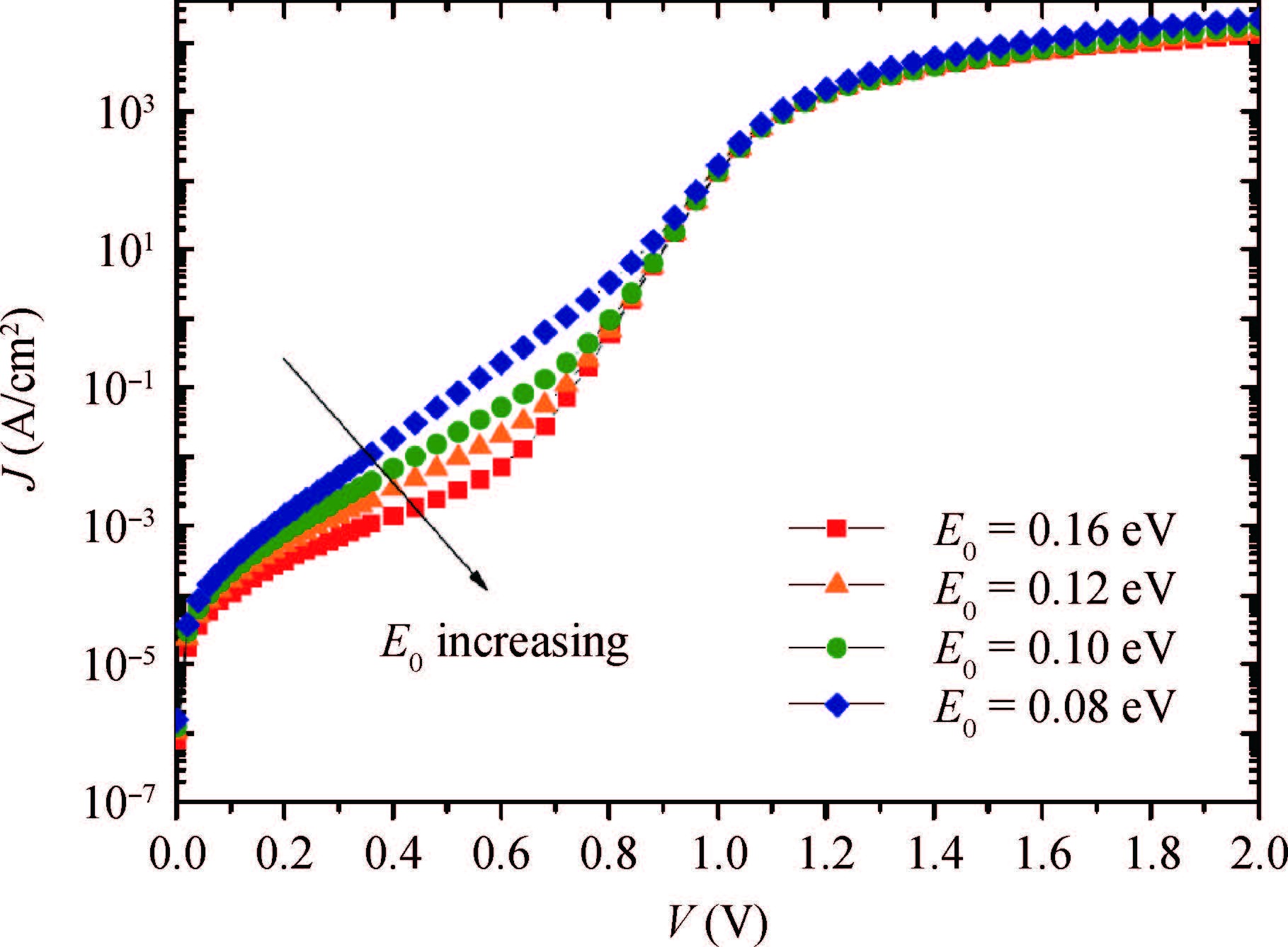

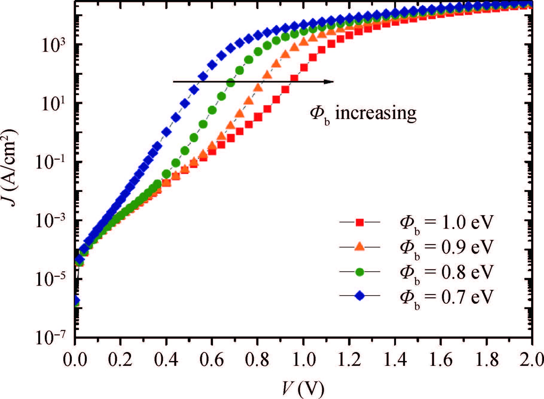
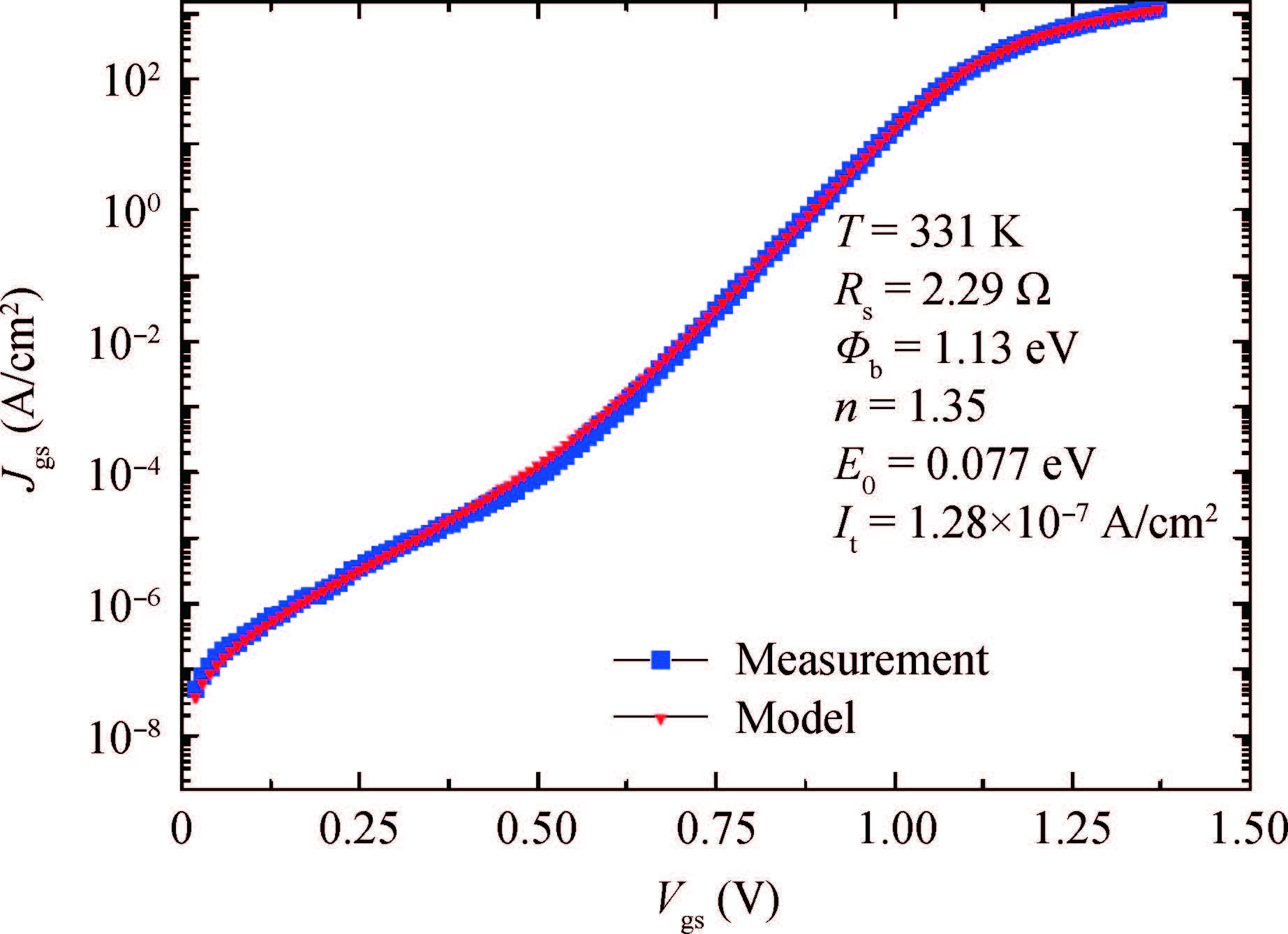
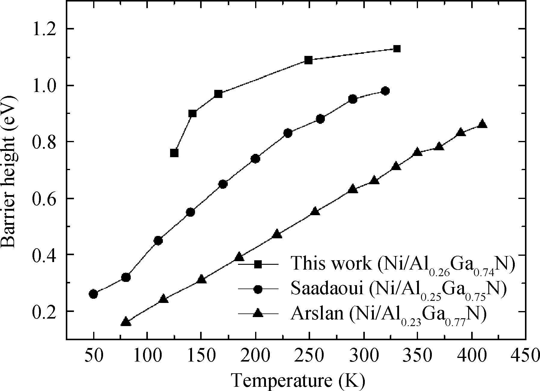
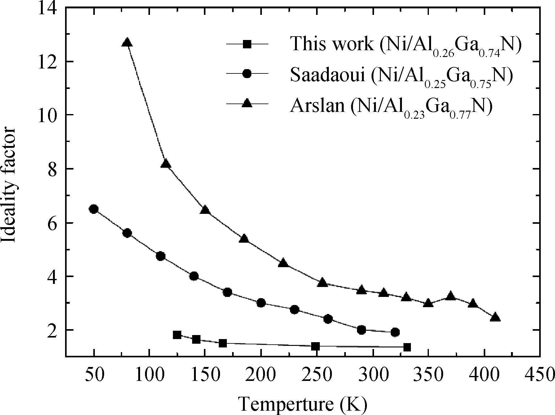
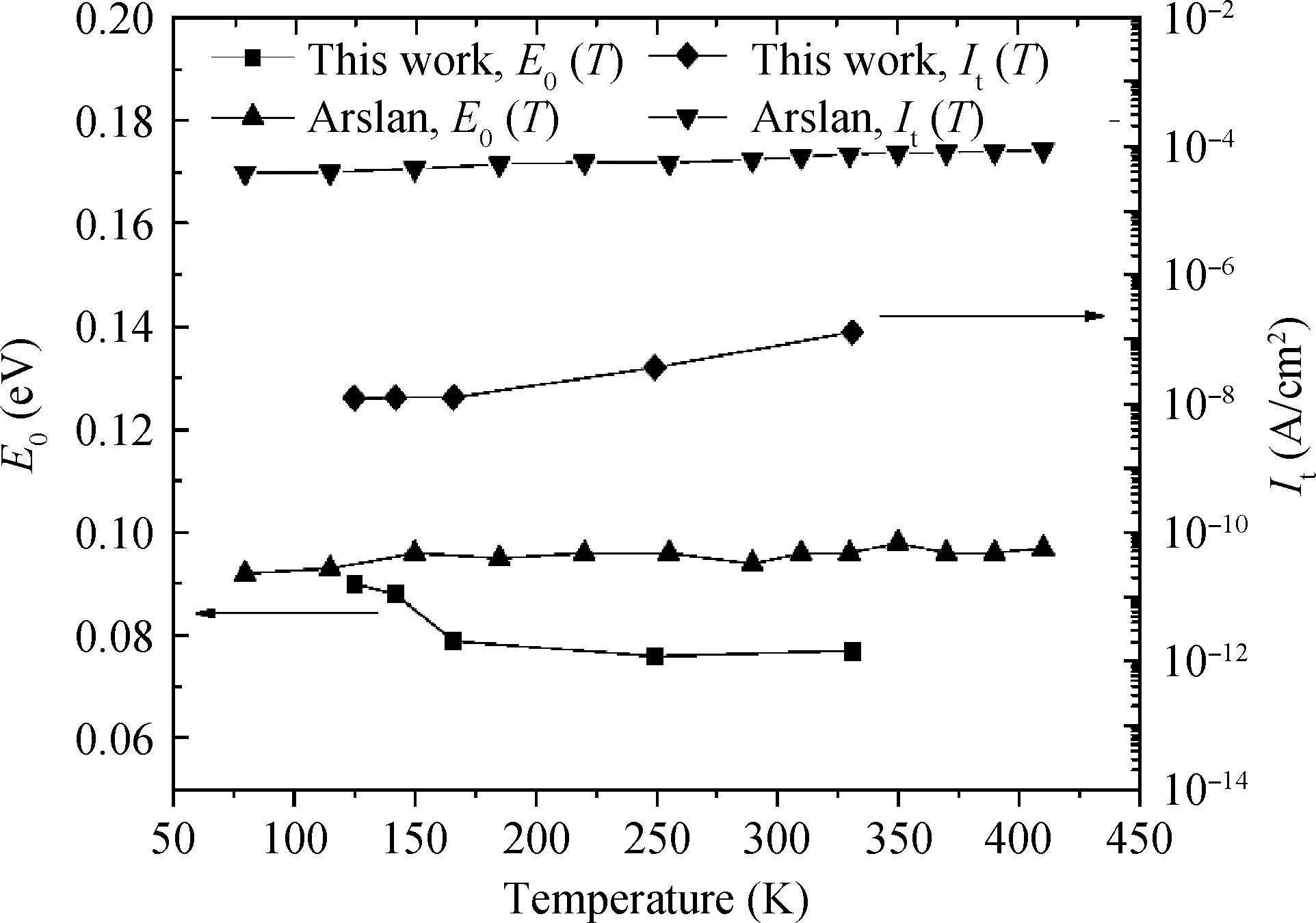
Table 1. Summary of Ni/AlGaN Schottky parameters extraction using the Lambert function in AlGaN/GaN HEMT devices with defined conduction phenomena.
| T (K) | $\Phi_{\mathrm{b}}$ (eV) | n | Rs(Ω) | It (A/cm2) | $E_{0} $ (eV) |
| 125 | 0.76 | 1.81 | 3.71 | 1.23 × 10⁻⁸ | 0.09 |
| 142 | 0.9 | 1.63 | 3.23 | 1.24 × 10⁻⁸ | 0.088 |
| 166 | 0.97 | 1.5 | 1.52 | 1.24 × 10⁻⁸ | 0.079 |
| 249 | 1.09 | 1.38 | 3 | 3.62 × 10⁻⁸ | 0.076 |
| 331 | 1.13 | 1.35 | 2.28 | 1.29 × 10⁻⁷ | 0.077 |
 DownLoad: CSV
| [1] |
Norde H. A modified forward I-V plot for Schottky diodes with high series resistance. J Appl Phys, 1979, 50(7): 5052 doi: 10.1063/1.325607
|
| [2] |
Cheung S K, Cheung N W. Extraction of Schottky diode parameters from forward current voltage characteristics. Appl Phys Lett, 1986, 49(2): 85 doi: 10.1063/1.97359
|
| [3] |
Werner J H, Guttler H H. Barrier inhomogeneities at Schottky contacts. J Appl Phys, 1991, 69(3): 1522 doi: 10.1063/1.347243
|
| [4] |
Lee T C, Fung S, Beling C D, et al. A systematic approach to the measurement of ideality factor, series resistance, and barrier height for Schottky diodes. J Appl Phys, 1992, 72(10): 4739 doi: 10.1063/1.352082
|
| [5] |
Ayyildiz E, Turut A, Efeoglu H, et al. Effect of series resistance on the forward current-voltage characteristics of Schottky diodes in the presence of interfacial layer. Solid-State Electron, 1996, 39(1): 83 doi: 10.1016/0038-1101(95)00093-9
|
| [6] |
Osvald J, Dobrocka E. Generalized approach to the parameter extraction from IV characteristics of Schottky diodes. Semicond Sci Technol, 1996, 11(8): 1198 doi: 10.1088/0268-1242/11/8/014
|
| [7] |
Ortiz-Conde A, Ma Y, Thomson J, et al. Parameter extraction using lateral and vertical optimization. 22nd International Conference on Microelectronics, 2000, 1: 165 http://cn.bing.com/academic/profile?id=b21722efbd52a2e4223638990b98e71d&encoded=0&v=paper_preview&mkt=zh-cn
|
| [8] |
Tung R T. Electron transport at metal-semiconductor interfaces: general theory. Phys Rev B, 1992, 45(23): 13509 doi: 10.1103/PhysRevB.45.13509
|
| [9] |
Tung R T. Recent advances in Schottky barrier concepts. Mater Sci Eng R, 2001, 35(1-3): 1 doi: 10.1016/S0927-796X(01)00037-7
|
| [10] |
Ortiz-Conde A, Ma Y S, Thomson J, et al. Direct extraction of semiconductor device parameters using lateral optimization method. Solid-State Electron, 1999, 43: 845 doi: 10.1016/S0038-1101(99)00044-1
|
| [11] |
Ortiz-Conde A, Garcia-Sanchez F J, Muci J. New method to extract the model parameters of solar cells from the explicit analytic solutions of their illuminated I-V characteristics. Sol Energy Mater Sol Cells, 2006, 90(3): 352 doi: 10.1016/j.solmat.2005.04.023
|
| [12] |
Corless R M. On the Lambert W function. Research report. University of Waterloo, Computer Science Department, 1993
|
| [13] |
Munoz D L, Muci J, Ortiz-Conde A, et al. An explicit multi exponential model for semiconductor junctions with series and shunt resistances. Microelectron Reliab, 2011, 51(12): 2044 doi: 10.1016/j.microrel.2011.06.030
|
| [14] |
Arslan E, Altndal E, Özçelik S, et al. Tunneling current via dislocations in Schottky diodes on AlInN/AlN/GaN heterostructures. Semicond Sci Technol, 2009, 24(7): 075003 doi: 10.1088/0268-1242/24/7/075003
|
| [15] |
Qiao D, Yu L S, Lau S S, et al. Dependence of Ni/AlGaN Schottky barrier height on Al mole fraction. J Appl Phys, 2000, 87(2): 801 doi: 10.1063/1.371944
|
| [16] |
Fonder J B, Chevalier L, Genevois C, et al. Physical analysis of Schottky contact on power AlGaN/GaN HEMT after pulsed-RF life test. Microelectron Reliab, 2012, 52(9/10): 2205 http://cn.bing.com/academic/profile?id=172fe52a4b90d080d0c2e31ed0619660&encoded=0&v=paper_preview&mkt=zh-cn
|
| [17] |
Denis P, Dherbécourt P, Latry O, et al. Robustness of 4H-SiC 1200 V Schottky diodes under high electrostatic discharge like human body model stresses: an in-depth failure analysis. Diamond Relat Mater, 2014, 44: 62 doi: 10.1016/j.diamond.2014.02.002
|
| [18] |
Arslan E, Alt E, Özçelik S, et al. Dislocation-governed current-transport mechanism in (Ni/Au)-AlGaN/AlN/GaN heterostructures. J Appl Phys, 2009, 105(2): 023705 doi: 10.1063/1.3068202
|
| [19] |
Saadaoui S, Ben Salem M M, Gassoumi M, et al. Electrical characterization of (Ni/Au)/Al0.25Ga0.75N/GaN/SiC Schottky barrier diode. J Appl Phys, 2011, 110(1): 013701 doi: 10.1063/1.3600229
|


Article views: 4342 Times PDF downloads: 57 Times Cited by: 0 Times
Received: 30 August 2016 Revised: 31 October 2016 Online: Published: 01 January 2017
| Citation: |
O. Latry, A. Divay, D. Fadil, P. Dherbécourt. Extraction of physical Schottky parameters using the Lambert function in Ni/AlGaN/GaN HEMT devices with defined conduction phenomena[J]. Journal of Semiconductors, 2017, 38(1): 014007. doi: 10.1088/1674-4926/38/1/014007
****
O. Latry, A. Divay, D. Fadil, P. Dherbécourt. Extraction of physical Schottky parameters using the Lambert function in Ni/AlGaN/GaN HEMT devices with defined conduction phenomena[J]. J. Semicond., 2017, 38(1): 014007. doi: 10.1088/1674-4926/38/1/014007.

|
| [1] |
Norde H. A modified forward I-V plot for Schottky diodes with high series resistance. J Appl Phys, 1979, 50(7): 5052 doi: 10.1063/1.325607
|
| [2] |
Cheung S K, Cheung N W. Extraction of Schottky diode parameters from forward current voltage characteristics. Appl Phys Lett, 1986, 49(2): 85 doi: 10.1063/1.97359
|
| [3] |
Werner J H, Guttler H H. Barrier inhomogeneities at Schottky contacts. J Appl Phys, 1991, 69(3): 1522 doi: 10.1063/1.347243
|
| [4] |
Lee T C, Fung S, Beling C D, et al. A systematic approach to the measurement of ideality factor, series resistance, and barrier height for Schottky diodes. J Appl Phys, 1992, 72(10): 4739 doi: 10.1063/1.352082
|
| [5] |
Ayyildiz E, Turut A, Efeoglu H, et al. Effect of series resistance on the forward current-voltage characteristics of Schottky diodes in the presence of interfacial layer. Solid-State Electron, 1996, 39(1): 83 doi: 10.1016/0038-1101(95)00093-9
|
| [6] |
Osvald J, Dobrocka E. Generalized approach to the parameter extraction from IV characteristics of Schottky diodes. Semicond Sci Technol, 1996, 11(8): 1198 doi: 10.1088/0268-1242/11/8/014
|
| [7] |
Ortiz-Conde A, Ma Y, Thomson J, et al. Parameter extraction using lateral and vertical optimization. 22nd International Conference on Microelectronics, 2000, 1: 165 http://cn.bing.com/academic/profile?id=b21722efbd52a2e4223638990b98e71d&encoded=0&v=paper_preview&mkt=zh-cn
|
| [8] |
Tung R T. Electron transport at metal-semiconductor interfaces: general theory. Phys Rev B, 1992, 45(23): 13509 doi: 10.1103/PhysRevB.45.13509
|
| [9] |
Tung R T. Recent advances in Schottky barrier concepts. Mater Sci Eng R, 2001, 35(1-3): 1 doi: 10.1016/S0927-796X(01)00037-7
|
| [10] |
Ortiz-Conde A, Ma Y S, Thomson J, et al. Direct extraction of semiconductor device parameters using lateral optimization method. Solid-State Electron, 1999, 43: 845 doi: 10.1016/S0038-1101(99)00044-1
|
| [11] |
Ortiz-Conde A, Garcia-Sanchez F J, Muci J. New method to extract the model parameters of solar cells from the explicit analytic solutions of their illuminated I-V characteristics. Sol Energy Mater Sol Cells, 2006, 90(3): 352 doi: 10.1016/j.solmat.2005.04.023
|
| [12] |
Corless R M. On the Lambert W function. Research report. University of Waterloo, Computer Science Department, 1993
|
| [13] |
Munoz D L, Muci J, Ortiz-Conde A, et al. An explicit multi exponential model for semiconductor junctions with series and shunt resistances. Microelectron Reliab, 2011, 51(12): 2044 doi: 10.1016/j.microrel.2011.06.030
|
| [14] |
Arslan E, Altndal E, Özçelik S, et al. Tunneling current via dislocations in Schottky diodes on AlInN/AlN/GaN heterostructures. Semicond Sci Technol, 2009, 24(7): 075003 doi: 10.1088/0268-1242/24/7/075003
|
| [15] |
Qiao D, Yu L S, Lau S S, et al. Dependence of Ni/AlGaN Schottky barrier height on Al mole fraction. J Appl Phys, 2000, 87(2): 801 doi: 10.1063/1.371944
|
| [16] |
Fonder J B, Chevalier L, Genevois C, et al. Physical analysis of Schottky contact on power AlGaN/GaN HEMT after pulsed-RF life test. Microelectron Reliab, 2012, 52(9/10): 2205 http://cn.bing.com/academic/profile?id=172fe52a4b90d080d0c2e31ed0619660&encoded=0&v=paper_preview&mkt=zh-cn
|
| [17] |
Denis P, Dherbécourt P, Latry O, et al. Robustness of 4H-SiC 1200 V Schottky diodes under high electrostatic discharge like human body model stresses: an in-depth failure analysis. Diamond Relat Mater, 2014, 44: 62 doi: 10.1016/j.diamond.2014.02.002
|
| [18] |
Arslan E, Alt E, Özçelik S, et al. Dislocation-governed current-transport mechanism in (Ni/Au)-AlGaN/AlN/GaN heterostructures. J Appl Phys, 2009, 105(2): 023705 doi: 10.1063/1.3068202
|
| [19] |
Saadaoui S, Ben Salem M M, Gassoumi M, et al. Electrical characterization of (Ni/Au)/Al0.25Ga0.75N/GaN/SiC Schottky barrier diode. J Appl Phys, 2011, 110(1): 013701 doi: 10.1063/1.3600229
|

 WeChat ID
Journal of Semiconductors © 2017 All Rights Reserved 京ICP备05085259号-2


