


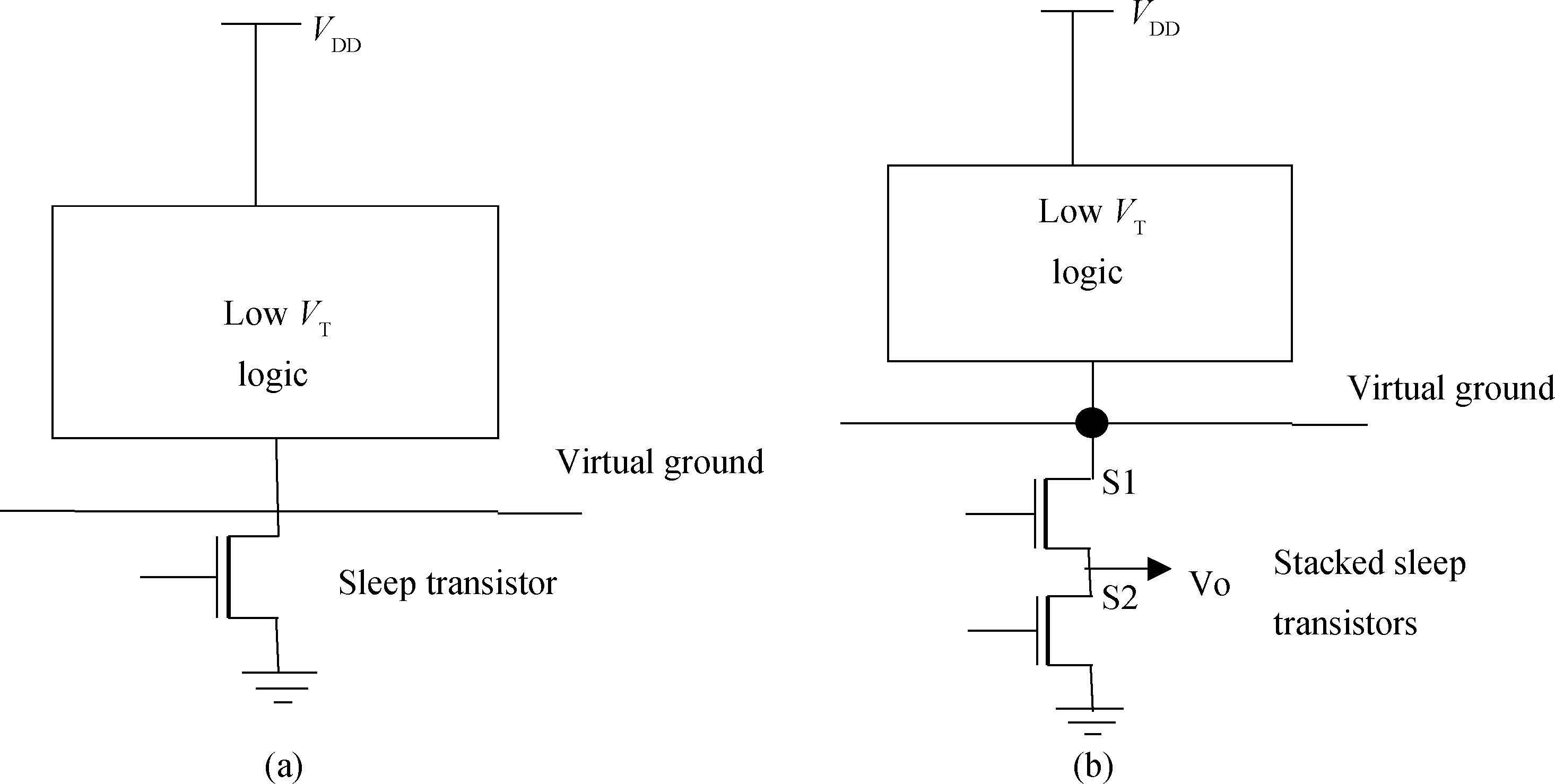
Fig. 1.
(a) Representation of conventional MTCMOS power-gating structure. (b) MTCMOS with stacked sleep transistor.
SEMICONDUCTOR INTEGRATED CIRCUITS
Rumi Rastogi and Sujata Pandey
Corresponding author: Sujata Pandey,Email:rumi.ravi@gmail.com,spandey@amity.edu
Abstract: In this paper we have investigated the single phase sleep signal modulation technique, step-wise Vgs technique and the three-phase reactivation technique to evaluate the noise characteristics of multi-threshold CMOS circuits used in communication systems. The stacking technique is also implemented in this paper for the sleep transistor. The stacking approach helps to minimize leakage power. The mode transition noise minimization techniques have been applied to 32-bit dynamic TSPC adder with stacked sleep transistors in a standard 45-nm CMOS process. The reactivation noise, delay and energy consumption of all the three techniques have been evaluated. It has been shown that the three phase modulation technique significantly minimizes the reactivation delay when the peak noise level is maintained the same for all three techniques. The three phase modulation technique shows 67.3% and 35% reduction in delay compared to the single phase and step-wise Vgs modulation techniques respectively. The reactivation energy is also suppressed by 49.3% and 39.14% with respect to the single-phase and stepwise Vgs techniques.
Keywords: MTCMOS, noise tolerant, low power
| [1] |
Chowdhury M A J, Rizwan M S, Islam M S. An efficient VLSI design approach to reduce static power using variable body biasing. Int J Electron Comput Energ Electron Commun Eng, 2012, 6(4): 2012 http://waset.org/publications/8289/an-efficient-vlsi-design-approach-to-reduce-static-power-using-variable-body-biasing
|
| [2] |
Jiao H, Kursun V. Reactivation noise suppression with sleep signal slew rate modulation in MTCMOS circuits. IEEE Trans VLSI Syst, 2013, 21(3): 533 doi: 10.1109/TVLSI.2012.2190116
|
| [3] |
Calhoun B H, Honoré F A, Chandrakasan A P. A leakage reduction methodology for distributed MTCMOS. IEEE J Solid-State Circuits, 2004, 39(5): 818 doi: 10.1109/JSSC.2004.826335
|
| [4] |
Jiao H, Kursun V. Ground-bouncing-noise-aware combinational MTCMOS circuits. IEEE Trans Circuits Syst I, 2011, 57(8): 2053 http://cn.bing.com/academic/profile?id=57f49ececdbe3958af46a6c3e5a3d99a&encoded=0&v=paper_preview&mkt=zh-cn
|
| [5] |
Jiao H, Kursun V. Threshold voltage tuning for faster activation with lower noise in tri-mode MTCMOS circuits. IEEE Trans VLSI Syst, 2012, 20(4): 741 doi: 10.1109/TVLSI.2011.2110663
|
| [6] |
Heydari P, Pedram M. Ground bounce in digital VLSI circuits. IEEE Trans VLSI Syst, 2003, 11(2): 180 doi: 10.1109/TVLSI.2003.810785
|
| [7] |
Kurd N, Bhamidipati S, Mozak C, et al. A family of 32 nm IA processors. IEEE J Solid-State Circuits, 2011, 46(1): 119 doi: 10.1109/JSSC.2010.2079430
|
| [8] |
Kim S, Kosonocky V, Knebel D R, et al. Minimizing inductive noise in system-on-a-chip with multiple power gating structures. IEEE Eur Solid-State Circuits Conf, 2003: 635 http://cn.bing.com/academic/profile?id=fb44445d9bedd4cbda6bf85e228b5e37&encoded=0&v=paper_preview&mkt=zh-cn
|
| [9] |
Rastogi R, Pandey S. Implementing low power dynamic adders in MTCMOS technology. IEEE International Conference on Electronics and Communication Systems, 2015: 782 http://cn.bing.com/academic/profile?id=a764f91386b17d54e0f0c214904b63ba&encoded=0&v=paper_preview&mkt=zh-cn
|
| [10] |
Rastogi R, Pandey S. Leakage power reduction in MTCMOS based high speed adders. IEEE International Conference on Computer, Communication and Control, 2015: 1 http://cn.bing.com/academic/profile?id=6ab53740be3e91a2a7e4048225295fd9&encoded=0&v=paper_preview&mkt=zh-cn
|
| [11] |
DeepakSubramanyan B S, Nuñez A. Analysis of subthreshold leakage reduction in CMOS digital circuits. Proceedings of the 13th NASA VLSI Symposium, 2007: 1400 https://www.researchgate.net/publication/224310148_Analysis_of_subthreshold_leakage_reduction_in_CMOS_digital_circuits
|
| [12] |
Mukhopadhyay S, Neau C, Cakici R T, et al. Gate leakage reduction for scaled devices using transistor stacking. IEEE Trans VLSI Syst, 2003, 11(4): 716 doi: 10.1109/TVLSI.2003.816145
|
| [13] |
Kim S, Kosonocky S V, Knebele D R, et al. A multi-mode power gating structure for low-voltage deep-submicron CMOS ICs. IEEE Trans Circuits Syst II, 2007, 54(7): 586 doi: 10.1109/TCSII.2007.894428
|


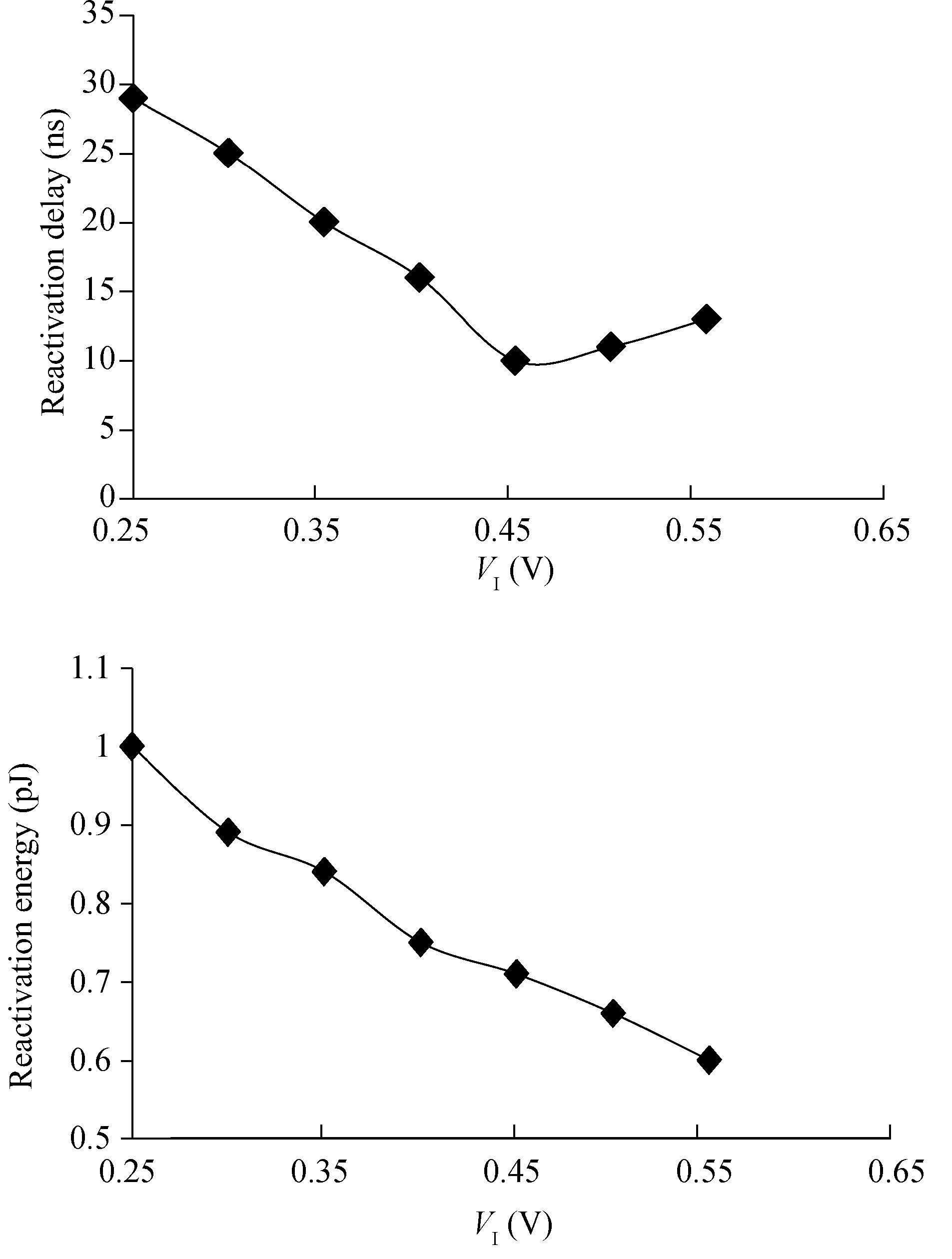

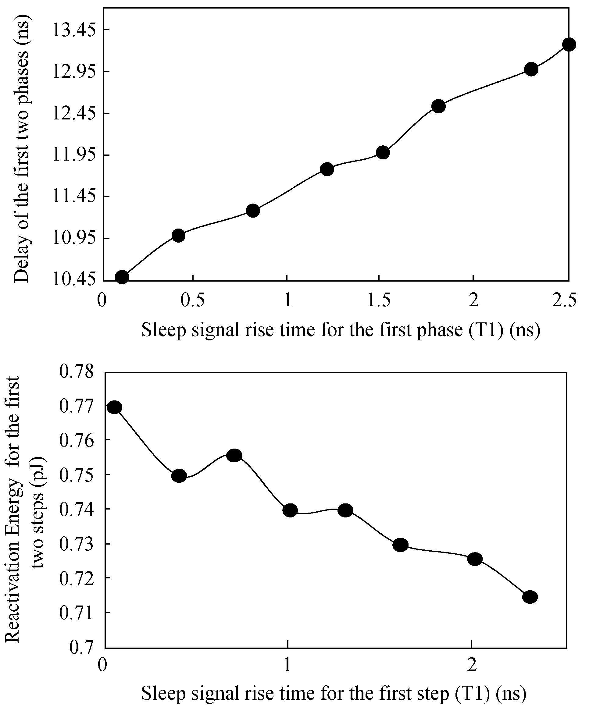
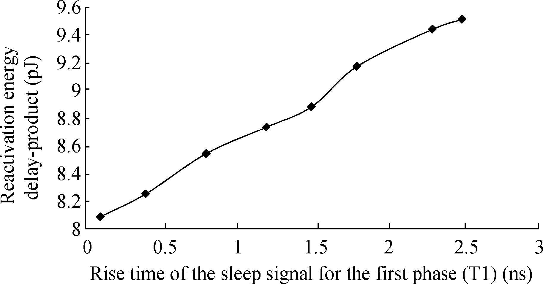
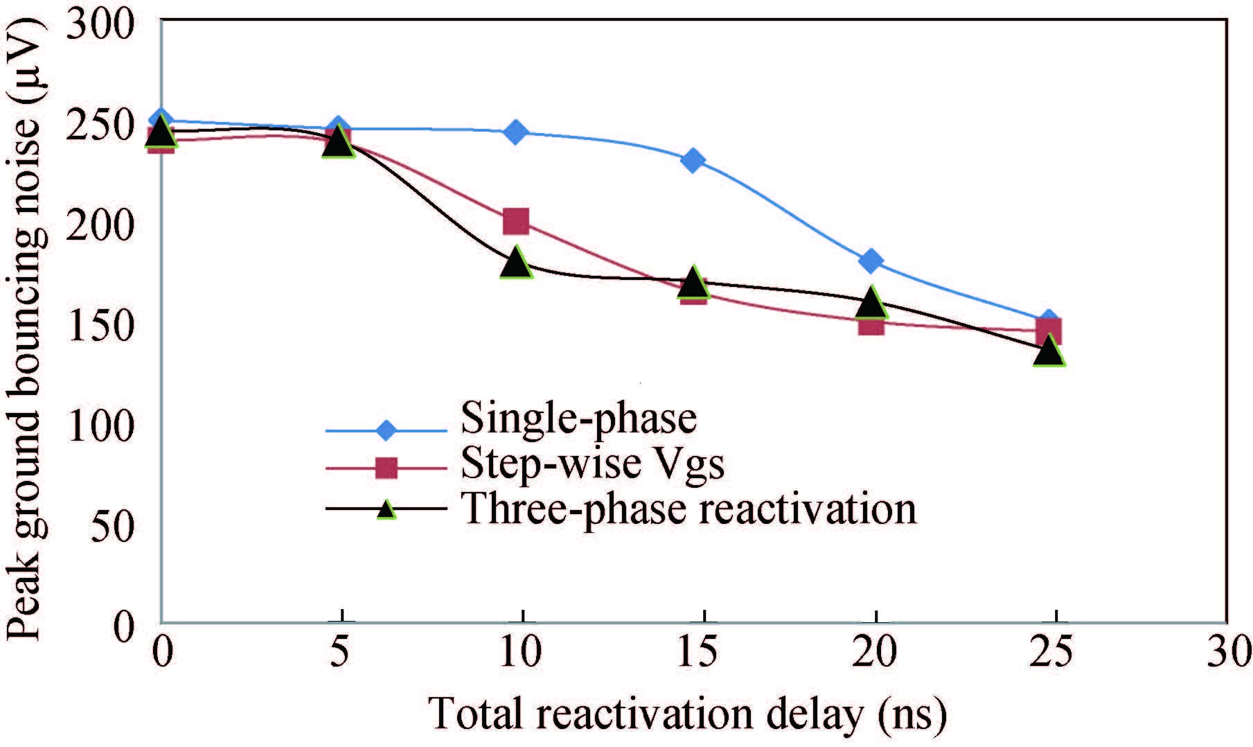
Table 1. Evaluation of different sleep signal modulation techniques.
| Reactivation technique | Single-phase | Step-wise Vgs | Three-phase |
| Peak reactivation noise (μV) | 200 | 228 | 197 |
| Reactivation delay (ns) | 35.38 | 17.63 | 11.56 |
| Reactivation energy (pJ) | 0.785 | 0.654 | 0.398 |
| Leakage power (nW) | 56.49 | 67.54 | 67.02 |
 DownLoad: CSV
Table 2. Comparison of the proposed techniques with other existing techniques for noise minimization.
| Circuit technique | Peak reactivationpar noise (μV) | Reactivation delaypar (ns) | Reactivationpar energy (pJ) | Leakage powerpar (nW) |
| Standard gated ground [4] | 326 | 8.5 | 2.11 | 60.1 |
| Standard tri-mode [13] | 220 | 21.24 | 0.854 | 67.3 |
| Tri-mode with low-Vth Parker (TML) [5] | 215 | 20.65 | 0.774 | 68 |
| Tri-mode with forward body-biased Parker [5] | 203 | 18.33 | 0.553 | 65.45 |
| Simple stacking without modulation [11] | 258 | 16 | 0.886 | 66.34 |
| Proposed (three phase clock with stack) | 197 | 11.56 | 0.398 | 67.02 |
DownLoad: CSV
| [1] |
Chowdhury M A J, Rizwan M S, Islam M S. An efficient VLSI design approach to reduce static power using variable body biasing. Int J Electron Comput Energ Electron Commun Eng, 2012, 6(4): 2012 http://waset.org/publications/8289/an-efficient-vlsi-design-approach-to-reduce-static-power-using-variable-body-biasing
|
| [2] |
Jiao H, Kursun V. Reactivation noise suppression with sleep signal slew rate modulation in MTCMOS circuits. IEEE Trans VLSI Syst, 2013, 21(3): 533 doi: 10.1109/TVLSI.2012.2190116
|
| [3] |
Calhoun B H, Honoré F A, Chandrakasan A P. A leakage reduction methodology for distributed MTCMOS. IEEE J Solid-State Circuits, 2004, 39(5): 818 doi: 10.1109/JSSC.2004.826335
|
| [4] |
Jiao H, Kursun V. Ground-bouncing-noise-aware combinational MTCMOS circuits. IEEE Trans Circuits Syst I, 2011, 57(8): 2053 http://cn.bing.com/academic/profile?id=57f49ececdbe3958af46a6c3e5a3d99a&encoded=0&v=paper_preview&mkt=zh-cn
|
| [5] |
Jiao H, Kursun V. Threshold voltage tuning for faster activation with lower noise in tri-mode MTCMOS circuits. IEEE Trans VLSI Syst, 2012, 20(4): 741 doi: 10.1109/TVLSI.2011.2110663
|
| [6] |
Heydari P, Pedram M. Ground bounce in digital VLSI circuits. IEEE Trans VLSI Syst, 2003, 11(2): 180 doi: 10.1109/TVLSI.2003.810785
|
| [7] |
Kurd N, Bhamidipati S, Mozak C, et al. A family of 32 nm IA processors. IEEE J Solid-State Circuits, 2011, 46(1): 119 doi: 10.1109/JSSC.2010.2079430
|
| [8] |
Kim S, Kosonocky V, Knebel D R, et al. Minimizing inductive noise in system-on-a-chip with multiple power gating structures. IEEE Eur Solid-State Circuits Conf, 2003: 635 http://cn.bing.com/academic/profile?id=fb44445d9bedd4cbda6bf85e228b5e37&encoded=0&v=paper_preview&mkt=zh-cn
|
| [9] |
Rastogi R, Pandey S. Implementing low power dynamic adders in MTCMOS technology. IEEE International Conference on Electronics and Communication Systems, 2015: 782 http://cn.bing.com/academic/profile?id=a764f91386b17d54e0f0c214904b63ba&encoded=0&v=paper_preview&mkt=zh-cn
|
| [10] |
Rastogi R, Pandey S. Leakage power reduction in MTCMOS based high speed adders. IEEE International Conference on Computer, Communication and Control, 2015: 1 http://cn.bing.com/academic/profile?id=6ab53740be3e91a2a7e4048225295fd9&encoded=0&v=paper_preview&mkt=zh-cn
|
| [11] |
DeepakSubramanyan B S, Nuñez A. Analysis of subthreshold leakage reduction in CMOS digital circuits. Proceedings of the 13th NASA VLSI Symposium, 2007: 1400 https://www.researchgate.net/publication/224310148_Analysis_of_subthreshold_leakage_reduction_in_CMOS_digital_circuits
|
| [12] |
Mukhopadhyay S, Neau C, Cakici R T, et al. Gate leakage reduction for scaled devices using transistor stacking. IEEE Trans VLSI Syst, 2003, 11(4): 716 doi: 10.1109/TVLSI.2003.816145
|
| [13] |
Kim S, Kosonocky S V, Knebele D R, et al. A multi-mode power gating structure for low-voltage deep-submicron CMOS ICs. IEEE Trans Circuits Syst II, 2007, 54(7): 586 doi: 10.1109/TCSII.2007.894428
|


Article views: 4521 Times PDF downloads: 22 Times Cited by: 0 Times
Received: 17 March 2016 Revised: 19 July 2016 Online: Published: 01 January 2017
| Citation: |
Rumi Rastogi, Sujata Pandey. Novel design techniques for noise-tolerant power-gated CMOS circuits[J]. Journal of Semiconductors, 2017, 38(1): 015001. doi: 10.1088/1674-4926/38/1/015001
****
R Rastogi, S Pandey. Novel design techniques for noise-tolerant power-gated CMOS circuits[J]. J. Semicond., 2017, 38(1): 015001. doi: 10.1088/1674-4926/38/1/015001.

|
| [1] |
Chowdhury M A J, Rizwan M S, Islam M S. An efficient VLSI design approach to reduce static power using variable body biasing. Int J Electron Comput Energ Electron Commun Eng, 2012, 6(4): 2012 http://waset.org/publications/8289/an-efficient-vlsi-design-approach-to-reduce-static-power-using-variable-body-biasing
|
| [2] |
Jiao H, Kursun V. Reactivation noise suppression with sleep signal slew rate modulation in MTCMOS circuits. IEEE Trans VLSI Syst, 2013, 21(3): 533 doi: 10.1109/TVLSI.2012.2190116
|
| [3] |
Calhoun B H, Honoré F A, Chandrakasan A P. A leakage reduction methodology for distributed MTCMOS. IEEE J Solid-State Circuits, 2004, 39(5): 818 doi: 10.1109/JSSC.2004.826335
|
| [4] |
Jiao H, Kursun V. Ground-bouncing-noise-aware combinational MTCMOS circuits. IEEE Trans Circuits Syst I, 2011, 57(8): 2053 http://cn.bing.com/academic/profile?id=57f49ececdbe3958af46a6c3e5a3d99a&encoded=0&v=paper_preview&mkt=zh-cn
|
| [5] |
Jiao H, Kursun V. Threshold voltage tuning for faster activation with lower noise in tri-mode MTCMOS circuits. IEEE Trans VLSI Syst, 2012, 20(4): 741 doi: 10.1109/TVLSI.2011.2110663
|
| [6] |
Heydari P, Pedram M. Ground bounce in digital VLSI circuits. IEEE Trans VLSI Syst, 2003, 11(2): 180 doi: 10.1109/TVLSI.2003.810785
|
| [7] |
Kurd N, Bhamidipati S, Mozak C, et al. A family of 32 nm IA processors. IEEE J Solid-State Circuits, 2011, 46(1): 119 doi: 10.1109/JSSC.2010.2079430
|
| [8] |
Kim S, Kosonocky V, Knebel D R, et al. Minimizing inductive noise in system-on-a-chip with multiple power gating structures. IEEE Eur Solid-State Circuits Conf, 2003: 635 http://cn.bing.com/academic/profile?id=fb44445d9bedd4cbda6bf85e228b5e37&encoded=0&v=paper_preview&mkt=zh-cn
|
| [9] |
Rastogi R, Pandey S. Implementing low power dynamic adders in MTCMOS technology. IEEE International Conference on Electronics and Communication Systems, 2015: 782 http://cn.bing.com/academic/profile?id=a764f91386b17d54e0f0c214904b63ba&encoded=0&v=paper_preview&mkt=zh-cn
|
| [10] |
Rastogi R, Pandey S. Leakage power reduction in MTCMOS based high speed adders. IEEE International Conference on Computer, Communication and Control, 2015: 1 http://cn.bing.com/academic/profile?id=6ab53740be3e91a2a7e4048225295fd9&encoded=0&v=paper_preview&mkt=zh-cn
|
| [11] |
DeepakSubramanyan B S, Nuñez A. Analysis of subthreshold leakage reduction in CMOS digital circuits. Proceedings of the 13th NASA VLSI Symposium, 2007: 1400 https://www.researchgate.net/publication/224310148_Analysis_of_subthreshold_leakage_reduction_in_CMOS_digital_circuits
|
| [12] |
Mukhopadhyay S, Neau C, Cakici R T, et al. Gate leakage reduction for scaled devices using transistor stacking. IEEE Trans VLSI Syst, 2003, 11(4): 716 doi: 10.1109/TVLSI.2003.816145
|
| [13] |
Kim S, Kosonocky S V, Knebele D R, et al. A multi-mode power gating structure for low-voltage deep-submicron CMOS ICs. IEEE Trans Circuits Syst II, 2007, 54(7): 586 doi: 10.1109/TCSII.2007.894428
|

 WeChat ID
Journal of Semiconductors © 2017 All Rights Reserved 京ICP备05085259号-2


