


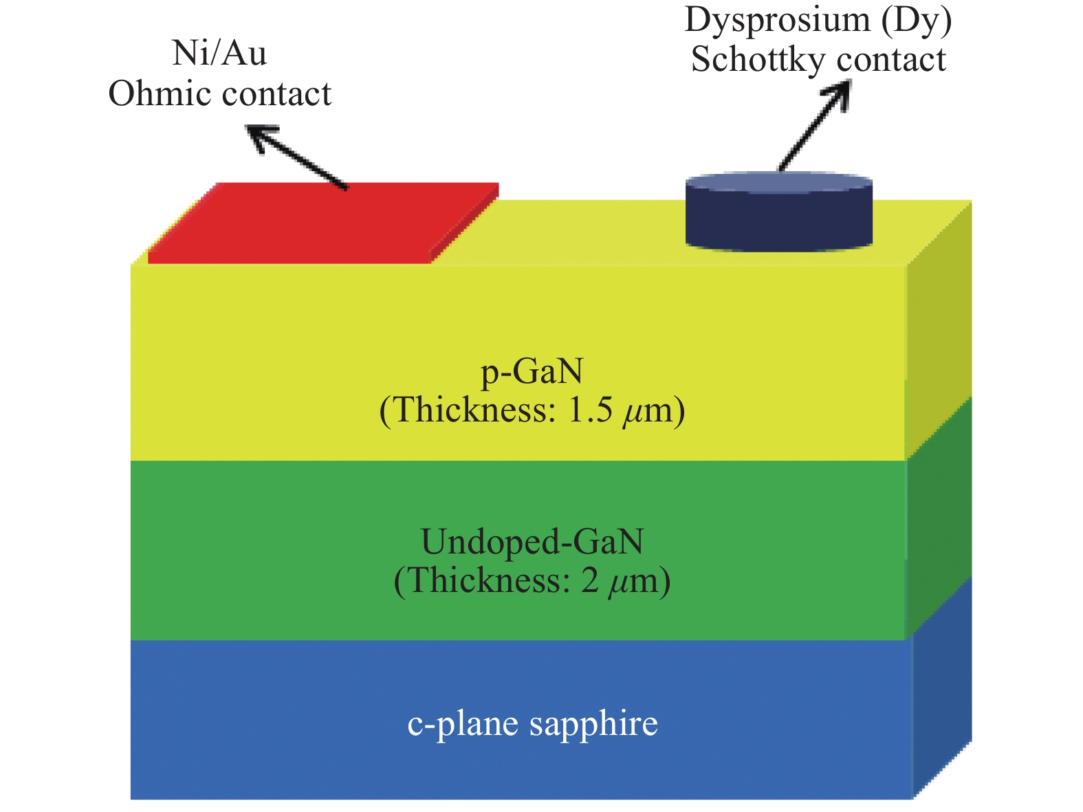
Fig. 1.
(Color online) The schematic structure of a fabricated Dy/p-GaN Schottky barrier diode (SBD).
SEMICONDUCTOR DEVICES
G. Nagaraju1, K. Ravindranatha Reddy2 and V. Rajagopal Reddy1,
Corresponding author: V. Rajagopal Reddy, E-mail: reddy_vrg@rediffmail.com (V.Rajagopal Reddy)
Abstract: The electrical and current transport properties of rapidly annealed Dy/p-GaN SBD are probed by I–V and C–V techniques. The estimated barrier heights (BH) of as-deposited and 200 °C annealed SBDs are 0.80 eV ( I–V)/0.93 eV (C–V) and 0.87 eV (I–V)/1.03 eV (C–V). However, the BH rises to 0.99 eV (I–V)/ 1.18 eV(C–V) and then slightly deceases to 0.92 eV (I–V)/1.03 eV (C–V) after annealing at 300 °C and 400 °C. The utmost BH is attained after annealing at 300 °C and thus the optimum annealing for SBD is 300 °C. By applying Cheung’s functions, the series resistance of the SBD is estimated. The BHs estimated by I–V, Cheung’s and ΨS–V plot are closely matched; hence the techniques used here are consistency and validity. The interface state density of the as-deposited and annealed contacts are calculated and we found that the NSS decreases up to 300 °C annealing and then slightly increases after annealing at 400 °C. Analysis indicates that ohmic and space charge limited conduction mechanisms are found at low and higher voltages in forward-bias irrespective of annealing temperatures. Our experimental results demonstrate that the Poole–Frenkel emission is leading under the reverse bias of Dy/p-GaN SBD at all annealing temperatures.
Keywords: p-GaN, rare-earth Dy Schottky contacts, annealing effects, electrical properties, energy distribution profiles, carrier transport mechanism
| [1] |
Morkoc H, Strite S, Gao G B, et al. Large-band-gap SiC, III--V nitride, and II--VI ZnSe-based semiconductor device technologies. J Appl Phys, 1994, 76(3): 1363 doi: 10.1063/1.358463
|
| [2] |
Jain S C, Willander M, Narayan J, et al. III-nitrides: growth, characterization, and properties. J Appl Phys, 2000, 87(3): 965 doi: 10.1063/1.371971
|
| [3] |
Ambacher O. Growth and applications of group III-nitrides. J Phys D, 1998, 31(20): 2653 doi: 10.1088/0022-3727/31/20/001
|
| [4] |
Moon J. Micovic M, Kurdoghlian A, et al. Microwave noise performance of AlGaN-GaN HEMTs with small DC power dissipation. IEEE Electron Device Lett, 2002, 23 (11): 637 doi: 10.1109/LED.2002.803766
|
| [5] |
Mistele D, Rotter T, Rover K S, et al. First AlGaN/GaN MOSFET with photoanodic gate dielectric. Mater Sci Eng B, 2002, 93(1–3): 107 doi: 10.1016/S0921-5107(02)00052-1
|
| [6] |
Brown J, Borges R, Pinner E, et al. AlGaN/GaN HFETs fabricated on 100-mm GaN on silicon (111) substrates. Solid-State Electron, 2002, 46(10): 1535 doi: 10.1016/S0038-1101(02)00101-6
|
| [7] |
Matioli E, Brinkley S, Kelchner K M, et al. High-brightness polarized light-emitting diodes. Light Sci Appl, 2012, 1(8): e22 doi: 10.1038/lsa.2012.22
|
| [8] |
Wu J. When group-III nitrides go infrared: new properties and perspectives. J Appl Phys, 2009, 106(1): 011101 doi: 10.1063/1.3155798
|
| [9] |
Mori T, Kozawa T, Ohwaki T, et al. Schottky barriers and contact resistances on p-type GaN. Appl Phys Lett, 1996, 69(23): 3537 doi: 10.1063/1.117237
|
| [10] |
Cao X.A, Pearton S J, Dang G, et al. Effects of interfacial oxides on Schottky barrier contacts to n- and p-type GaN. Appl Phys Lett, 1999, 75(26): 4130 doi: 10.1063/1.125559
|
| [11] |
Shiojima K, Sugahara T, Sakai S, et al. Large Schottky barriers for Ni/p-GaN contacts. Appl Phys Lett, 1999, 74(14): 1936 doi: 10.1063/1.123733
|
| [12] |
Hibbard D L, Chuang R W, Zhao Y S, et al. Thermally induced variation in barrier height and ideality factor of Ni/Au contacts to p-GaN. J Electron Mater, 2000, 29(3): 291 doi: 10.1007/s11664-000-0065-9
|
| [13] |
Yu L S, Qiao D, Jia L, et al. Study of Schottky barrier of Ni on P-GaN. Appl Phys Lett, 2001, 79(27): 4536 doi: 10.1063/1.1428773
|
| [14] |
Hartlieb P J, Roskowski A, Davis R F, et al. Pd growth and subsequent Schottky barrier formation on chemical vapor cleaned p-type GaN surfaces. J Appl Phys, 2002, 91(2): 732 doi: 10.1063/1.1424060
|
| [15] |
Tan C K, Aziz A A, Yam F K. Schottky barrier properties of various metal (Zr, Ti, Cr, Pt) contact on p-GaN revealed from I–V–T measurement. Appl Surf Sci, 2006, 252(16): 5930 doi: 10.1016/j.apsusc.2005.08.018
|
| [16] |
Stafford L, Voss L F, Pearton S J, et al. Schottky barrier height of boride-based rectifying contacts to p-GaN. Appl Phys Lett, 2006, 89(13): 132110 doi: 10.1063/1.2357855
|
| [17] |
Fukushima Y, Ogisu K, Kuzuhara M, et al. I–V and C–V characteristics of rare-earth-metal/p-GaN Schottky contacts. Phys Stat Sol C, 2009, 6(S2): S856 doi: 10.1002/pssc.v6.5s2
|
| [18] |
Greco G, Prystawko P, Leszczynski M, et al. Electro-structural evolution and Schottky barrier height in annealed Au/Ni contacts onto p-GaN. J Appl Phys, 2011, 110(12): 123703 doi: 10.1063/1.3669407
|
| [19] |
Choi Y Y, Kim S, Oh M, et al. Investigation of Fermi level pinning at semipolar (11-22) p-type GaN surfaces. Superlattices Microstruct, 2015, 77: 76 doi: 10.1016/j.spmi.2014.10.031
|
| [20] |
Naganawa M, Aoki T, Son J S, et al. Electrical characteristics of a-plane low-Mg-doped p-GaN Schottky contacts. Phys Stat Sol B, 2015, 252(5): 1024 doi: 10.1002/pssb.v252.5
|
| [21] |
Jang S H, Jang J S. Electrical characteristics and carrier transport mechanism for Ti/p-GaN Schottky diodes. Electron Mater Lett, 2013, 9(2): 245 doi: 10.1007/s13391-012-2175-y
|
| [22] |
Nagaraju G, Dasaradha Rao L, Rajagopal Reddy V. Annealing effects on the electrical, structural and morphological properties of Ti/p-GaN/Ni/Au Schottky diode. Appl Phys A, 2015, 12(1): 131
|
| [23] |
Rajagopal Reddy V, Asha B, Choi C J. Effects of annealing on electrical characteristics and current transport mechanisms of the Y/p-GaN Schottky diode. J Electron Mater, 2016, 45(7): 3268 doi: 10.1007/s11664-016-4490-9
|
| [24] |
Jyothi I, Janardhanam V, Kim J H, et al. Electrical and structural properties of Au/Yb Schottky contact on p-type GaN as a function of the annealing temperature. J Alloys Compd, 2016, 688: 875 doi: 10.1016/j.jallcom.2016.07.292
|
| [25] |
Sze S M. Physics of semiconductor devices. 2nd ed. New York: Wiley, 1981
|
| [26] |
Lee K N, Cao X A, Abernathy C R, et al. Effects of thermal stability of GaN epi-layer on the Schottky diodes. Solid-State Electron, 2000, 44(7): 1203 doi: 10.1016/S0038-1101(00)00041-1
|
| [27] |
Rhoderick E H, Williams R H. Metal semiconductor contacts. 2nd ed. Oxford: Clarendon Press, 1988
|
| [28] |
Tung R T. Electron transport at metal –semiconductor interfaces: general theory. Phys Rev B, 1992, 45(23): 13509 doi: 10.1103/PhysRevB.45.13509
|
| [29] |
Crowell C R. The physical significance of the anomalies in Schottky barriers. Solid-State Electron, 1977, 20(3): 171 doi: 10.1016/0038-1101(77)90180-0
|
| [30] |
Cheung S K, Cheung N W. Extraction of Schottky diode parameters from forward current-voltage characteristics. Appl Phys Lett, 1986, 49(2): 85 doi: 10.1063/1.97359
|
| [31] |
Chattopadhyay S, Bera L K, Ray S K, et al. Extraction of interface state density of Pt/p-strained-Si Schottky diode. Thin Solid Films, 1998, 335(1/2): 142
|
| [32] |
Chattopadhyay P. A new technique for the determination of barrier height of Schottky barrier diodes. Solid-State Electron, 1995, 38(3): 739 doi: 10.1016/0038-1101(94)00167-E
|
| [33] |
Bouiadjra W B, Kadaoui M A, Saidane A, et al. Influence of annealing temperature on electrical characteristics of Ti/Au/GaAsN Schottky diode with 0.2% nitrogen incorporation. Mater Sci Semicond Process, 2014, 22: 92 doi: 10.1016/j.mssp.2014.01.041
|
| [34] |
Lien C D, So F C T, Nicolet M A. An improved forward I–V method for nonideal Schottky diodes with high series resistance. IEEE Trans Electron Dev, 1984, 31(10): 1502 doi: 10.1109/T-ED.1984.21739
|
| [35] |
Aubry V, Meyer F. Schottky diodes with high series resistance: limitations of forward I-V methods. J Appl Phys, 1994, 76(12): 7973 doi: 10.1063/1.357909
|
| [36] |
Fontaine C, Okumura T, Tu K N. Interfacial reaction and Schottky barrier between Pt and GaAs. J Appl Phys, 1983, 54(3): 1404 doi: 10.1063/1.332165
|
| [37] |
Song Y P, Van Meirhaeghe R L, Laflere W H, et al. On the difference in apparent barrier height as obtained from capacitance–voltage and current–voltage–temperature measurements on Al/p-InP Schottky barriers. Solid-State Electron, 1986, 29(6): 633 doi: 10.1016/0038-1101(86)90145-0
|
| [38] |
Werner J H, Guttler H. Barrier inhomogeneities at Schottky contacts. J Appl Phys, 1991, 69(3): 1522 doi: 10.1063/1.347243
|
| [39] |
Gullu O, Turut A. Electrical analysis of organic interlayer based metal/interlayer/semiconductor diode structures. J Appl Phys, 2009, 106(10): 103717 doi: 10.1063/1.3261835
|
| [40] |
Card H C, Rhoderick E H. Studies of tunnel MOS diodes I. Interface effects in silicon Schottky diodes. J Phys D, 1971, 4(29): 1589
|
| [41] |
Kolnik J, Ozvold M. The influence of inversion surface layers on the evaluation of the interface state energy distribution from Schottky diode I-V characteristics. Phys Stat Sol A, 1990, 122: 583 doi: 10.1002/(ISSN)1521-396X
|
| [42] |
Kar S, Dahlke W E. Interface states in MOS structures with 20-40 Å thick SiO2 films on nondegenerate Si. Solid-State Electron, 1972, 15(2): 221 doi: 10.1016/0038-1101(72)90056-1
|
| [43] |
Aydogan S, Saglam M, Turut A. The effects of the temperature on the some parameters obtained from current-voltage and capacitance-voltage characteristics of polypyrrole/n-Si structure. Polymer, 2005, 46(2): 563 doi: 10.1016/j.polymer.2004.11.006
|
| [44] |
Forrest S R. Ultrathin organic films grown by organic molecular beam deposition and related techniques. Chem Rev, 1997, 97(6): 1793 doi: 10.1021/cr941014o
|
| [45] |
Yeargan J R, Taylor H L. The Poole-Frenkel effect with compensation present. J Appl Phys, 1968, 39(12): 5600 doi: 10.1063/1.1656022
|
| [46] |
Lee H D. Characterization of shallow silicided junctions for sub-quarter micron ULSI technology-extraction of silicidation induced Schottky contact area. IEEE Trans Electron Devices, 2000, 47(4): 762 doi: 10.1109/16.830991
|
| [47] |
Janardhanam V, Lee H K, Shim K H, et al. Temperature dependency and carrier transport mechanisms of Ti/p-type InP Schottky rectifiers. J Alloys Compd, 2010, 504 (1): 146 doi: 10.1016/j.jallcom.2010.05.074
|
| [48] |
Ashok Kumar A, Rajagopal Reddy V, Janardhanam V, et al. Electrical properties of Pt/n-type Ge Schottky contact with PEDOT: PSS interlayer. J Alloys Compd, 2013, 549: 18 doi: 10.1016/j.jallcom.2012.09.085
|
| [49] |
Rajagopal Reddy V, Janardhanam V, Ju J W, et al. Electrical properties of Au/Bi0.5Na0.5TiO3-BaTiO3/n-GaN metal–insulator–semiconductor (MIS) structure. Semicond Sci Technol, 2014, 29(7): 075001 doi: 10.1088/0268-1242/29/7/075001
|

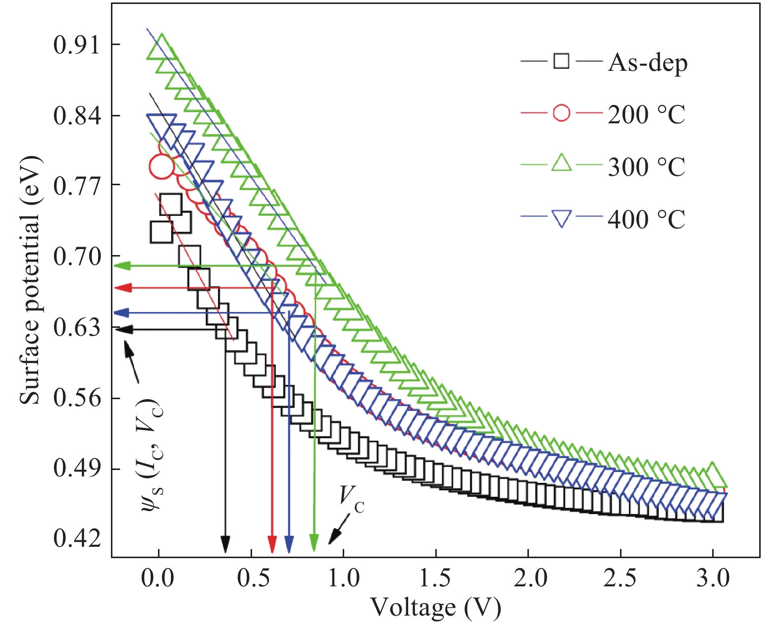
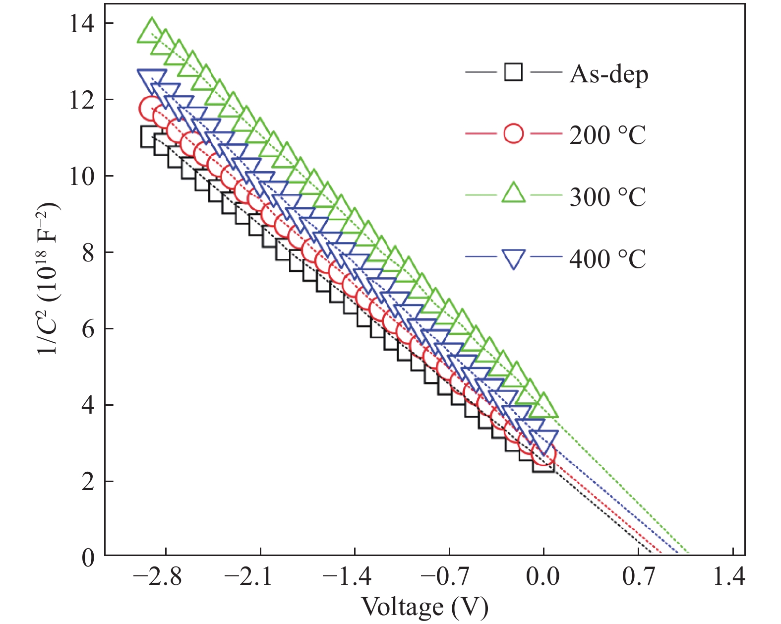
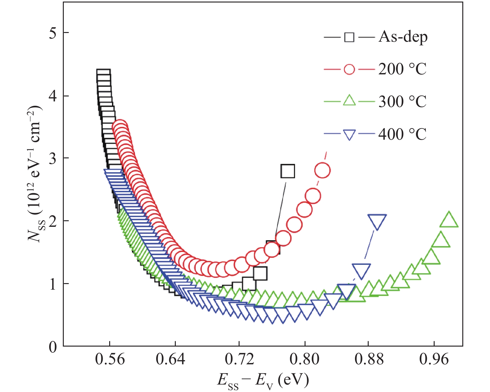
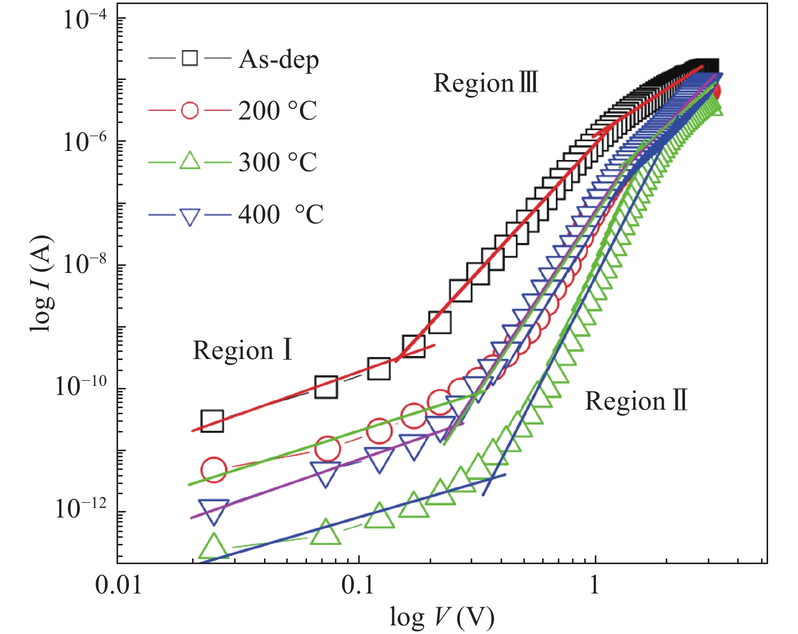

Table 1. The estimated barrier height, ideality factor, series resistance and interface state density of the Dy/p-GaN SBD by I–V and C–V methods as a function of annealing.
| Parameter | As-dep. | 200 °C | 300 °C | 400 °C |
| I–V characteristics | ||||
| Barrier height, Φb (eV) | 0.8 | 0.87 | 0.99 | 0.92 |
| Ideality factor, n | 1.84 | 1.43 | 1.31 | 1.63 |
| Shunt Resistance, RSh (Ω) | 4.26 × 10 8 | 4.33 × 10 9 | 4.70 × 10 11 | 4.17 × 10 10 |
| Series resistance, RS (kΩ) | 142 | 150 | 431 | 132 |
| Cheung’s functions dV/d(ln I) versus I | ||||
| Series resistance, RS (kΩ) | 169 | 403 | 492 | 427 |
| Ideality factor, n | 2.81 | 2.46 | 2.32 | 2.63 |
| H(I) versus I | ||||
| Series resistance, RS (kΩ) | 201 | 461 | 613 | 501 |
| Barrier height, Φb (eV) | 0.83 | 0.93 | 0.98 | 0.91 |
| C–V characteristics | ||||
| Barrier height, Φb (eV) | 0.93 | 1.03 | 1.18 | 1.13 |
| Built-in potential (V) | 0.83 | 0.93 | 1.08 | 1.03 |
| Interface state density (NSS) | 2.8(0.77 eV–Ev) to | 2.81(0.82 eV–Ev) to | 1.99(0.98 eV–Ev) to | 2.02(0.89 eV–Ev) to |
| ranges (1012 cm–2 eV–1) | 4.32(0.54 eV–Ev) | 3.51(0.57 eV–Ev) | to 2.27(0.58 eV–Ev) | 2.75(0.56 eV–Ev) |
 DownLoad: CSV
Table 2. The theoretical and experimental slope values of Poole-Frenkel emission and Schottky emission for the Dy/p-type GaN SBD as a function of annealing.
| Sample | Poole-Frenkel emission | Schottky emission | |||
| Theoretical | Experimental | Theoretical | Experimental | ||
| As-dep | 0.0208 | 0.0234 | |||
| 200 °C | 0.00951 | 0.0282 | 0.00475 | 0.0308 | |
| 300 °C | 0.038 | 0.0408 | |||
| 400 °C | 0.0324 | 0.0352 | |||
DownLoad: CSV
| [1] |
Morkoc H, Strite S, Gao G B, et al. Large-band-gap SiC, III--V nitride, and II--VI ZnSe-based semiconductor device technologies. J Appl Phys, 1994, 76(3): 1363 doi: 10.1063/1.358463
|
| [2] |
Jain S C, Willander M, Narayan J, et al. III-nitrides: growth, characterization, and properties. J Appl Phys, 2000, 87(3): 965 doi: 10.1063/1.371971
|
| [3] |
Ambacher O. Growth and applications of group III-nitrides. J Phys D, 1998, 31(20): 2653 doi: 10.1088/0022-3727/31/20/001
|
| [4] |
Moon J. Micovic M, Kurdoghlian A, et al. Microwave noise performance of AlGaN-GaN HEMTs with small DC power dissipation. IEEE Electron Device Lett, 2002, 23 (11): 637 doi: 10.1109/LED.2002.803766
|
| [5] |
Mistele D, Rotter T, Rover K S, et al. First AlGaN/GaN MOSFET with photoanodic gate dielectric. Mater Sci Eng B, 2002, 93(1–3): 107 doi: 10.1016/S0921-5107(02)00052-1
|
| [6] |
Brown J, Borges R, Pinner E, et al. AlGaN/GaN HFETs fabricated on 100-mm GaN on silicon (111) substrates. Solid-State Electron, 2002, 46(10): 1535 doi: 10.1016/S0038-1101(02)00101-6
|
| [7] |
Matioli E, Brinkley S, Kelchner K M, et al. High-brightness polarized light-emitting diodes. Light Sci Appl, 2012, 1(8): e22 doi: 10.1038/lsa.2012.22
|
| [8] |
Wu J. When group-III nitrides go infrared: new properties and perspectives. J Appl Phys, 2009, 106(1): 011101 doi: 10.1063/1.3155798
|
| [9] |
Mori T, Kozawa T, Ohwaki T, et al. Schottky barriers and contact resistances on p-type GaN. Appl Phys Lett, 1996, 69(23): 3537 doi: 10.1063/1.117237
|
| [10] |
Cao X.A, Pearton S J, Dang G, et al. Effects of interfacial oxides on Schottky barrier contacts to n- and p-type GaN. Appl Phys Lett, 1999, 75(26): 4130 doi: 10.1063/1.125559
|
| [11] |
Shiojima K, Sugahara T, Sakai S, et al. Large Schottky barriers for Ni/p-GaN contacts. Appl Phys Lett, 1999, 74(14): 1936 doi: 10.1063/1.123733
|
| [12] |
Hibbard D L, Chuang R W, Zhao Y S, et al. Thermally induced variation in barrier height and ideality factor of Ni/Au contacts to p-GaN. J Electron Mater, 2000, 29(3): 291 doi: 10.1007/s11664-000-0065-9
|
| [13] |
Yu L S, Qiao D, Jia L, et al. Study of Schottky barrier of Ni on P-GaN. Appl Phys Lett, 2001, 79(27): 4536 doi: 10.1063/1.1428773
|
| [14] |
Hartlieb P J, Roskowski A, Davis R F, et al. Pd growth and subsequent Schottky barrier formation on chemical vapor cleaned p-type GaN surfaces. J Appl Phys, 2002, 91(2): 732 doi: 10.1063/1.1424060
|
| [15] |
Tan C K, Aziz A A, Yam F K. Schottky barrier properties of various metal (Zr, Ti, Cr, Pt) contact on p-GaN revealed from I–V–T measurement. Appl Surf Sci, 2006, 252(16): 5930 doi: 10.1016/j.apsusc.2005.08.018
|
| [16] |
Stafford L, Voss L F, Pearton S J, et al. Schottky barrier height of boride-based rectifying contacts to p-GaN. Appl Phys Lett, 2006, 89(13): 132110 doi: 10.1063/1.2357855
|
| [17] |
Fukushima Y, Ogisu K, Kuzuhara M, et al. I–V and C–V characteristics of rare-earth-metal/p-GaN Schottky contacts. Phys Stat Sol C, 2009, 6(S2): S856 doi: 10.1002/pssc.v6.5s2
|
| [18] |
Greco G, Prystawko P, Leszczynski M, et al. Electro-structural evolution and Schottky barrier height in annealed Au/Ni contacts onto p-GaN. J Appl Phys, 2011, 110(12): 123703 doi: 10.1063/1.3669407
|
| [19] |
Choi Y Y, Kim S, Oh M, et al. Investigation of Fermi level pinning at semipolar (11-22) p-type GaN surfaces. Superlattices Microstruct, 2015, 77: 76 doi: 10.1016/j.spmi.2014.10.031
|
| [20] |
Naganawa M, Aoki T, Son J S, et al. Electrical characteristics of a-plane low-Mg-doped p-GaN Schottky contacts. Phys Stat Sol B, 2015, 252(5): 1024 doi: 10.1002/pssb.v252.5
|
| [21] |
Jang S H, Jang J S. Electrical characteristics and carrier transport mechanism for Ti/p-GaN Schottky diodes. Electron Mater Lett, 2013, 9(2): 245 doi: 10.1007/s13391-012-2175-y
|
| [22] |
Nagaraju G, Dasaradha Rao L, Rajagopal Reddy V. Annealing effects on the electrical, structural and morphological properties of Ti/p-GaN/Ni/Au Schottky diode. Appl Phys A, 2015, 12(1): 131
|
| [23] |
Rajagopal Reddy V, Asha B, Choi C J. Effects of annealing on electrical characteristics and current transport mechanisms of the Y/p-GaN Schottky diode. J Electron Mater, 2016, 45(7): 3268 doi: 10.1007/s11664-016-4490-9
|
| [24] |
Jyothi I, Janardhanam V, Kim J H, et al. Electrical and structural properties of Au/Yb Schottky contact on p-type GaN as a function of the annealing temperature. J Alloys Compd, 2016, 688: 875 doi: 10.1016/j.jallcom.2016.07.292
|
| [25] |
Sze S M. Physics of semiconductor devices. 2nd ed. New York: Wiley, 1981
|
| [26] |
Lee K N, Cao X A, Abernathy C R, et al. Effects of thermal stability of GaN epi-layer on the Schottky diodes. Solid-State Electron, 2000, 44(7): 1203 doi: 10.1016/S0038-1101(00)00041-1
|
| [27] |
Rhoderick E H, Williams R H. Metal semiconductor contacts. 2nd ed. Oxford: Clarendon Press, 1988
|
| [28] |
Tung R T. Electron transport at metal –semiconductor interfaces: general theory. Phys Rev B, 1992, 45(23): 13509 doi: 10.1103/PhysRevB.45.13509
|
| [29] |
Crowell C R. The physical significance of the anomalies in Schottky barriers. Solid-State Electron, 1977, 20(3): 171 doi: 10.1016/0038-1101(77)90180-0
|
| [30] |
Cheung S K, Cheung N W. Extraction of Schottky diode parameters from forward current-voltage characteristics. Appl Phys Lett, 1986, 49(2): 85 doi: 10.1063/1.97359
|
| [31] |
Chattopadhyay S, Bera L K, Ray S K, et al. Extraction of interface state density of Pt/p-strained-Si Schottky diode. Thin Solid Films, 1998, 335(1/2): 142
|
| [32] |
Chattopadhyay P. A new technique for the determination of barrier height of Schottky barrier diodes. Solid-State Electron, 1995, 38(3): 739 doi: 10.1016/0038-1101(94)00167-E
|
| [33] |
Bouiadjra W B, Kadaoui M A, Saidane A, et al. Influence of annealing temperature on electrical characteristics of Ti/Au/GaAsN Schottky diode with 0.2% nitrogen incorporation. Mater Sci Semicond Process, 2014, 22: 92 doi: 10.1016/j.mssp.2014.01.041
|
| [34] |
Lien C D, So F C T, Nicolet M A. An improved forward I–V method for nonideal Schottky diodes with high series resistance. IEEE Trans Electron Dev, 1984, 31(10): 1502 doi: 10.1109/T-ED.1984.21739
|
| [35] |
Aubry V, Meyer F. Schottky diodes with high series resistance: limitations of forward I-V methods. J Appl Phys, 1994, 76(12): 7973 doi: 10.1063/1.357909
|
| [36] |
Fontaine C, Okumura T, Tu K N. Interfacial reaction and Schottky barrier between Pt and GaAs. J Appl Phys, 1983, 54(3): 1404 doi: 10.1063/1.332165
|
| [37] |
Song Y P, Van Meirhaeghe R L, Laflere W H, et al. On the difference in apparent barrier height as obtained from capacitance–voltage and current–voltage–temperature measurements on Al/p-InP Schottky barriers. Solid-State Electron, 1986, 29(6): 633 doi: 10.1016/0038-1101(86)90145-0
|
| [38] |
Werner J H, Guttler H. Barrier inhomogeneities at Schottky contacts. J Appl Phys, 1991, 69(3): 1522 doi: 10.1063/1.347243
|
| [39] |
Gullu O, Turut A. Electrical analysis of organic interlayer based metal/interlayer/semiconductor diode structures. J Appl Phys, 2009, 106(10): 103717 doi: 10.1063/1.3261835
|
| [40] |
Card H C, Rhoderick E H. Studies of tunnel MOS diodes I. Interface effects in silicon Schottky diodes. J Phys D, 1971, 4(29): 1589
|
| [41] |
Kolnik J, Ozvold M. The influence of inversion surface layers on the evaluation of the interface state energy distribution from Schottky diode I-V characteristics. Phys Stat Sol A, 1990, 122: 583 doi: 10.1002/(ISSN)1521-396X
|
| [42] |
Kar S, Dahlke W E. Interface states in MOS structures with 20-40 Å thick SiO2 films on nondegenerate Si. Solid-State Electron, 1972, 15(2): 221 doi: 10.1016/0038-1101(72)90056-1
|
| [43] |
Aydogan S, Saglam M, Turut A. The effects of the temperature on the some parameters obtained from current-voltage and capacitance-voltage characteristics of polypyrrole/n-Si structure. Polymer, 2005, 46(2): 563 doi: 10.1016/j.polymer.2004.11.006
|
| [44] |
Forrest S R. Ultrathin organic films grown by organic molecular beam deposition and related techniques. Chem Rev, 1997, 97(6): 1793 doi: 10.1021/cr941014o
|
| [45] |
Yeargan J R, Taylor H L. The Poole-Frenkel effect with compensation present. J Appl Phys, 1968, 39(12): 5600 doi: 10.1063/1.1656022
|
| [46] |
Lee H D. Characterization of shallow silicided junctions for sub-quarter micron ULSI technology-extraction of silicidation induced Schottky contact area. IEEE Trans Electron Devices, 2000, 47(4): 762 doi: 10.1109/16.830991
|
| [47] |
Janardhanam V, Lee H K, Shim K H, et al. Temperature dependency and carrier transport mechanisms of Ti/p-type InP Schottky rectifiers. J Alloys Compd, 2010, 504 (1): 146 doi: 10.1016/j.jallcom.2010.05.074
|
| [48] |
Ashok Kumar A, Rajagopal Reddy V, Janardhanam V, et al. Electrical properties of Pt/n-type Ge Schottky contact with PEDOT: PSS interlayer. J Alloys Compd, 2013, 549: 18 doi: 10.1016/j.jallcom.2012.09.085
|
| [49] |
Rajagopal Reddy V, Janardhanam V, Ju J W, et al. Electrical properties of Au/Bi0.5Na0.5TiO3-BaTiO3/n-GaN metal–insulator–semiconductor (MIS) structure. Semicond Sci Technol, 2014, 29(7): 075001 doi: 10.1088/0268-1242/29/7/075001
|


Article views: 4822 Times PDF downloads: 61 Times Cited by: 0 Times
Received: 27 January 2017 Revised: 04 May 2017 Online: Uncorrected proof: 30 October 2017Accepted Manuscript: 13 November 2017Published: 01 November 2017
| Citation: |
G. Nagaraju, K. Ravindranatha Reddy, V. Rajagopal Reddy. Electrical transport and current properties of rare-earth dysprosium Schottky electrode on p-type GaN at various annealing temperatures[J]. Journal of Semiconductors, 2017, 38(11): 114001. doi: 10.1088/1674-4926/38/11/114001
****
G. Nagaraju, K. R. Reddy, V. R. Reddy. Electrical transport and current properties of rare-earth dysprosium Schottky electrode on p-type GaN at various annealing temperatures[J]. J. Semicond., 2017, 38(11): 114001. doi: 10.1088/1674-4926/38/11/114001.

|
| [1] |
Morkoc H, Strite S, Gao G B, et al. Large-band-gap SiC, III--V nitride, and II--VI ZnSe-based semiconductor device technologies. J Appl Phys, 1994, 76(3): 1363 doi: 10.1063/1.358463
|
| [2] |
Jain S C, Willander M, Narayan J, et al. III-nitrides: growth, characterization, and properties. J Appl Phys, 2000, 87(3): 965 doi: 10.1063/1.371971
|
| [3] |
Ambacher O. Growth and applications of group III-nitrides. J Phys D, 1998, 31(20): 2653 doi: 10.1088/0022-3727/31/20/001
|
| [4] |
Moon J. Micovic M, Kurdoghlian A, et al. Microwave noise performance of AlGaN-GaN HEMTs with small DC power dissipation. IEEE Electron Device Lett, 2002, 23 (11): 637 doi: 10.1109/LED.2002.803766
|
| [5] |
Mistele D, Rotter T, Rover K S, et al. First AlGaN/GaN MOSFET with photoanodic gate dielectric. Mater Sci Eng B, 2002, 93(1–3): 107 doi: 10.1016/S0921-5107(02)00052-1
|
| [6] |
Brown J, Borges R, Pinner E, et al. AlGaN/GaN HFETs fabricated on 100-mm GaN on silicon (111) substrates. Solid-State Electron, 2002, 46(10): 1535 doi: 10.1016/S0038-1101(02)00101-6
|
| [7] |
Matioli E, Brinkley S, Kelchner K M, et al. High-brightness polarized light-emitting diodes. Light Sci Appl, 2012, 1(8): e22 doi: 10.1038/lsa.2012.22
|
| [8] |
Wu J. When group-III nitrides go infrared: new properties and perspectives. J Appl Phys, 2009, 106(1): 011101 doi: 10.1063/1.3155798
|
| [9] |
Mori T, Kozawa T, Ohwaki T, et al. Schottky barriers and contact resistances on p-type GaN. Appl Phys Lett, 1996, 69(23): 3537 doi: 10.1063/1.117237
|
| [10] |
Cao X.A, Pearton S J, Dang G, et al. Effects of interfacial oxides on Schottky barrier contacts to n- and p-type GaN. Appl Phys Lett, 1999, 75(26): 4130 doi: 10.1063/1.125559
|
| [11] |
Shiojima K, Sugahara T, Sakai S, et al. Large Schottky barriers for Ni/p-GaN contacts. Appl Phys Lett, 1999, 74(14): 1936 doi: 10.1063/1.123733
|
| [12] |
Hibbard D L, Chuang R W, Zhao Y S, et al. Thermally induced variation in barrier height and ideality factor of Ni/Au contacts to p-GaN. J Electron Mater, 2000, 29(3): 291 doi: 10.1007/s11664-000-0065-9
|
| [13] |
Yu L S, Qiao D, Jia L, et al. Study of Schottky barrier of Ni on P-GaN. Appl Phys Lett, 2001, 79(27): 4536 doi: 10.1063/1.1428773
|
| [14] |
Hartlieb P J, Roskowski A, Davis R F, et al. Pd growth and subsequent Schottky barrier formation on chemical vapor cleaned p-type GaN surfaces. J Appl Phys, 2002, 91(2): 732 doi: 10.1063/1.1424060
|
| [15] |
Tan C K, Aziz A A, Yam F K. Schottky barrier properties of various metal (Zr, Ti, Cr, Pt) contact on p-GaN revealed from I–V–T measurement. Appl Surf Sci, 2006, 252(16): 5930 doi: 10.1016/j.apsusc.2005.08.018
|
| [16] |
Stafford L, Voss L F, Pearton S J, et al. Schottky barrier height of boride-based rectifying contacts to p-GaN. Appl Phys Lett, 2006, 89(13): 132110 doi: 10.1063/1.2357855
|
| [17] |
Fukushima Y, Ogisu K, Kuzuhara M, et al. I–V and C–V characteristics of rare-earth-metal/p-GaN Schottky contacts. Phys Stat Sol C, 2009, 6(S2): S856 doi: 10.1002/pssc.v6.5s2
|
| [18] |
Greco G, Prystawko P, Leszczynski M, et al. Electro-structural evolution and Schottky barrier height in annealed Au/Ni contacts onto p-GaN. J Appl Phys, 2011, 110(12): 123703 doi: 10.1063/1.3669407
|
| [19] |
Choi Y Y, Kim S, Oh M, et al. Investigation of Fermi level pinning at semipolar (11-22) p-type GaN surfaces. Superlattices Microstruct, 2015, 77: 76 doi: 10.1016/j.spmi.2014.10.031
|
| [20] |
Naganawa M, Aoki T, Son J S, et al. Electrical characteristics of a-plane low-Mg-doped p-GaN Schottky contacts. Phys Stat Sol B, 2015, 252(5): 1024 doi: 10.1002/pssb.v252.5
|
| [21] |
Jang S H, Jang J S. Electrical characteristics and carrier transport mechanism for Ti/p-GaN Schottky diodes. Electron Mater Lett, 2013, 9(2): 245 doi: 10.1007/s13391-012-2175-y
|
| [22] |
Nagaraju G, Dasaradha Rao L, Rajagopal Reddy V. Annealing effects on the electrical, structural and morphological properties of Ti/p-GaN/Ni/Au Schottky diode. Appl Phys A, 2015, 12(1): 131
|
| [23] |
Rajagopal Reddy V, Asha B, Choi C J. Effects of annealing on electrical characteristics and current transport mechanisms of the Y/p-GaN Schottky diode. J Electron Mater, 2016, 45(7): 3268 doi: 10.1007/s11664-016-4490-9
|
| [24] |
Jyothi I, Janardhanam V, Kim J H, et al. Electrical and structural properties of Au/Yb Schottky contact on p-type GaN as a function of the annealing temperature. J Alloys Compd, 2016, 688: 875 doi: 10.1016/j.jallcom.2016.07.292
|
| [25] |
Sze S M. Physics of semiconductor devices. 2nd ed. New York: Wiley, 1981
|
| [26] |
Lee K N, Cao X A, Abernathy C R, et al. Effects of thermal stability of GaN epi-layer on the Schottky diodes. Solid-State Electron, 2000, 44(7): 1203 doi: 10.1016/S0038-1101(00)00041-1
|
| [27] |
Rhoderick E H, Williams R H. Metal semiconductor contacts. 2nd ed. Oxford: Clarendon Press, 1988
|
| [28] |
Tung R T. Electron transport at metal –semiconductor interfaces: general theory. Phys Rev B, 1992, 45(23): 13509 doi: 10.1103/PhysRevB.45.13509
|
| [29] |
Crowell C R. The physical significance of the anomalies in Schottky barriers. Solid-State Electron, 1977, 20(3): 171 doi: 10.1016/0038-1101(77)90180-0
|
| [30] |
Cheung S K, Cheung N W. Extraction of Schottky diode parameters from forward current-voltage characteristics. Appl Phys Lett, 1986, 49(2): 85 doi: 10.1063/1.97359
|
| [31] |
Chattopadhyay S, Bera L K, Ray S K, et al. Extraction of interface state density of Pt/p-strained-Si Schottky diode. Thin Solid Films, 1998, 335(1/2): 142
|
| [32] |
Chattopadhyay P. A new technique for the determination of barrier height of Schottky barrier diodes. Solid-State Electron, 1995, 38(3): 739 doi: 10.1016/0038-1101(94)00167-E
|
| [33] |
Bouiadjra W B, Kadaoui M A, Saidane A, et al. Influence of annealing temperature on electrical characteristics of Ti/Au/GaAsN Schottky diode with 0.2% nitrogen incorporation. Mater Sci Semicond Process, 2014, 22: 92 doi: 10.1016/j.mssp.2014.01.041
|
| [34] |
Lien C D, So F C T, Nicolet M A. An improved forward I–V method for nonideal Schottky diodes with high series resistance. IEEE Trans Electron Dev, 1984, 31(10): 1502 doi: 10.1109/T-ED.1984.21739
|
| [35] |
Aubry V, Meyer F. Schottky diodes with high series resistance: limitations of forward I-V methods. J Appl Phys, 1994, 76(12): 7973 doi: 10.1063/1.357909
|
| [36] |
Fontaine C, Okumura T, Tu K N. Interfacial reaction and Schottky barrier between Pt and GaAs. J Appl Phys, 1983, 54(3): 1404 doi: 10.1063/1.332165
|
| [37] |
Song Y P, Van Meirhaeghe R L, Laflere W H, et al. On the difference in apparent barrier height as obtained from capacitance–voltage and current–voltage–temperature measurements on Al/p-InP Schottky barriers. Solid-State Electron, 1986, 29(6): 633 doi: 10.1016/0038-1101(86)90145-0
|
| [38] |
Werner J H, Guttler H. Barrier inhomogeneities at Schottky contacts. J Appl Phys, 1991, 69(3): 1522 doi: 10.1063/1.347243
|
| [39] |
Gullu O, Turut A. Electrical analysis of organic interlayer based metal/interlayer/semiconductor diode structures. J Appl Phys, 2009, 106(10): 103717 doi: 10.1063/1.3261835
|
| [40] |
Card H C, Rhoderick E H. Studies of tunnel MOS diodes I. Interface effects in silicon Schottky diodes. J Phys D, 1971, 4(29): 1589
|
| [41] |
Kolnik J, Ozvold M. The influence of inversion surface layers on the evaluation of the interface state energy distribution from Schottky diode I-V characteristics. Phys Stat Sol A, 1990, 122: 583 doi: 10.1002/(ISSN)1521-396X
|
| [42] |
Kar S, Dahlke W E. Interface states in MOS structures with 20-40 Å thick SiO2 films on nondegenerate Si. Solid-State Electron, 1972, 15(2): 221 doi: 10.1016/0038-1101(72)90056-1
|
| [43] |
Aydogan S, Saglam M, Turut A. The effects of the temperature on the some parameters obtained from current-voltage and capacitance-voltage characteristics of polypyrrole/n-Si structure. Polymer, 2005, 46(2): 563 doi: 10.1016/j.polymer.2004.11.006
|
| [44] |
Forrest S R. Ultrathin organic films grown by organic molecular beam deposition and related techniques. Chem Rev, 1997, 97(6): 1793 doi: 10.1021/cr941014o
|
| [45] |
Yeargan J R, Taylor H L. The Poole-Frenkel effect with compensation present. J Appl Phys, 1968, 39(12): 5600 doi: 10.1063/1.1656022
|
| [46] |
Lee H D. Characterization of shallow silicided junctions for sub-quarter micron ULSI technology-extraction of silicidation induced Schottky contact area. IEEE Trans Electron Devices, 2000, 47(4): 762 doi: 10.1109/16.830991
|
| [47] |
Janardhanam V, Lee H K, Shim K H, et al. Temperature dependency and carrier transport mechanisms of Ti/p-type InP Schottky rectifiers. J Alloys Compd, 2010, 504 (1): 146 doi: 10.1016/j.jallcom.2010.05.074
|
| [48] |
Ashok Kumar A, Rajagopal Reddy V, Janardhanam V, et al. Electrical properties of Pt/n-type Ge Schottky contact with PEDOT: PSS interlayer. J Alloys Compd, 2013, 549: 18 doi: 10.1016/j.jallcom.2012.09.085
|
| [49] |
Rajagopal Reddy V, Janardhanam V, Ju J W, et al. Electrical properties of Au/Bi0.5Na0.5TiO3-BaTiO3/n-GaN metal–insulator–semiconductor (MIS) structure. Semicond Sci Technol, 2014, 29(7): 075001 doi: 10.1088/0268-1242/29/7/075001
|

 WeChat ID
Journal of Semiconductors © 2017 All Rights Reserved 京ICP备05085259号-2


