


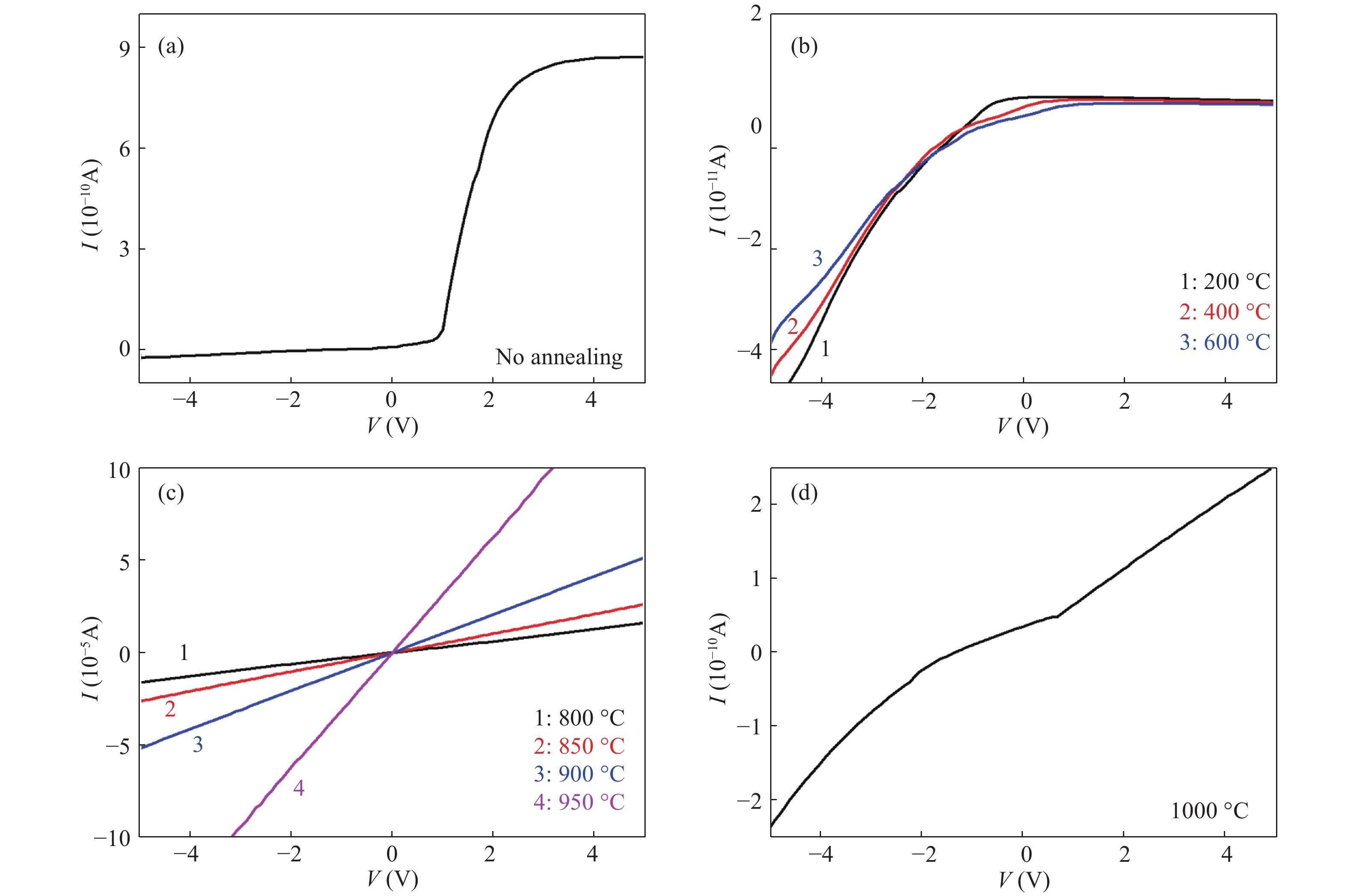
Fig. 1.
(Color online) I–V characteristics of Ti/Al/Ni/Au contacts (CTLM gap = 5 μm) on AlN films (a) before annealing, (b) annealed at 200–600 °C for 2 min, (c) annealed at 800–950 °C for 30 s, (d) annealed at 1000 °C for 30 s.
SEMICONDUCTOR TECHNOLOGY
Xuewei Li1, 3, Jicai Zhang1, 2, Maosong Sun1, Binbin Ye1, 3, Jun Huang1, Zhenyi Xu1, 3, Wenxiu Dong1, Jianfeng Wang1, 2 and Ke Xu1, 2
Corresponding author: Emiail: jczhang2010@sinano.ac.cn, kxu@sinano.ac.cn
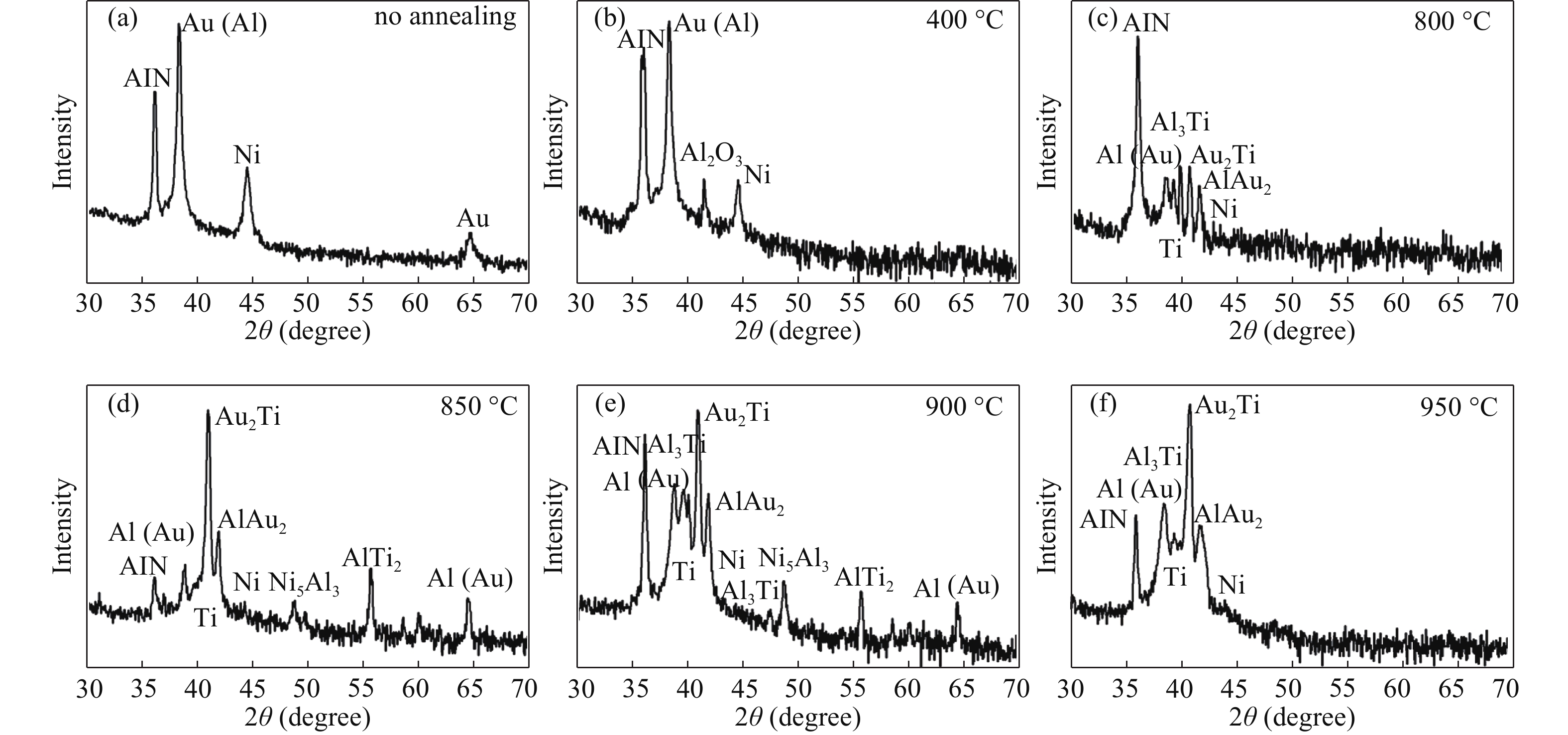
Abstract: The Ti/Al/Ni/Au metals were deposited on undoped AlN films by electron beam evaporation. The influence of annealing temperature on the properties of contacts was investigated. When the annealing temperatures were between 800 and 950 °C, the AlN–Ti/Al/Ni/Au contacts became ohmic contacts and the resistance decreased with the increase of annealing temperature. A lowest specific contacts resistance of 0.379 Ω·cm 2 was obtained for the sample annealed at 950 °C. In this work, we confirmed that the formation mechanism of ohmic contacts on AlN was due to the formation of Al–Au, Au–Ti and Al–Ni alloys, and reduction of the specific contacts resistance could originate from the formation of Au 2Ti and AlAu2 alloys. This result provided a possibility for the preparation of AlN-based high-frequency, high-power devices and deep ultraviolet devices.
Keywords: ohmic contacts, AlN, annealing temperature, Ti/Al/Ni/Au
| [1] |
Hirayama H, Yatabe T, Noguchi N, et al. 231–261 nm AlGaN deep-ultraviolet light-emitting diodes fabricated on AlN multilayer buffers grown by ammonia pulse-flow method on sapphire. Appl Phys Lett, 2007, 91(7): 071901 doi: 10.1063/1.2770662
|
| [2] |
Li D B, Sun X J, Song H, et al. Realization of a High-Performance GaN UV Detector by Nanoplasmonic Enhancement. Adv Mater, 2012, 24(6): 845 doi: 10.1002/adma.201102585
|
| [3] |
Li X, Zhao D G, Jiang D S, et al. Suppression of electron leakage in 808 nm laser diodes with asymmetric waveguide layer. J Semicond, 2016, 37(1): 014007 doi: 10.1088/1674-4926/37/1/014007
|
| [4] |
Zhao D G, Zhang S, Jiang D S, et al. A study on the spectral response of back-illuminated p-i-n AlGaN heterojunction ultraviolet photodetector. J Appl Phys, 2011, 110(5): 053701 doi: 10.1063/1.3629987
|
| [5] |
Miyake H, Lin C H, Tokoro K, et al. Preparation of high-quality AlN on sapphire by high-temperature face-to-face annealing. J Cryst Growth, 2016, 456: 155 doi: 10.1016/j.jcrysgro.2016.08.028
|
| [6] |
Kinoshita T, Hironaka K, Obata To, et al. Deep-Ultraviolet Light-Emitting Diodes Fabricated on AlN Substrates Prepared by Hydride Vapor Phase Epitaxy. Appl Phys Express, 2012, 5(12): 122101 doi: 10.1143/APEX.5.122101
|
| [7] |
Zhao S, Connie A T, Dastjerdi M H, et al. Aluminum nitride nanowire light emitting diodes: Breaking the fundamental bottleneck of deep ultraviolet light sources. Sci Rep, 2015, 5: 8332 doi: 10.1038/srep08332
|
| [8] |
Feng Q, Li L M, Hao Y, et al. The improvement of ohmic contact of Ti/Al/Ni/Au to AlGaN/GaN HEMT by multi-step annealing method. Solid-State Electron, 2009, 53(9): 955 doi: 10.1016/j.sse.2009.06.002
|
| [9] |
Gu G S, Dun S B, Lü Y J, et al. Low ohmic contact AlN/GaN HEMTs grown by MOCVD. J Semicond, 2013, 34(11): 114004 doi: 10.1088/1674-4926/34/11/114004
|
| [10] |
Zhu Y X, Cao W W, Fan Y Y, et al. Effects of rapid thermal annealing on ohmic contact of AlGaN/GaN HEMTs. J Semicond, 2014, 35(2): 026004 doi: 10.1088/1674-4926/35/2/026004
|
| [11] |
Sachenko A V, Belyaev A E, Boltovets N S, et al. Resistance formation mechanisms for contacts to n-GaN and n-AlN with high dislocation density. Phys Status Solidi C, 2013, 10(3): 498 doi: 10.1002/pssc.201200530
|
| [12] |
Sun M S, Zhang J C, Huang J, et al. Influence of thickness on strain state and surface morphology of AlN grown by HVPE. J Semicond, 2016, 37(12): 123001 doi: 10.1088/1674-4926/37/12/123001
|
| [13] |
Xu C, Wang J Y, Wang M J, et al. Reeves's circular transmission line model and its scope of application to extract specific contact resistance. Solid-State Electron, 2006, 50(5): 843 doi: 10.1016/j.sse.2006.03.007
|
| [14] |
Bright A N, Thomas P J, Weyland M, et al. Correlation of contact resistance with microstructure for Au/Ni/Al/Ti/AlGaN/GaN ohmic contacts using transmission electron microscopy. J Appl Phys, 2001, 89(6): 3143 doi: 10.1063/1.1347003
|
| [15] |
Macherzyński W, Indykiewicz K, Bogdan P. Chemical analysis of Ti/Al/Ni/Au ohmic contacts to AlGaN/GaN heterostructures. Optica Applicata, 2013, 43(1): 67
|
| [16] |
Iucolano F, Greco G, Roccaforte F. Correlation between microstructure and temperature dependent electrical behavior of annealed Ti/Al/Ni/Au ohmic contacts to AlGaN/GaN heterostructures. Appl Phys Lett, 2013, 103(20): 201604 doi: 10.1063/1.4828839
|
| [17] |
Ruvimov S, Liliental-Weber Z, Washburn J, et al. Microstructure of Ti/Al and Ti/Al/Ni/Au Ohmic contacts for n-GaN. Appl Phys Lett, 1996, 69(11): 1556 doi: 10.1063/1.117060
|
| [18] |
Constant A, Baele J, Coppens P, et al. Impact of Ti/Al atomic ratio on the formation mechanism of non-recessed Au-free Ohmic contacts on AlGaN/GaN heterostructures. J Appl Phys, 2016, 120(10): 104502 doi: 10.1063/1.4962314
|
| [19] |
Han C, Zhang Y M, Song Q W, et al. Interface annealing characterization of Ti/Al/Au ohmic contacts to p-type 4h-SiC. J Semicond, 2015, 36(12): 123006 doi: 10.1088/1674-4926/36/12/123006
|
| [20] |
Mahajan S S, Dhaul A, Laishram R, et al. Micro-structural evaluation of Ti/Al/Ni/Au ohmic contacts with different Ti/Al thicknesses in AlGaN/GaN HEMTs. Mater Sci Eng B, 2014, 183: 47 doi: 10.1016/j.mseb.2013.12.005
|
| [21] |
Zhou H M, Shen B, Chen D J, et al. Ti/Al/Ni/Au and Ti/Al/Pt/Au Multi-Layer Ohmic Contacts on AtxGal1-xN/GaN Heterostructures. Chin J Rare Metals, 2004, 28(3): 487
|
| [22] |
Sheremet V N. Formation peculiarities and properties of ohmic contacts to n-GaN(AlN) and artificial diamond. Radioelectron Commun Syst, 2013, 56(10): 493 doi: 10.3103/S073527271310004X
|


Article views: 6032 Times PDF downloads: 194 Times Cited by: 0 Times
Received: 22 April 2017 Revised: 04 May 2017 Online: Uncorrected proof: 30 October 2017Accepted Manuscript: 13 November 2017Published: 01 November 2017
| Citation: |
Xuewei Li, Jicai Zhang, Maosong Sun, Binbin Ye, Jun Huang, Zhenyi Xu, Wenxiu Dong, Jianfeng Wang, Ke Xu. Effect of annealing temperature on Ti/Al/Ni/Au ohmic contacts on undoped AlN films[J]. Journal of Semiconductors, 2017, 38(11): 116002. doi: 10.1088/1674-4926/38/11/116002
****
X W Li, J C Zhang, M S Sun, B B Ye, J Huang, Z Y Xu, W X Dong, J F Wang, K Xu. Effect of annealing temperature on Ti/Al/Ni/Au ohmic contacts on undoped AlN films[J]. J. Semicond., 2017, 38(11): 116002. doi: 10.1088/1674-4926/38/11/116002.

|
| [1] |
Hirayama H, Yatabe T, Noguchi N, et al. 231–261 nm AlGaN deep-ultraviolet light-emitting diodes fabricated on AlN multilayer buffers grown by ammonia pulse-flow method on sapphire. Appl Phys Lett, 2007, 91(7): 071901 doi: 10.1063/1.2770662
|
| [2] |
Li D B, Sun X J, Song H, et al. Realization of a High-Performance GaN UV Detector by Nanoplasmonic Enhancement. Adv Mater, 2012, 24(6): 845 doi: 10.1002/adma.201102585
|
| [3] |
Li X, Zhao D G, Jiang D S, et al. Suppression of electron leakage in 808 nm laser diodes with asymmetric waveguide layer. J Semicond, 2016, 37(1): 014007 doi: 10.1088/1674-4926/37/1/014007
|
| [4] |
Zhao D G, Zhang S, Jiang D S, et al. A study on the spectral response of back-illuminated p-i-n AlGaN heterojunction ultraviolet photodetector. J Appl Phys, 2011, 110(5): 053701 doi: 10.1063/1.3629987
|
| [5] |
Miyake H, Lin C H, Tokoro K, et al. Preparation of high-quality AlN on sapphire by high-temperature face-to-face annealing. J Cryst Growth, 2016, 456: 155 doi: 10.1016/j.jcrysgro.2016.08.028
|
| [6] |
Kinoshita T, Hironaka K, Obata To, et al. Deep-Ultraviolet Light-Emitting Diodes Fabricated on AlN Substrates Prepared by Hydride Vapor Phase Epitaxy. Appl Phys Express, 2012, 5(12): 122101 doi: 10.1143/APEX.5.122101
|
| [7] |
Zhao S, Connie A T, Dastjerdi M H, et al. Aluminum nitride nanowire light emitting diodes: Breaking the fundamental bottleneck of deep ultraviolet light sources. Sci Rep, 2015, 5: 8332 doi: 10.1038/srep08332
|
| [8] |
Feng Q, Li L M, Hao Y, et al. The improvement of ohmic contact of Ti/Al/Ni/Au to AlGaN/GaN HEMT by multi-step annealing method. Solid-State Electron, 2009, 53(9): 955 doi: 10.1016/j.sse.2009.06.002
|
| [9] |
Gu G S, Dun S B, Lü Y J, et al. Low ohmic contact AlN/GaN HEMTs grown by MOCVD. J Semicond, 2013, 34(11): 114004 doi: 10.1088/1674-4926/34/11/114004
|
| [10] |
Zhu Y X, Cao W W, Fan Y Y, et al. Effects of rapid thermal annealing on ohmic contact of AlGaN/GaN HEMTs. J Semicond, 2014, 35(2): 026004 doi: 10.1088/1674-4926/35/2/026004
|
| [11] |
Sachenko A V, Belyaev A E, Boltovets N S, et al. Resistance formation mechanisms for contacts to n-GaN and n-AlN with high dislocation density. Phys Status Solidi C, 2013, 10(3): 498 doi: 10.1002/pssc.201200530
|
| [12] |
Sun M S, Zhang J C, Huang J, et al. Influence of thickness on strain state and surface morphology of AlN grown by HVPE. J Semicond, 2016, 37(12): 123001 doi: 10.1088/1674-4926/37/12/123001
|
| [13] |
Xu C, Wang J Y, Wang M J, et al. Reeves's circular transmission line model and its scope of application to extract specific contact resistance. Solid-State Electron, 2006, 50(5): 843 doi: 10.1016/j.sse.2006.03.007
|
| [14] |
Bright A N, Thomas P J, Weyland M, et al. Correlation of contact resistance with microstructure for Au/Ni/Al/Ti/AlGaN/GaN ohmic contacts using transmission electron microscopy. J Appl Phys, 2001, 89(6): 3143 doi: 10.1063/1.1347003
|
| [15] |
Macherzyński W, Indykiewicz K, Bogdan P. Chemical analysis of Ti/Al/Ni/Au ohmic contacts to AlGaN/GaN heterostructures. Optica Applicata, 2013, 43(1): 67
|
| [16] |
Iucolano F, Greco G, Roccaforte F. Correlation between microstructure and temperature dependent electrical behavior of annealed Ti/Al/Ni/Au ohmic contacts to AlGaN/GaN heterostructures. Appl Phys Lett, 2013, 103(20): 201604 doi: 10.1063/1.4828839
|
| [17] |
Ruvimov S, Liliental-Weber Z, Washburn J, et al. Microstructure of Ti/Al and Ti/Al/Ni/Au Ohmic contacts for n-GaN. Appl Phys Lett, 1996, 69(11): 1556 doi: 10.1063/1.117060
|
| [18] |
Constant A, Baele J, Coppens P, et al. Impact of Ti/Al atomic ratio on the formation mechanism of non-recessed Au-free Ohmic contacts on AlGaN/GaN heterostructures. J Appl Phys, 2016, 120(10): 104502 doi: 10.1063/1.4962314
|
| [19] |
Han C, Zhang Y M, Song Q W, et al. Interface annealing characterization of Ti/Al/Au ohmic contacts to p-type 4h-SiC. J Semicond, 2015, 36(12): 123006 doi: 10.1088/1674-4926/36/12/123006
|
| [20] |
Mahajan S S, Dhaul A, Laishram R, et al. Micro-structural evaluation of Ti/Al/Ni/Au ohmic contacts with different Ti/Al thicknesses in AlGaN/GaN HEMTs. Mater Sci Eng B, 2014, 183: 47 doi: 10.1016/j.mseb.2013.12.005
|
| [21] |
Zhou H M, Shen B, Chen D J, et al. Ti/Al/Ni/Au and Ti/Al/Pt/Au Multi-Layer Ohmic Contacts on AtxGal1-xN/GaN Heterostructures. Chin J Rare Metals, 2004, 28(3): 487
|
| [22] |
Sheremet V N. Formation peculiarities and properties of ohmic contacts to n-GaN(AlN) and artificial diamond. Radioelectron Commun Syst, 2013, 56(10): 493 doi: 10.3103/S073527271310004X
|

 WeChat ID
Journal of Semiconductors © 2017 All Rights Reserved 京ICP备05085259号-2

 DownLoad:

