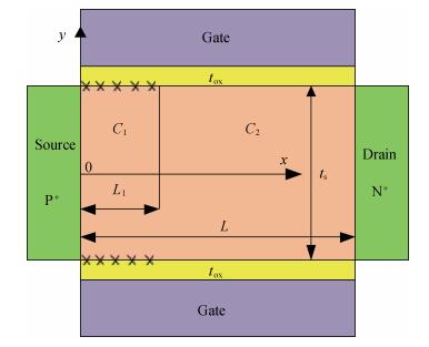
Processing math: 100%
J. Semicond. > 2017, Volume 38 > Issue 2 > 024004

SEMICONDUCTOR DEVICES

Two-dimensional analytical model of double-gate tunnel FETs with interface trapped charges including effects of channel mobile charge carriers

Huifang Xu1, and Yuehua Dai2

+ Author Affiliations

 Corresponding author: Huifang Xu, Email:xu0342@163.com

DOI: 10.1088/1674-4926/38/2/024004

PDF

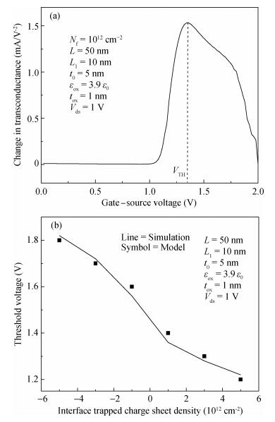
Abstract: A two-dimensional analytical model of double-gate (DG) tunneling field-effect transistors (TFETs) with interface trapped charges is proposed in this paper. The influence of the channel mobile charges on the potential profile is also taken into account in order to improve the accuracy of the models. On the basis of potential profile, the electric field is derived and the expression for the drain current is obtained by integrating the BTBT generation rate. The model can be used to study the impact of interface trapped charges on the surface potential, the shortest tunneling length, the drain current and the threshold voltage for varying interface trapped charge densities, length of damaged region as well as the structural parameters of the DG TFET and can also be utilized to design the charge trapped memory devices based on TFET. The biggest advantage of this model is that it is more accurate, and in its expression there are no fitting parameters with small calculating amount. Very good agreements for both the potential, drain current and threshold voltage are observed between the model calculations and the simulated results.

Key words: double-gate tunnel field effect transistor (TFET)interface trapped chargesanalytical model

It is well known that the industry based on silicon faces many challenges due to the continuous scaling down the feature size[1-3]. Therefore, breakthroughs in materials science play a significant role in the future development of technology and various applications. In 2004, graphene was the first discovered two-dimensional (2D) material extracted as a single layer of carbon atoms that are bonded together in a hexagonal honeycomb lattice from graphite[4]. It had attracted worldwide attention owing to its unique properties, including ultra-high mobility[5] and thermal conductivity[6], transparency[7], and high Young's modulus[8]. By virtue of their outstanding contribution to graphene development, the graphene discoverers, Konstantin Novoselov and Andre Geim, were awarded the Nobel Prize for physics in 2010. Devices based on graphene have shown various promising applications such as transistors[9-11], supercapacitors[12], batteries[13], solar cells[14], speakers[15, 16], and thermal rectifiers[17], etc. In brief, graphene has blazed a new trail for developing 2D material and has a promising future from research laboratories to industrial applications. However, the on/off ratio of graphene transistors was limited to ~10 because of graphene’s vanishing bandgap.

Since graphene discovery, many kinds of 2D materials have been discovered and developed, such as hexagonal boron nitride (hBN)[18], elemental analogs of graphene[19], transition metal dichalcogenides (TMDCs), etc. Molybdenum disulfide (MoS2), one kind of transition metal dichalcogenide, has a bandgap. The bandgap of single-layer MoS2 and the few layers MoS2 are ~1.8 and ~1.2 eV, respectively[20]. The on/off ratio field-effect transistors based on MoS2 can reach ~108, which is far beyond graphene devices’ performance[21]. However, the relatively low charge carrier mobility at room temperature was a limitation for the applications of MoS2 material.

Black phosphorus (BP) has a puckered structure that is one of the few-layered crystals and demonstrates strong in-plane anisotropy. The phosphorus was first recorded in “The Book of Odes and Hymns” (诗经) that can be traced back to about three centuries ago in ancient China[22]. However, the Nobel Prize in Physics was awarded to Percy Williams Bridgman who first synthesized BP until the twentieth century[23]. With the development of exfoliation and thin-layer processing techniques, phosphorene (a single-layer BP) was exfoliated for the first time from bulk BP via the Scotch-tape method. BP is considered as a new member joining the two-dimensional material family[24-26]. BP is a semiconductor with thickness-dependent direct bandgap and the bandgap of BP can be tuned continuously from ~0.3 eV (bulk) to ~2 eV (monolayer)[27], which is located between graphene and MoS2. It means that BP is a natural wide spectrum detection material and especially has a promising potential to have a breakthrough in mid-infrared applications[28]. Besides, there are two distinct advantages for transistors based on BP because they balance the on/off ratio compared to graphene and MoS2[24, 29-32]. Furthermore, BP also has good thermal[33-36] and mechanical characteristics[37]. In a word, BP, a new member in the family of 2D materials, has increasingly attracted substantial research interests and offers an opportunity to complement conventional silicon-based devices in various applications.

In this review, as shown in Fig. 1, we will introduce the BP sandwich structure with hBN, BP homojunction devices, BP heterojunction devices with other 2D and 3D bulk materials, and BP doped by As with tunable bandgap. There are three important issues (interface contact, interfacial modification and carrier separation) related to the BP electrical and optoelectronic devices. (1) For BP interface contact, different work-function metals can enable different transport behaviors. If Au or Ni is used, since the work function of Au is close to the middle of the bandgap of BP, so BP FET shows bipolar transport[29]. If high work function metal Pd is used, BP FET shows more like a p-FET[53]. If low work function metal Al is used for BP, n-FET is formed[102]. Typically, there is a Fermi-pining effect between BP and contact, which needs further exploration for contact optimization. (2) BP suffers from stability issues[103]. There is POx forming on both sides of BP[104]. There are several ways to enhance the stability: hBN protection[61], AlOx protection[105], and chemical protection[106]. These methods are very efficient to enhance the stability of the BP film with long time. (3) For BP photodetectors, the carrier separation is the key to enable the photodetection. If the BP is intrinsic, the carrier separation can be speedy, but the photoresponsivity can be relatively low[81]. For intrinsic BP with a perfect lattice structure, the electron–hole pair can be separated easily in BP based on the photovoltaic effect. Youngblood et al. found the largest photocurrent produced under VG = –8 V with a high response bandwidth exceeding 3 GHz, which is related to the intrinsic region of BP under photovoltaic effect[81]. The photo-gating effect cannot dominate in the above case because the trapping center is not enough in high-quality BP. Supposing the BP is doped by E-field or chemical and there is carrier trapping during the separation (i.e. photo-gating effect), in that case, the photoresponsivity can be very high, but the speed can be relatively low. For doped BP with enough trapping centers due to the degradation in air, the photo-gating effect can dominate the photo-sensing behaviors. Guo et al. reported high gain BP photodetectors based on the largest photocurrent produced at the BP doped region, which is related to the doped region of BP under the photo-gating effect[70]. There is a trade-off between choosing high photoresponsivity and response-speed.

Figure  1.  (Color online) Overview of BP crystal structure and BP devices.

Hexagonal boron nitride is a large-bandgap and chemically stable two-dimensional dielectric material, usually forming a sandwich structure with black phosphorus (Fig. 2(a)). As shown in Fig. 2(b), density functional theory calculation shows that characters such as direct bandgap and linear dichroism are preserved when capping an hBN layer on to protect BP[39]. Cai et al. concludes that hBN is a suitable material for capping BP, protecting it against structural and chemical degradation while still maintaining its major electronic characteristics. The hBN layers’ surface is smoother than SiO2 and is free of dangling bonds and surface charge traps. Thus, hBN is widely used as a substrate to improve the transport properties of other 2D materials[40-44].

Figure  2.  (Color online) Black phosphorus sandwich structure integration with hBN and its band structure. (a) A 3D schematic of hBN/BP/hBN heterostructure. (b) The HSE06 calculation results of the band structure and the local density of states (LDOS) for the hBN/BP heterostructure. Modified with permission from Ref. [38] Copyright 2016 American Chemical Society, (b) Ref. [39] Copyright 2015 American Chemical Society.

Combining the advantages of hBN, researchers have realized the hBN/BP/hBN structure to improve the transport properties and stability of BP (Fig. 3(a)). Tao et al. calculated the physical properties of hBN/BP/hBN heterostructures with different hBN thicknesses[49]. Compared with monolayer (ML) BP, the bandgap of the hBN(1ML)/BP(ML)/hBN(1ML) trilayer structure was increased by 0.15 eV. However, when the thickness of hBN continuously increased, the bandgap of BP had little change. They also observed an increased hole and electron effective masses via increasing hBN thickness. Doganov et al. compared mobilities of different substrate dielectrics of BP-based FET as a function of temperature, including BP/SiO2, BP/hBN, and hBN/BP/hBN. These results show that the hBN substrate improves mobility compared with SiO2 due to the higher dielectric constant. Furthermore, the full encapsulation with hBN increased the mobility over 100 cm2/(V·s) as shown in Fig. 3(b)[45]. Geim et al. assembled hBN/BP/hBN heterostructure using the dry transfer method in an inert atmosphere. They used monolayer or bilayer hBN on top of BP to protect it from all gases and liquids, and the top hBN layer can let electrons tunnel through, so the electrical contacts can be evaporated onto it without etching openings in the encapsulation. They achieved field-effect mobility of over 4000 cm2/(V·s) for bulklike devices (>10 layers) and about 1200 cm2/(V·s) in a trilayer device (Fig. 3(c)). Moreover, it also showed long-term stability according to the experimental electrical results stored in the air. Quantum oscillations were observed in hBN/BP/hBN sandwiched structures[46]. Nathaniel et al. fabricated the structure with one-dimensional edge contact to metal electrodes. As temperature decreased, the transistor behaved as a gate-dependent metal–insulator transition and device mobility increased. At T = 1.5 K, the mobility reached as high as 4000 cm2/(V·s). Under the condition of moderate magnetic fields and low temperature, they observed gate-tunable Shubnikov de Haas (SdH) magneto-oscillations and Zeeman splitting with an estimated g-factor ~2[32]. Xiaolong et al. used a high-temperature annealing process to reduce the charge trap density in BP. They realized high field-effect mobility of 1350 cm2/(V·s) at room temperature and higher mobility of 2700 cm2/(V·s) at T = 1.7 K. Meanwhile, they observed quantum oscillations and zero Berry phase at the suitable magnetic field and low temperature[30].

Figure  3.  (Color online) Fabrication process and mobility of hBN/BP/hBN heterostructure devices. (a) A 3D schematic of hBN/BP/hBN heterostructure device fabrication process. (b) Mobility results of the different structures including BP/SiO2 (red), BP/hBN (green), and hBN/BP/hBN (blue). (c) Mobility results of the trilayer and 20-layer were measured at liquid helium temperatures. (d) Mobility as a function of temperature for different carrier densities were measured. (e) Quantum Hall states with filling factors from 2 to 12 are observed. (f) FET and Hall mobilities at different temperature. Modified with permission from (a) Ref. [30] Copyright Nature publishing group, (b) Ref. [45] Copyright AIP Publishing, (c) Ref. [46] Copyright 2015 American Chemical Society, (d) and (e) Ref. [47] Copyright 2016 American Chemical Society, (f) Ref. [48] Copyright 2018 American Chemical Society.

Quantum Hall (QH) effect was observed in hBN/BP/hBN two-dimensional electron systems (2DES). Likai et al. improved mobility of the system by placing the hBN-encapsulated BP on a graphite back gate. The graphite gate results in a high carrier Hall mobility up to 6000 cm2/(V·s) at temperatures T < 30 K. The high mobility enabled them to observe the integer QH effect in BP. QH plateaus were observed at integer filling factors ν from 1 to 7[50]. Long et al. measured hole mobility of the hBN/BP/hBN field-effect transistor on SiO2/Si substrate. The mobility was 5200 cm2/(V·s) at room temperature, and increased to 45 000 cm2/(V·s) at cryogenic temperatures (Fig. 3(d)). They observed QH plateaus at ν from 2 to 12 (Fig. 3(e))[47]. Chen et al. reported a systematic study for thin-layer BP-based hBN/BP/hBN structure. They achieved the high intrinsic saturation velocity of holes and electrons at room temperature. As shown in Fig. 3(f), the FET and Hall mobilities can reach up to 3388 and 2024 cm2/(V·s), respectively[48]. In order to compare the transport properties of black phosphorus BP and BP heterostructures, we list mobilities and on/off ratio for various BP and BP-related heterostructures at different experimental temperatures in Table 1. Most of the BP devices show mobility less than 1000 cm2/(V·s), while the hBN/BP/hBN sandwich structures show the improved mobility larger than 1000 cm2/(V·s). There is strong evidence that the hBN/BP/hBN can enhance the mobility.

Table  1.  Comparison of performance of FETs based on BP and BP heterostructures, including BP film thickness, structure, mobility, on/off ratio.
Film thickness (nm)StructureMobility (cm2/(V·s))On/off ratioExperimental temperature (K)Ref.
10BP286104Room temperature[24]
10BP984105Room temperature[29]
1.9BP1722.7×104Room temperature[51]
5BP205105Room temperature[52]
15BP1000104120 K
18.7BP170.5102Room temperature[53]
8.5BP4002×103Room temperature[54]
15BP310103~104Room temperature[55]
5BP180104~105Room temperature
5BP155104Room temperature[56]
8hBN/BP/hBN1350105Room temperature[30]
2700/1.7 K
/hBN/BP/hBN5200/Room temperature[47]
/45000/2 K
11hBN/BP/hBN1432103Room temperature[48]
3388/77 K
10BP17102Room temperature[57]
5BP1495103260 K[58]
6.5BP(K-doped)262104Room temperature[59]
2.5BP(Al-doped)1055.6×103Room temperature[60]
4.5hBN/graphene/BP63100Room temperature[61]
30BP/MoS2/104Room temperature[62]
72BP/MoS2/105Room temperature[63]
10–15Graphene/BP/80030 K[64]
DownLoad: CSV  | Show Table

The p–n junction is a fundamental building block for the realization of incumbent electronic and optoelectronic devices. In conventional semiconductors, substitutional doping is commonly used to gain n- or p-type characteristics. BP, an ambipolar 2D material, can form n–n, n–p, p–n, and p–p junctions by doping or combining with other 2D materials such as hBN or graphene, respectively. Buscema et al. fabricated p–n junctions based on 2D materials, namely, hBN and BP, which are gate dielectric and channel material, respectively. They observed photovoltaic properties and the detection wavelength up to the near-infrared. Meanwhile, the transfer curves can be turned into four operational quadrants by different gate voltages (Fig. 4)[65]. Liu et al. reported a controllable doping technique using Al atoms to realize a high-performance photovoltaic device, which enhanced 2.5 times electron mobility. The open-circuit voltage responsivity and a short-circuit current responsivity reached ~15.7 × 10³ V/W and ~6.2 mA/W at room temperature in the near-infrared (1550 nm), respectively[60]. Han et al. demonstrated that the electron mobility of BP could be increased one order of magnitude through in situ functionalization of potassium[59]. Recently, Tian et al. reported 2D junctions made of BP and graphene whose type of device can be controlled by the back gate and graphene gate[66]. BP is regarded as a promising material for high speed, high response, and comprehensive spectrum detection from visible to mid-IR at room temperature.

Figure  4.  (Color online) Drain current mapping and band diagrams of the few-layer black phosphorus PN junction. Drain current mapping at (a) + 100 mV and (b) –100 mV as a function of Vrg and VIg, respectively. (c) Schematic energy band diagrams of the different device configurations. Modified with permission from Ref. [65] Copyright 2014 Springer Nature.

In the conventional p–n homojunction, the p- and n-type regions are formed by chemically doping a bulk semiconductor depleted of free charge carriers, creating built-in potentials. However, 2D semiconductors like BP, graphene, and transition metal dichalcogenides (TMDCs) can stack, forming their unique van der Waals (vdW) structures, which are predicted to exhibit utterly different charge transport characteristics than bulk heterojunctions. The novel bulk crystals are composed of individual layers, in which the van der Waals forces vertically stack each layer instead of covalent bonds. Because of their particular structures, they have great potential for the next-generation electronic and optoelectronic applications[77-79]. BP could stack with other 2D materials to form heterojunctions that reveal unusual properties and new phenomena.

Two-dimensional materials such as graphene have exhibited excellent optical characteristics and offer an attractive prospect for next-generation optoelectronics applications. Graphene has been used for the wideband photodetection from ultraviolet to terahertz[80]. However, graphene photodetectors' dark current is very high due to the graphene lack of a bandgap. Youngblood et al. fabricated a gated multilayer black phosphorus photodetector. The device's dark current is only 220 nA (VG = −8 V, Vbias = −0.4 V). Moreover, the intrinsic responsivity can reach up to 135 and 657 mA/W in 11.5-nm- and 100-nm-thick devices at room temperature, respectively. In almost all aspects of their performance, BP photodetectors are superior to graphene photodetectors[81]. Hu et al. fabricated a 2D hybrid phosphorene and graphene nanocomposite (Fig. 5(a)) and calculated the electronic bandgap using HSE06 method (Fig. 5(b)). The results show that the Fermi velocity of graphene at the Dirac point is kept and open a small bandgap (58 meV), which shows field-effect transistors' potential graphene/BP heterojunction[82]. Avsar et al. realized vertical field-effect transistors (VFETs) based on graphene/BP van der Waals heterostructure, which achieved an on/off ratio of ~100 at room temperature (Fig. 5(c))[61]. Kang et al. realized an on/off ratio of over 800 at 30 K and high on-state current densities of over 1600 A/cm2 in graphene/BP VFETs (Fig. 5(d))[64]. Besides, BP/graphene composite has a widely attracted ion battery research field due to the highest theoretical capacity of phosphorus, high electronic conductivity, mechanical strength, and fast reaction kinetics of graphene[83-86].

Figure  5.  (Color online) Bandgap and structure of graphene/BP heterojunction. (a) The top and side views of schematics of BP (violet)/graphene (gray) heterojunction. (b) The HSE06 calculation results of the band structure are graphene, phosphorene and graphene/BP heterojunction, respectively. (c) Transfer characteristic curves for an encapsulated device by measuring under both vacuum and ambient conditions. The inset shows a nonencapsulated device test. (d) Transfer characteristic curves at ranging various temperatures from 300 to 30 K in 30 K steps. Modified with permission from (a) and (b) Ref. [82] Copyright Royal Society of Chemistry, (c) Ref. [61] Copyright 2015 American Chemical Society, (d) Ref. [64] Copyright 2016 American Chemical Society.

TMDCs are atomically thin two-dimensional semiconductors of the type MX2. M is a transition metal atom (Mo, Re, etc.) and X is a chalcogen atom (S, Se, etc.). Molybdenum disulfide (MoS2) is the most exciting material in the TMDCs owing to its robustness[87]. MoS2 has been reported in the research of photodetectors due to unique optoelectronic properties[88-90]. BP-based optoelectronic devices are also widely researched, especially in the advantages of the near-infrared and infrared bands due to the lattice structure and band structure of BP[67-71]. Deng et al. designed a gate-tunable p–n diode based on a p-type BP/n-type monolayer MoS2 van der Waals p–n heterojunction which is the first 2D heterostructure demonstrated using black phosphorus. In the experiments, monolayer MoS2 was synthesized by chemical vapor deposition (CVD) on 285 nm SiO2/p+-doped Si substrate, and the BP was mechanically exfoliated on the monolayer MoS2. The thicknesses of the few-layer BP flake and monolayer MoS2 are 11 and 0.9 nm, respectively. The diodes based on 2D materials achieved a maximum photodetection responsivity of 418 mA/W and photovoltaic energy generation with an external quantum efficiency of 0.3% under the illumination of 633 nm He–Ne laser[72]. Taking advantage of BP bandgap in the infrared, Ye et al. fabricated a diode based on BP/MoS2 heterojunction as shown in Fig. 6(a). It realized microsecond response speed ~15 μs, which is 2 to 3 orders higher than that of the BP-based non-heterojunction photodetector in the near-infrared (Fig. 6(b))[74]. Kwak et al. performed a BP/WS2 heterojunction device at 405 nm and solar spectrum. The external quantum efficiency and the photovoltaic efficiencies are 4.4% and 4.6%, respectively, which shows potential for photovoltaic applications[91]. In addition to combining two materials, the structure's heterojunction has also been reported. Li et al. realized a bipolar phototransistor based on WSe2/BP/MoS2 heterostructure (Fig. 6(c)). As shown in Fig. 6(d), a broadband detector has a high responsivity of 6.32 A/W at visible light and 1.12 A/W at the infrared light, respectively[75]. The value of the photoresponsivity is an order of magnitude higher than that of the detector based on the WSe2/BP heterostructure. Besides, Srivastava et al. fabricated a BP/rhenium disulfide (ReS2) broken-gap van der Waals heterojunction device as shown in Fig. 6(e). Its photoresponsivity and the maximum external quantum efficiency (EQE) can reach up to 8 mA/W (Fig. 6(f)) and 0.3% under illustration under the illumination of 532 nm laser[76].

Figure  6.  (Color online) The photodetectors based on TMDCs/BP heterojunctions. (a) A 3D schematic of the BP/MoS2 heterojunction device. (b) On/off switching characteristics of the BP/MoS2 junction device under illumination of 1.55 μm laser (Laser power 96.2 μW) at different bias voltages. The rise time and the decay were 15 μs and 70 μs, respectively. (c) A 3D schematic of the WSe2/BP/MoS2 heterojunction device. (d) Photoresponsivity and photogain of the WSe2/BP/MoS2 heterojunction device as a function of wavelength, respectively. (e) A 3D schematic diagram of the ReS2/BP heterojunction device. (f) Current rectifying output characteristics as a function of incident laser power values under illumination of 532 nm laser. Modified with permission from (a) and (b) Ref. [74] Copyright 2016 American Chemical Society, (c) and (d) Ref. [75] Copyright 2017 American Chemical Society, (e) and (f) Ref. [76] Copyright 2019 American Chemical Society.

Depending on the carrier transport path, the FET structure based on vdW heterostructures is mainly divided into two categories: lateral heterojunction structure and vertical heterojunction structure. In a lateral heterojunction, the "edge-to-edge" structure allows carriers to conduct primaries in the material plane. However, the "up–down" structure allows carriers to conduct primarily between layers of material for a vertical heterojunction. Xu et al. fabricated a tunneling field-effect transistor based on a BP/MoS2 junction. The device's subthreshold swing (SS) values were ~65 and 51 mV/dec at room temperature and 160 K, respectively[62]. For vertical heterojunctions, they are mainly used for vertical field-effect transistors. This type of device's implementation is mainly due to the excellent quality interlayer conductivity of the two-dimensional semiconductor material. Liu et al. realized a BP/MoS2 tunneling heterojunction diode (Fig. 7(a)). They observed three kinds of diode characteristics, including a backward rectifying diode, a Zener diode, and a forward rectifying diode tuned by the thickness of BP (Fig. 7(b))[63]. Miao et al. realized a truly vertical p–n heterojunction diode based on MoS2/BP heterojunction (Fig. 7(c)). The p–n junction of the vertical structure exhibits a higher on current density than that of the lateral p–n junction. Moreover, they used MoS2 to isolate the effects of air increasing device lifetime (Fig. 7(d))[92]. A comparison of photodetectors based on BP and BP heterostructures is listed in Table 2. The BP/MoS2 heterojunction device shows a faster photo-response speed down to 15 μs than BP FETs around 1 ms.

Figure  7.  (Color online) Structure and performance of the lateral and vertical BP/MoS2 heterostructures. (a) A 3D schematic of the BP/MoS2 heterojunction device. (b) The diode current (Id) as a function of the voltage across the diode at different thicknesses of BP which are 9, 36 and 61 nm, respectively. (c) A schematic diagram of the BP/MoS2 heterostructure device cross-section. (d) I–V characteristics of vertical and lateral BP/MoS2 heterojunction diodes. The inset shows semilogarithmic scale plot of the same I–V curves. Modified with permission from (a) and (b) Ref. [63] Copyright 2017 American Chemical Society, (c) and (d) Ref. [92] Copyright 2017 American Chemical Society.
Table  2.  Comparison of performance of photodetectors based on BP and BP-related heterostructures, including film thickness, structure, spectral range, responsivity, specific detectivity and response time.
Film thickness (nm)StructureSpectral rangeResponsivity (A/W)Specific detectivity (Jones)Response time (ms)Ref.
BP: 3–8BPVisible to near-infrared4.8 × 10–3 (640 nm)>103~1 [67]
BP: ~4.5BPNear-ultraviolet to near-infrared9 × 104 (405 nm)3 × 10¹³~1 [68]
BP: 8BPVisible to near-infrared4.3 × 106 (633 nm, 300 K)
7 × 10⁶ (633 nm, 20 K)
/5 [69]
BP: ~12BP532 nm82//[70]
BP: 28, 47, 302BP830 nm2.421.833 × 1082.5 [71]
BP: ~22BP/MoS2633 nm0.418//[72]
BP: ~10, MoS2: ~4.8BP/MoS2532 nm~0.17//[73]
BP: ~22, MoS2: ~12BP/MoS2Visible to near-infrared22.3 (532 nm)
153.4 (1.55 μm)
3.1 × 10¹¹ (532 nm)
2.13 × 10⁹ (1.55 μm)
0.015
/
[74]
BP: 5, ReS2: 12BP/ReS2532 nm8//[75]
WSe2: ~43, BP: ~40, MoS2: ~34WSe2/BP/MoS2Visible to near-infrared6.32 (532 nm)
1.12 (1.55 μm)
1.25 × 10¹¹ (532 nm)
2.21 × 10¹⁰ (1.55 μm)
/[76]
DownLoad: CSV  | Show Table

The 2D material can be combined with 3D bulk material to form a new heterojunction due to their atomic thin body thickness and the lack of dangling bonds on the surfaces. The integration of 2D material with bulk material can also promote industry applications. The mixed-dimensional 2D/3D vdW heterostructures can improve optical absorption cross-sections than all-2D vdW heterostructures[93]. Gehring et al. transferred a thin-layer BP (~15 nm) sheet onto Te-doped GaAs substrate to form a heterojunction. The maximum EQE of the device can reach 9.7% under the illumination of 514 nm laser at zero bias (Fig. 8(a)) and be increased to 31% at a bias of –2.5 V[94]. Besides, 2D–3D p–n heterojunctions can become easily doped and have a high breakdown electric field for field-effect devices. Li et al. reported a vdW heterojunction JFET based on p-type BP and n-type β-Ga2O3. It exhibits excellent rectification characteristics and low reverse current in the order of picoamperes. Moreover, the source–drain current switching ratio can reach 107 (Fig. 8(b))[96]. Bi et al. realized two kinds of structures: tunnel field-effect transistor (TFET) and junction field-effect transistor (JFET) via the integration of InGaZnO and BP. The TFET’s current switching ratio achieved over 105, and the device's SS values was about 11 mV/dec. Meanwhile in BP/InGaZnO heterostructure JFET, it also shows on/off ratio over 105, almost no hysteresis and larger SS of 83 mV/dec due to the limitation of thermal emission (Fig. 8(c))[109].

Figure  8.  (Color online) Performance of BP/ 3D bulk material heterojunction device. (a) EQE as a function of laser power for different laser light wavelengths at zero source–drain bias based on BP/GaAs heterojunction. (b) Semi-log plot of the transfer characteristics of the JFET based on BP/β-Ga2O3 heterojunction. (c) The transfer characteristics of BP/InGaZnO JFET. The inset shows the corresponding µFE value. Modified with permission from (a) Ref. [94] Copyright AIP publishing, (b) Ref. [96] Copyright 2020 IOP, (c) Ref. [109] Copyright 2020 John Wiley and Sons.

Black phosphorus doped by arsenic or black arsenic–phosphorus (b-AsP), a family of layered semiconductors, has attracted extensive attention due to the excellent tunability of bandgaps. Liu et al. demonstrated the bandgap could be tuned to 0.15 eV smaller than BP (0.3 eV). It means that the detection range of the photodetectors based on b-AsP can reach the long-wavelength infrared (LWIR) (Figs. 9(a) and 9(b))[95]. Long et al. fabricated long-wavelength IR, the detection range up to 8.2 μm, photodetectors based on b-AsP. They achieved fast photoresponse (0.54 ms) tested in the mid-wavelength infrared, as shown in Fig. 9(c). Furthermore, this type of device had low dark noise at room temperature whose peak specific detectivity value can reach up to 9.2 × 10⁹ Jones (Fig. 9(d))[97]. B-AsP can also be combined with hBN to form a sandwich structure the same as BP. Yuan et al. fabricated a photodetector based on hBN/b-As0.83P0.17/hBN structure, which achieved good responsivity in the mid-infrared. Moreover, the air stability of the type of device enhanced owing to the hBN encapsulation[98].

Figure  9.  (Color online) Performance of the related b-AsP photodetectors. (a) Infrared absorption as a function of wavenumber for different samples including b-P, b-As0.25P0.75, b-As0.4P0.6 and b-As0.83P0.17, respectively. (b) Bandgap and wavelength as a function of different composition-tunable b-AsxP1−x or different polarization angle of the same composition, respectively. (c) Response curve as a function of time under illumination of 4.034 μm of the b-AsP photodetector. (d) Specific detectivity of different detectors as a function of wavelength including a thermistor bolometer, a PbSe detector, a b-AsP FET device and a b-AsP/MoS2 heterostructure. Modified with permission from (a) and (b) Ref. [95] Copyright John Wiley and Sons, (c) and (d) Ref. [97] Copyright AAAS.

In this review, heterostructures based on BP and their electrical and optical applications were discussed in detail. With the tremendous development of applications based on BP owing to its superior characteristics, an increasing number of novel devices based on BP broadly potential from laboratory research to practical use. To achieve this goal, researchers have to suffer from several challenging problems in further research and some possible solutions for dealing with the challenges as follows. (1) Synthesize high-quality wafer-scale crystalline and controllable thicknesses of BP. Fabrication of controllable thicknesses of BP with high quality is essential to design the BP-based devices and applications due to the thickness-dependent intrinsic direct bandgap. Most recently, Xu et al. show the large-area of BP grown on insulating silicon substrates by a gas-phase growth method[107]. It is promising to use the gas-phase growth method for wafer-scale BP. Until now, wafer-scale BP films have not been produced, which greatly hinder the BP-based large-scale applications. (2) Enhancement of long-term stability for BP-based device. Although many strategies have been attempted to improve BP devices' long-term stability, including functionalization, doping, and passivation, the experimental results still show a long distance with commercial grade products. To enhance the long-term stability for BP-based devices for commercial-grade products, a vacuum package can be considered. (3) The BP-based integrated circuits. The complementary inverter is the fundamental building block for logic circuits. Some BP-based complementary inverters have been fabricated via the adatom doping technique[68, 99, 100] or BP hybrids[101]. The uniformity of BP devices is still required to enable large-scale integrated circuits. The MoS2 1-bit microprocessor has been done[108]. The BP-based integrated circuits should come true soon, right after obtaining the wafer-scale BP film. If the large-scale BP can be obtained, there is also a great potential to enable an array of BP photodetectors for middle-IR photo-detection at room temperature, which could be better than the commercial HgCdTe middle-IR photo-detectors. Moreover, the high mobility and reasonable on/off ratio of the BP FET can enable next-generation flexible electronics and circuits with high performance, which is better than the organic-based flexible electronics.

This work was supported in part by Fundamental Research Project of National Institute of Metrology China under Grant AKYZZ2116, in part by National Natural Science Foundation of China under Grant 62022047, Grant 61874065 and Grant 51861145202, in part by the National Key R&D Program under Grant 2016YFA0200400, in part by the Research Fund from Beijing Innovation Center for Future Chip and the Independent Research Program of Tsinghua University under Grant 20193080047, in part by Young Elite Scientists Sponsorship Program by CAST under Grant 2018QNRC001, and in part by Fok Ying-Tong Education Foundation under Grant 171051.


[1]
Bardon M G, Neves H P, Puers R, et al. Pseudo-two-dimensional model for double-gate tunnel FETs considering the junctions depletion regions. IEEE Trans Electron Devices, 2010, 57(4):827 doi: 10.1109/TED.2010.2040661
[2]
Shiromani B R, Bahniman G, Bhupesh B. Temperature effect on hetero structure junctionless tunnel FET. J Semicond, 2015, 36(3):034002 doi: 10.1088/1674-4926/36/3/034002
[3]
Pranav K A. High performance 20 nm GaSb/InAs junctionless tunnel field effect transistor for low power supply. J Semicond, 2015, 36(2):24003 doi: 10.1088/1674-4926/36/2/024003
[4]
Sivasankaran K, Mallick P S. Impact of parameter fluctuations on RF stability performance of DG tunnel FET. J Semicond, 2015, 36(8):84001 doi: 10.1088/1674-4926/36/8/084001
[5]
Navjeet B, Subir K S. An analytical model for tunnel barrier modulation in triple metal double gate TFET. IEEE Trans Electron Devices, 2015, 62(7):2136 doi: 10.1109/TED.2015.2434276
[6]
Verhulst A S, Sorée B, Leonelli D, et al. Modeling the singlegate, double-gate, and gate-all-around tunnel field-effect transistor. Appl Phys Lett, 2007, 91(5):053102 doi: 10.1063/1.2757593
[7]
Pandey P, Vishnoi R, Kumar M J. A full-range dual material gate tunnel field effect transistor drain current model considering both source and drain depletion region band-to-band tunneling. J Comput Electron, 2015, 14(1):280 doi: 10.1007/s10825-014-0649-x
[8]
Giovanni B B, Elena G, Antonio G, et al. Dual-metal-gate InAs tunnel FET with enhanced turn-on steepness and high on current. IEEE Trans Electron Devices, 2014, 61(3):776 doi: 10.1109/TED.2014.2298212
[9]
Hraziia, Andrei V, Amara A, et al. An analysis on the ambipolar current in Si double-gate tunnel FETs. Solid-State Electron, 2012, 70:67 doi: 10.1016/j.sse.2011.11.009
[10]
Qiu Y X, Wang R S, Huang Q Q, et al. A comparative study on the impacts of interface traps on tunneling FET and MOSFET. IEEE Trans Electron Devices, 2014, 61(5):1284 doi: 10.1109/TED.2014.2312330
[11]
Huang X Y, Jiao G F, Cao W, et al. Effect of interface traps and oxide charge on drain current degradation in tunneling fieldeffect transistors. IEEE Electron Device Lett, 2010, 31(8):779 doi: 10.1109/LED.2010.2050456
[12]
Cao W, Yao C J, Jiao G F, et al. Improvement in reliability of tunneling field-effect transistor with p-n-i-n structure. IEEE Trans Electron Devices, 2011, 58(7):2122 doi: 10.1109/TED.2011.2144987
[13]
Arun Samuel T S, Balamurugan N B. Analytical modeling and simulation of germanium single gate silicon on insulator TFET. J Semicond, 2014, 35(3):034002 doi: 10.1088/1674-4926/35/3/034002
[14]
Rajat V, Jagadesh K M. Compact analytical model of dual material gate tunneling field-effect transistor using interband tunneling and channel transport. IEEE Trans Electron Devices, 2014, 61(6):1936 doi: 10.1109/TED.2014.2315294
[15]
Rajat V, Jagadesh K M. 2-D analytical model for the threshold voltage of a tunneling FET with localized charges. IEEE Trans Electron Devices, 2014, 61(9):3054 doi: 10.1109/TED.2014.2332039
[16]
Xu H F, Dai Y H, Li N, et al. A 2-D semi-analytical model of double-gate tunnel field-effect transistor. J Semicond, 2015, 36(5):054002 doi: 10.1088/1674-4926/36/5/054002
[17]
Gholizadeh M, Hosseini S E. A 2-D analytical model for doublegate tunnel FETs. IEEE Trans Electron Devices, 2014, 61(5):1494 doi: 10.1109/TED.2014.2313037
[18]
Narang R, Sasidhar Reddy K V, Saxena M, et al. a dielectricmodulated tunnel-FET-based biosensor for label-free detection:analytical modeling study and sensitivity analysis. IEEE Trans Electron Devices, 2012, 59(10):2809 doi: 10.1109/TED.2012.2208115
[19]
ATLAS User's Manual. Silvaco Int., Santa Clara, CA, 2009
[20]
Kao K H, Anne S V, William G V. Direct and indirect band-toband tunneling in germanium-based TFETs. IEEE Trans Electron Devices, 2012, 59(2):292 doi: 10.1109/TED.2011.2175228
[21]
Hurkx G A M, Klaassen D B M, Knuvers M P G. A new recombination model for device simulation including tunneling. IEEE Trans Electron Devices, 1992, 39(2):331 doi: 10.1109/16.121690
[22]
Dash S Mishra G P. A 2D analytical cylindrical gate tunnel FET (CG-TFET) model:impact of shortest tunneling distance. Adv Nat Sci:Nanosci Nanotechnol, 2015, 6:035005 doi: 10.1088/2043-6262/6/3/035005
[23]
Dash S Mishra G P. A new analytical threshold voltage model of cylindrical gate tunnel FET (CG-TFET). Superlattices Microstruct, 2015, 86:211 doi: 10.1016/j.spmi.2015.07.049
[24]
Tura A, Zhang Z N, Liu P C, et al. Vertical silicon p-n-p-n tunnel nMOSFET with MBE-grown tunneling junction. IEEE Trans Electron Devices, 2011, 58(7):1907 doi: 10.1109/TED.2011.2148118
Fig. 1.  (Color online) Cross-sectional schematics of DG TFET including localized interface charges.

Fig. 2.  (Color online) Surface potential of DG TFET for different gate--source biases.

Fig. 3.  (Color online) Surface potential of DG TFET for different Nf .

Fig. 4.  Transverse electric field of DG TFET with Nf .

Fig. 5.  (Color online) Surface potential for DG TFET with different L1 .

Fig. 6.  (Color online) Shortest tunneling length of DG TFET with different Nf .

Fig. 7.  (Color online) Shortest tunneling length of DG TFET with (a) different εox , (b) different ts , (c) different tox .

Fig. 8.  (Color online) Drain current as a function of gate-source voltage for DG TFET with different Nf .

Fig. 9.  (a) Extraction of threshold voltage of DG TFET by peak transconductance change method, (b) threshold voltage of DG TFET with different Nf .

Fig. 10.  Threshold voltage of DG TFET with (a) different εox , (b) different ts , (c) different tox .

[1]
Bardon M G, Neves H P, Puers R, et al. Pseudo-two-dimensional model for double-gate tunnel FETs considering the junctions depletion regions. IEEE Trans Electron Devices, 2010, 57(4):827 doi: 10.1109/TED.2010.2040661
[2]
Shiromani B R, Bahniman G, Bhupesh B. Temperature effect on hetero structure junctionless tunnel FET. J Semicond, 2015, 36(3):034002 doi: 10.1088/1674-4926/36/3/034002
[3]
Pranav K A. High performance 20 nm GaSb/InAs junctionless tunnel field effect transistor for low power supply. J Semicond, 2015, 36(2):24003 doi: 10.1088/1674-4926/36/2/024003
[4]
Sivasankaran K, Mallick P S. Impact of parameter fluctuations on RF stability performance of DG tunnel FET. J Semicond, 2015, 36(8):84001 doi: 10.1088/1674-4926/36/8/084001
[5]
Navjeet B, Subir K S. An analytical model for tunnel barrier modulation in triple metal double gate TFET. IEEE Trans Electron Devices, 2015, 62(7):2136 doi: 10.1109/TED.2015.2434276
[6]
Verhulst A S, Sorée B, Leonelli D, et al. Modeling the singlegate, double-gate, and gate-all-around tunnel field-effect transistor. Appl Phys Lett, 2007, 91(5):053102 doi: 10.1063/1.2757593
[7]
Pandey P, Vishnoi R, Kumar M J. A full-range dual material gate tunnel field effect transistor drain current model considering both source and drain depletion region band-to-band tunneling. J Comput Electron, 2015, 14(1):280 doi: 10.1007/s10825-014-0649-x
[8]
Giovanni B B, Elena G, Antonio G, et al. Dual-metal-gate InAs tunnel FET with enhanced turn-on steepness and high on current. IEEE Trans Electron Devices, 2014, 61(3):776 doi: 10.1109/TED.2014.2298212
[9]
Hraziia, Andrei V, Amara A, et al. An analysis on the ambipolar current in Si double-gate tunnel FETs. Solid-State Electron, 2012, 70:67 doi: 10.1016/j.sse.2011.11.009
[10]
Qiu Y X, Wang R S, Huang Q Q, et al. A comparative study on the impacts of interface traps on tunneling FET and MOSFET. IEEE Trans Electron Devices, 2014, 61(5):1284 doi: 10.1109/TED.2014.2312330
[11]
Huang X Y, Jiao G F, Cao W, et al. Effect of interface traps and oxide charge on drain current degradation in tunneling fieldeffect transistors. IEEE Electron Device Lett, 2010, 31(8):779 doi: 10.1109/LED.2010.2050456
[12]
Cao W, Yao C J, Jiao G F, et al. Improvement in reliability of tunneling field-effect transistor with p-n-i-n structure. IEEE Trans Electron Devices, 2011, 58(7):2122 doi: 10.1109/TED.2011.2144987
[13]
Arun Samuel T S, Balamurugan N B. Analytical modeling and simulation of germanium single gate silicon on insulator TFET. J Semicond, 2014, 35(3):034002 doi: 10.1088/1674-4926/35/3/034002
[14]
Rajat V, Jagadesh K M. Compact analytical model of dual material gate tunneling field-effect transistor using interband tunneling and channel transport. IEEE Trans Electron Devices, 2014, 61(6):1936 doi: 10.1109/TED.2014.2315294
[15]
Rajat V, Jagadesh K M. 2-D analytical model for the threshold voltage of a tunneling FET with localized charges. IEEE Trans Electron Devices, 2014, 61(9):3054 doi: 10.1109/TED.2014.2332039
[16]
Xu H F, Dai Y H, Li N, et al. A 2-D semi-analytical model of double-gate tunnel field-effect transistor. J Semicond, 2015, 36(5):054002 doi: 10.1088/1674-4926/36/5/054002
[17]
Gholizadeh M, Hosseini S E. A 2-D analytical model for doublegate tunnel FETs. IEEE Trans Electron Devices, 2014, 61(5):1494 doi: 10.1109/TED.2014.2313037
[18]
Narang R, Sasidhar Reddy K V, Saxena M, et al. a dielectricmodulated tunnel-FET-based biosensor for label-free detection:analytical modeling study and sensitivity analysis. IEEE Trans Electron Devices, 2012, 59(10):2809 doi: 10.1109/TED.2012.2208115
[19]
ATLAS User's Manual. Silvaco Int., Santa Clara, CA, 2009
[20]
Kao K H, Anne S V, William G V. Direct and indirect band-toband tunneling in germanium-based TFETs. IEEE Trans Electron Devices, 2012, 59(2):292 doi: 10.1109/TED.2011.2175228
[21]
Hurkx G A M, Klaassen D B M, Knuvers M P G. A new recombination model for device simulation including tunneling. IEEE Trans Electron Devices, 1992, 39(2):331 doi: 10.1109/16.121690
[22]
Dash S Mishra G P. A 2D analytical cylindrical gate tunnel FET (CG-TFET) model:impact of shortest tunneling distance. Adv Nat Sci:Nanosci Nanotechnol, 2015, 6:035005 doi: 10.1088/2043-6262/6/3/035005
[23]
Dash S Mishra G P. A new analytical threshold voltage model of cylindrical gate tunnel FET (CG-TFET). Superlattices Microstruct, 2015, 86:211 doi: 10.1016/j.spmi.2015.07.049
[24]
Tura A, Zhang Z N, Liu P C, et al. Vertical silicon p-n-p-n tunnel nMOSFET with MBE-grown tunneling junction. IEEE Trans Electron Devices, 2011, 58(7):1907 doi: 10.1109/TED.2011.2148118
1

Analytical model for the effects of the variation of ferrolectric material parameters on the minimum subthreshold swing in negative capacitance capacitor

Raheela Rasool, Najeeb-ud-Din, G. M. Rather

Journal of Semiconductors, 2019, 40(12): 122401. doi: 10.1088/1674-4926/40/12/122401

2

A compact two-dimensional analytical model of the electrical characteristics of a triple-material double-gate tunneling FET structure

C. Usha, P. Vimala

Journal of Semiconductors, 2019, 40(12): 122901. doi: 10.1088/1674-4926/40/12/122901

3

Two dimensional analytical model for a negative capacitance double gate tunnel field effect transistor with ferroelectric gate dielectric

Huifang Xu

Journal of Semiconductors, 2018, 39(10): 104004. doi: 10.1088/1674-4926/39/10/104004

4

Performance analysis of SiGe double-gate N-MOSFET

A. Singh, D. Kapoor, R. Sharma

Journal of Semiconductors, 2017, 38(4): 044003. doi: 10.1088/1674-4926/38/4/044003

5

Modeling the drain current and its equation parameters for lightly doped symmetrical double-gate MOSFETs

Mini Bhartia, Arun Kumar Chatterjee

Journal of Semiconductors, 2015, 36(4): 044003. doi: 10.1088/1674-4926/36/4/044003

6

Effects of interface trap density on the electrical performance of amorphous InSnZnO thin-film transistor

Yongye Liang, Kyungsoo Jang, S. Velumani, Cam Phu Thi Nguyen, Junsin Yi, et al.

Journal of Semiconductors, 2015, 36(2): 024007. doi: 10.1088/1674-4926/36/2/024007

7

A 2-D semi-analytical model of double-gate tunnel field-effect transistor

Huifang Xu, Yuehua Dai, Ning Li, Jianbin Xu

Journal of Semiconductors, 2015, 36(5): 054002. doi: 10.1088/1674-4926/36/5/054002

8

An improved analytical model of 4H-SiC MESFET incorporating bulk and interface trapping effects

M. Hema Lata Rao, N. V. L. Narasimha Murty

Journal of Semiconductors, 2015, 36(1): 014004. doi: 10.1088/1674-4926/36/1/014004

9

Analytical model for subthreshold current and subthreshold swing of short-channel double-material-gate MOSFETs with strained-silicon channel on silicon-germanium substrates

Pramod Kumar Tiwari, Gopi Krishna Saramekala, Sarvesh Dubey, Anand Kumar Mukhopadhyay

Journal of Semiconductors, 2014, 35(10): 104002. doi: 10.1088/1674-4926/35/10/104002

10

Dynamic threshold voltage operation in Si and SiGe source junctionless tunnel field effect transistor

Shibir Basak, Pranav Kumar Asthana, Yogesh Goswami, Bahniman Ghosh

Journal of Semiconductors, 2014, 35(11): 114001. doi: 10.1088/1674-4926/35/11/114001

11

Analytical modeling and simulation of germanium single gate silicon on insulator TFET

T. S. Arun Samuel, N. B. Balamurugan

Journal of Semiconductors, 2014, 35(3): 034002. doi: 10.1088/1674-4926/35/3/034002

12

An analytical model of the electric field distributions of buried superjunction devices

Haimeng Huang, Xingbi Chen

Journal of Semiconductors, 2013, 34(6): 064006. doi: 10.1088/1674-4926/34/6/064006

13

On-current modeling of short-channel double-gate (DG) MOSFETs with a vertical Gaussian-like doping profile

Sarvesh Dubey, Kumar Tiwari, S. Jit

Journal of Semiconductors, 2013, 34(5): 054001. doi: 10.1088/1674-4926/34/5/054001

14

Simulation study on short channel double-gate junctionless field-effect transistors

Meile Wu, Xiaoshi Jin, Rongyan Chuai, Xi Liu, Jong-Ho Lee, et al.

Journal of Semiconductors, 2013, 34(3): 034004. doi: 10.1088/1674-4926/34/3/034004

15

Analytical modeling of drain current and RF performance for double-gate fully depleted nanoscale SOI MOSFETs

Rajiv Sharma, Sujata Pandey, Shail Bala Jain

Journal of Semiconductors, 2012, 33(2): 024001. doi: 10.1088/1674-4926/33/2/024001

16

A two-dimensional analytical-model-based comparative threshold performance analysis of SOI-SON MOSFETs

Sanjoy Deb, Saptarsi Ghosh, N Basanta Singh, A K De, Subir Kumar Sarkar, et al.

Journal of Semiconductors, 2011, 32(10): 104001. doi: 10.1088/1674-4926/32/10/104001

17

Dual Material Gate SOI MOSFET with a Single Halo

Li Zunchao, Jiang Yaolin, Wu Jianmin

Chinese Journal of Semiconductors , 2007, 28(3): 327-331.

18

An Analytical Model for the Surface Electrical Field Distribution and Optimization of Bulk-Silicon Double RESURF Devices

Li Qi, Li Zhaoji, Zhang Bo

Chinese Journal of Semiconductors , 2006, 27(7): 1177-1182.

19

An Analytical Threshold Voltage Model for Fully Depleted SOI MOSFETs

Li Ruizhen, Han Zhengsheng

Chinese Journal of Semiconductors , 2005, 26(12): 2303-2308.

20

Analytical Modeling of Threshold Voltage for Double-Gate MOSFET Fully Comprising Quantum Mechanical Effects

Zhang Dawei, Tian Lilin,and Yu Zhiping

Chinese Journal of Semiconductors , 2005, 26(3): 429-435.

1. Wu, R., Zhang, H., Ma, H. et al. Synthesis, Modulation, and Application of Two-Dimensional TMD Heterostructures. Chemical Reviews, 2024, 124(17): 10112-10191. doi:10.1021/acs.chemrev.4c00174
2. Zhou, Z., Lv, J., Tan, C. et al. Emerging Frontiers of 2D Transition Metal Dichalcogenides in Photovoltaics Solar Cell. Advanced Functional Materials, 2024, 34(29): 2316175. doi:10.1002/adfm.202316175
3. Jiang, G., Yang, L., Peng, Y. et al. Fabrication strategies, applications and prospects of MXene titanium nitride (Tin+1NnTx): A mini review. Journal of Materials Research and Technology, 2024. doi:10.1016/j.jmrt.2024.04.233
4. Zhang, X., Li, R., Yu, Y. et al. Dark Current Mechanisms and Suppression Strategies for Infrared Photodetectors Based on Two-Dimensional Materials. Laser and Photonics Reviews, 2024, 18(5): 2300936. doi:10.1002/lpor.202300936
5. Alpomishev, E.K., Adamian, G.G., Antonenko, N.V. Two-dimensional open quantum system in dissipative bosonic heat bath, external magnetic field, and two time-dependent electric fields. Physical Review E, 2024, 109(4): 044125. doi:10.1103/PhysRevE.109.044125
6. Zou, B., Wang, S., Wang, Q. et al. Transport properties and electronic phase transitions in two-dimensional tellurium at high pressure. Applied Physics Letters, 2024, 124(10): 102105. doi:10.1063/5.0190275
7. Turbedaroglu, O., Kubanaliev, T., Alemdar, S. et al. Reduced Graphene Oxide/Few-Layer Phosphorene Binary Heterojunctions as Metal-Free Photocatalysts for the Sustainable Photoredox C-H Arylation of Heteroarenes. ACS Sustainable Chemistry and Engineering, 2024, 12(9): 3659-3670. doi:10.1021/acssuschemeng.3c07117
8. Dutta, T., Yadav, N., Wu, Y. et al. Electronic properties of 2D materials and their junctions. Nano Materials Science, 2024, 6(1): 1-23. doi:10.1016/j.nanoms.2023.05.003
9. Zhu, X., Cai, Z., Wu, Q. et al. 2D Black Phosphorus Infrared Photodetectors. Laser and Photonics Reviews, 2024. doi:10.1002/lpor.202400703
10. Mubarak, S., Byun, H.-S., Dhamodharan, D. et al. Functionalized black phosphorous-based polymer nanocomposites. Advances in Functionalized Polymer Nanocomposites: From Synthesis to Applications, 2024. doi:10.1016/B978-0-443-18860-2.00016-5
11. Alpomishev, E.K., Adamian, G.G., Antonenko, N.V. Quantum Hall and Shubnikov-de Haas Effects in Graphene within Non-Markovian Langevin Approach. Symmetry, 2024, 16(1): 7. doi:10.3390/sym16010007
12. Long, H., Liu, H., Wang, X. et al. Machine Vision Based on an Ultra-Wide Bandgap 2D Semiconductor AsSbO3. Advanced Functional Materials, 2023, 33(49): 2306241. doi:10.1002/adfm.202306241
13. Abdi, M., Astinchap, B. Optical properties of methyl-substituted germanane monolayer in the presence of the external magnetic field, strain and spin-orbit coupling. Journal of Physics Condensed Matter, 2023, 35(46): 465702. doi:10.1088/1361-648X/acee40
14. Viscardi, L., Intonti, K., Kumar, A. et al. Black Phosphorus Nanosheets in Field Effect Transistors with Ni and NiCr Contacts. Physica Status Solidi (B) Basic Research, 2023, 260(9): 2200537. doi:10.1002/pssb.202200537
15. Mohsseni Ahangar, R., Farmanzadeh, D. Effects of hexagonal boron nitride encapsulation on the electronic properties of Cu, Li, and O-doped black phosphorus monolayer. Physica B: Condensed Matter, 2023. doi:10.1016/j.physb.2023.414880
16. Han, Q., Jiang, Y., Liu, X. et al. Visible to Mid-Infrared Photodetector Based on Black Phosphorous-MoS2 Van Der Waals Heterojunction. IEEE Photonics Journal, 2023, 15(2): 2200405. doi:10.1109/JPHOT.2023.3241285
17. Yang, Q., Jin, W., Zhang, Q. et al. Mixed-modality speech recognition and interaction using a wearable artificial throat. Nature Machine Intelligence, 2023, 5(2): 169-180. doi:10.1038/s42256-023-00616-6
18. Peyvand, M.A., Ravaei, B., Zare, M. Fermi velocity and effective mass of quasiparticles in bilayer phosphorene nanoribbons. Canadian Journal of Physics, 2023, 101(8): 404-414. doi:10.1139/cjp-2022-0037
19. Haoran, L., Yuan, G., Hao, L. et al. Ultraviolet Photodetector Based on Wide Bandgap Two-Dimensional Semiconductor TlGaS2 | [宽带隙二维半导体 TlGaS2紫外探测器]. Zhongguo Jiguang/Chinese Journal of Lasers, 2023, 50(1): 0113015. doi:10.3788/CJL221103
20. Liu, J., Li, B., Li, Q. Two-Dimensional Doped Materials. Magnetochemistry, 2022, 8(12): 172. doi:10.3390/magnetochemistry8120172
21. Abdullah Ripain, A.H., Zulkifli, N.A.A., Tan, C.L. et al. Contributions of symmetric metal contacts on liquid exfoliation 2D-MoS2 flakes based MSM photodetector by spray pyrolysis: a CVD-free technique. Optical and Quantum Electronics, 2022, 54(12): 847. doi:10.1007/s11082-022-04253-y
22. Shen, Y., Dong, Z., Sun, Y. et al. The Trend of 2D Transistors toward Integrated Circuits: Scaling Down and New Mechanisms. Advanced Materials, 2022, 34(48): 2201916. doi:10.1002/adma.202201916
23. Lei, W., Wang, Y., Wu, S. et al. 2D Nanomaterials from Group VA Single-element: Research Progress in Biomedical Fields | [VA 族单元素二维纳米材料在生物医用领域的研究进展]. Wuji Cailiao Xuebao/Journal of Inorganic Materials, 2022, 37(11): 1181-1191. doi:10.15541/jim20220089
24. Hou, S., Guo, Z., Xiong, T. et al. Optical and electronic anisotropy of a 2D semiconductor SiP. Nano Research, 2022, 15(9): 8579-8586. doi:10.1007/s12274-022-4481-5
25. Cheng, Z., Wang, C., Wu, X. et al. Review in situ transmission electron microscope with machine learning. Journal of Semiconductors, 2022, 43(8): 081001. doi:10.1088/1674-4926/43/8/081001
26. Alam, K.. Transport and performance study of double-walled black phosphorus nanotube transistors. Semiconductor Science and Technology, 2022, 37(8): 085003. doi:10.1088/1361-6641/ac773e
27. Cao, Y., Li, C., Deng, J. et al. Enhanced photodetector performance of black phosphorus by interfacing with chiral perovskite. Nano Research, 2022, 15(8): 7492-7497. doi:10.1007/s12274-022-4378-3
28. Malik, M., Iqbal, M.A., Choi, J.R. et al. 2D Materials for Efficient Photodetection: Overview, Mechanisms, Performance and UV-IR Range Applications. Frontiers in Chemistry, 2022. doi:10.3389/fchem.2022.905404
29. Wu, F., Tian, H., Shen, Y. et al. Vertical MoS2 transistors with sub-1-nm gate lengths. Nature, 2022, 603(7900): 259-264. doi:10.1038/s41586-021-04323-3
30. Deng, N., Wang, P., Zhang, E. et al. Low-frequency 1/f noise in a graphene/silicon X-ray detector. 2021. doi:10.1109/3M-NANO49087.2021.9599829
  • Search

    Advanced Search >>

    GET CITATION

    Ningqin Deng, He Tian, Jian Zhang, Jinming Jian, Fan Wu, Yang Shen, Yi Yang, Tian-Ling Ren. Black phosphorus junctions and their electrical and optoelectronic applications[J]. Journal of Semiconductors, 2021, 42(8): 081001. doi: 10.1088/1674-4926/42/8/081001
    N Q Deng, H Tian, J Zhang, J M Jian, F Wu, Y Shen, Y Yang, T L Ren, Black phosphorus junctions and their electrical and optoelectronic applications[J]. J. Semicond., 2021, 42(8): 081001. doi: 10.1088/1674-4926/42/8/081001.
    shu

    Export: BibTex EndNote

    Article Metrics

    Article views: 3701 Times PDF downloads: 52 Times Cited by: 30 Times

    History

    Received: 23 May 2016 Revised: 06 July 2016 Online: Published: 01 February 2017

    Catalog

      Email This Article

      User name:
      Email:*请输入正确邮箱
      Code:*验证码错误
      Ningqin Deng, He Tian, Jian Zhang, Jinming Jian, Fan Wu, Yang Shen, Yi Yang, Tian-Ling Ren. Black phosphorus junctions and their electrical and optoelectronic applications[J]. Journal of Semiconductors, 2021, 42(8): 081001. doi: 10.1088/1674-4926/42/8/081001 ****N Q Deng, H Tian, J Zhang, J M Jian, F Wu, Y Shen, Y Yang, T L Ren, Black phosphorus junctions and their electrical and optoelectronic applications[J]. J. Semicond., 2021, 42(8): 081001. doi: 10.1088/1674-4926/42/8/081001.
      Citation:
      Huifang Xu, Yuehua Dai. Two-dimensional analytical model of double-gate tunnel FETs with interface trapped charges including effects of channel mobile charge carriers[J]. Journal of Semiconductors, 2017, 38(2): 024004. doi: 10.1088/1674-4926/38/2/024004 ****
      H F Xu, Y H Dai. Two-dimensional analytical model of double-gate tunnel FETs with interface trapped charges including effects of channel mobile charge carriers[J]. J. Semicond., 2017, 38(2): 024004. doi: 10.1088/1674-4926/38/2/024004.

      Two-dimensional analytical model of double-gate tunnel FETs with interface trapped charges including effects of channel mobile charge carriers

      DOI: 10.1088/1674-4926/38/2/024004
      Funds:

      the University Natural Science Research Key Project of Anhui Province KJ2016A169

      the National Natural Science Foundation of China 61376106

      the Introduced Talents Project of Anhui Science and Technology University 

      Project supported by the National Natural Science Foundation of China (No. 61376106), the University Natural Science Research Key Project of Anhui Province (No. KJ2016A169), and the Introduced Talents Project of Anhui Science and Technology University

      More Information
      • Corresponding author: Huifang Xu, Email:xu0342@163.com
      • Received Date: 2016-05-23
      • Revised Date: 2016-07-06
      • Published Date: 2017-02-01

      Catalog

        /

        DownLoad:  Full-Size Img  PowerPoint
        Return
        Return