Fig. 1.
Structure of In0.46Ga0.54N/Si tandem solar cell with In0.5Ga0.5N (n+)/Si (p+) and GaAs (n+)/GaAs (p+) tunnel junctions.
SEMICONDUCTOR DEVICES
M. Benaicha1, 2, L. Dehimi1, 2 and Nouredine Sengouga1, 2,
Corresponding author: Sengouga Nouredine, Email: nourseng@gmail.com
Abstract: A comprehensive study of high efficiency In0.46Ga0.54N/Si tandem solar cell is presented. A tunnel junction (TJ) was needed to interconnect the top and bottom sub-cells. Two TJ designs, integrated within this tandem: GaAs (n+)/GaAs (p+) and In0.5Ga0.5N (n+)/Si (p+) were considered. Simulations of GaAs (n+)/GaAs (p+) and In0.5Ga0.5N (n+)/Si (p+) TJ I-V characteristics were studied for integration into the proposed tandem solar cell. A comparison of the simulated solar cell I-V characteristics under 1 sun AM1.5 spectrum was discussed in terms of short circuit current density (Jsc), open circuit voltage (VOC), fill factor (FF) and efficiency (η) for both tunnel junction designs. Using GaAs (n+)/GaAs (p+) tunnel junction, the obtained values of Jsc=21.74 mA/cm2, VOC=1.81 V, FF=0.87 and η=34.28%, whereas the solar cell with the In0.5Ga0.5N/Si tunnel junction reported values of Jsc=21.92 mA/cm2, VOC=1.81 V, FF=0.88 and η=35.01%. The results found that required thicknesses for GaAs (n+)/GaAs (p+) and In0.5Ga0.5N (n+)/Si (p+) tunnel junctions are around 20 nm, the total thickness of the top InGaN can be very small due to its high optical absorption coefficient and the use of a relatively thick bottom cell is necessary to increase the conversion efficiency.
Keywords: InGaN/Si, tandem solar cells, tunnel junctions, simulation
| [1] |
Feng S W, Lai C M, Tu L W. Numerical simulations of the current-matching effect and operation mechanisms on the performance of InGaN/Si tandem cells. Nanoscale Res Lett, 2014, 9: 652 doi: 10.1186/1556-276X-9-652
|
| [2] |
Jani O, Ferguson I, Honsberg C, et al. Design and characterization of GaN/InGaN solar cells. Appl Phys Lett, 2007, 91: 132117 https://www.researchgate.net/publication/235000528_Design_and_characterization_of_GaNInGaN_solar_cells
|
| [3] |
Nanishi Y, Saito Y, Yamaguchi T. RF-molecular beam epitaxy growth and properties of InN and related alloys. Jpn J Appl Phys, Part 1, 2003, 42: 2549 doi: 10.1143/JJAP.42.2549
|
| [4] |
Zheng Y D, Mihara A, Yamamoto A. Analysis of InxGa1-xN/Si p-n heterojunction solar cells and the effects of spontaneous and piezoelectric polarization charges. J App Phys, 2013, 103: 153509
|
| [5] |
Li Z D, Xiao H L, Wang X L, et al. Theoretical simulations of InGaN/Si mechanically stacked two-junction solar cell. Physica B, 2013, 414: 110 doi: 10.1016/j.physb.2013.01.026
|
| [6] |
Hsu L, Walukiewicz W. Modeling of InGaN/Si tandem solar cells. J Appl Phys, 2008, 104: 024507
|
| [7] |
Brown G F, Ager J W, Walukiewicz W, et al. Finite element simulations of compositionally graded InGaN solar cells. Sol Energy Mater Sol Cells, 2010, 94: 478 doi: 10.1016/j.solmat.2009.11.010
|
| [8] |
Michael S, Lavery J. 23rd European Photovoltaic Solar Energy Conference, 1-5 September 2008, Valencia, Spain
|
| [9] |
Zhao Y M, Dong J R, Li K L, et al. InGaAsP/InGaAs tandem photovoltaic devices for four-junction solar cells. J Semicond, 2015, 36(4): 044011
|
| [10] |
Wang H X, Zheng X H, Gan X Y, et al. Designing of 1 eV GaNAs/GaInAs superlattice subcell in current-matched four-junction solar cell. J Semicond, 2016, 37(1): 014004 http://www.cnki.com.cn/Article/CJFDTotal-BDTX201601010.htm
|
| [11] |
Cao K W, Liu T, Liu J M, et al. Evaluation of four inch diameter VGF-Ge substrates used for manufacturing multi-junction solar cell. J Semicond, 2016, 37(6): 063002 doi: 10.1088/1674-4926/37/6/063002
|
| [12] |
Wu J, Walukiewicz W. Band gaps of InN and group Ⅲ nitride alloys. Superlattice Microstruct, 2003, 34: 63 https://www.researchgate.net/publication/222355392_Band_gaps_of_InN_and_group_III_nitride_alloys
|
| [13] |
Zhang X B, Wang X L, Xiao H L, et al Simulation of In0.56Ga0.35N single-junction solar cell. J Phys D, 2007, 40: 7335 http://www.academia.edu/9178398/Design_of_Multijunction_Photovoltaic_Cells_Optimized_for_Varied_Atmospheric_Conditions
|
| [14] |
Levinshtein M E, Rumyantsev S L, Shur M S. Properties of advanced semiconductor materials: GaN, AlN, InN, BN, SiC, SiGe. New York: John Wiley & Sons, 2001
|
| [15] |
Inushima T, Higashiwaki M, Matsui T. Optical properties of Si-doped InN grown on sapphire (0001). Phys Rev B, 2003, 68: 1
|
| [16] |
Levinshtein M E, Rumyantsev S L, Shur M S. Properties of advanced semiconductor materials. Wiley Chichester, UK, 2001: 1 http://www.gbv.de/dms/ilmenau/toc/314774785.PDF
|
| [17] |
Mnatsakanov T T, Levinshtein M E, Pmortseva L I, et al. Carrier mobility model for GaN. Solid-State Electron, 2003, 47: 111 https://www.researchgate.net/publication/222028285_Carrier_mobility_model_for_GaN
|
| [18] |
Hsu L, Jones R E, Li S X, et al. Electron mobility in InN and Ⅲ-N alloys. J Appl Phys, 2007, 102: 073705
|
| [19] |
Adachi S. The handbook on optical constants of semiconductors in tables and figures. World Scientific, 2012
|
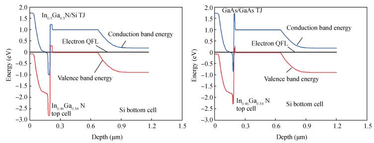
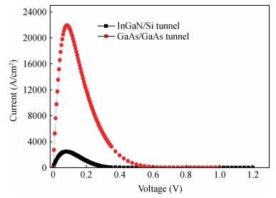
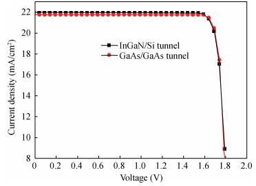
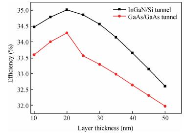
Table 1. Parameters used to calculate the carrier mobility of Eq. (8)[18].

|
| [1] |
Feng S W, Lai C M, Tu L W. Numerical simulations of the current-matching effect and operation mechanisms on the performance of InGaN/Si tandem cells. Nanoscale Res Lett, 2014, 9: 652 doi: 10.1186/1556-276X-9-652
|
| [2] |
Jani O, Ferguson I, Honsberg C, et al. Design and characterization of GaN/InGaN solar cells. Appl Phys Lett, 2007, 91: 132117 https://www.researchgate.net/publication/235000528_Design_and_characterization_of_GaNInGaN_solar_cells
|
| [3] |
Nanishi Y, Saito Y, Yamaguchi T. RF-molecular beam epitaxy growth and properties of InN and related alloys. Jpn J Appl Phys, Part 1, 2003, 42: 2549 doi: 10.1143/JJAP.42.2549
|
| [4] |
Zheng Y D, Mihara A, Yamamoto A. Analysis of InxGa1-xN/Si p-n heterojunction solar cells and the effects of spontaneous and piezoelectric polarization charges. J App Phys, 2013, 103: 153509
|
| [5] |
Li Z D, Xiao H L, Wang X L, et al. Theoretical simulations of InGaN/Si mechanically stacked two-junction solar cell. Physica B, 2013, 414: 110 doi: 10.1016/j.physb.2013.01.026
|
| [6] |
Hsu L, Walukiewicz W. Modeling of InGaN/Si tandem solar cells. J Appl Phys, 2008, 104: 024507
|
| [7] |
Brown G F, Ager J W, Walukiewicz W, et al. Finite element simulations of compositionally graded InGaN solar cells. Sol Energy Mater Sol Cells, 2010, 94: 478 doi: 10.1016/j.solmat.2009.11.010
|
| [8] |
Michael S, Lavery J. 23rd European Photovoltaic Solar Energy Conference, 1-5 September 2008, Valencia, Spain
|
| [9] |
Zhao Y M, Dong J R, Li K L, et al. InGaAsP/InGaAs tandem photovoltaic devices for four-junction solar cells. J Semicond, 2015, 36(4): 044011
|
| [10] |
Wang H X, Zheng X H, Gan X Y, et al. Designing of 1 eV GaNAs/GaInAs superlattice subcell in current-matched four-junction solar cell. J Semicond, 2016, 37(1): 014004 http://www.cnki.com.cn/Article/CJFDTotal-BDTX201601010.htm
|
| [11] |
Cao K W, Liu T, Liu J M, et al. Evaluation of four inch diameter VGF-Ge substrates used for manufacturing multi-junction solar cell. J Semicond, 2016, 37(6): 063002 doi: 10.1088/1674-4926/37/6/063002
|
| [12] |
Wu J, Walukiewicz W. Band gaps of InN and group Ⅲ nitride alloys. Superlattice Microstruct, 2003, 34: 63 https://www.researchgate.net/publication/222355392_Band_gaps_of_InN_and_group_III_nitride_alloys
|
| [13] |
Zhang X B, Wang X L, Xiao H L, et al Simulation of In0.56Ga0.35N single-junction solar cell. J Phys D, 2007, 40: 7335 http://www.academia.edu/9178398/Design_of_Multijunction_Photovoltaic_Cells_Optimized_for_Varied_Atmospheric_Conditions
|
| [14] |
Levinshtein M E, Rumyantsev S L, Shur M S. Properties of advanced semiconductor materials: GaN, AlN, InN, BN, SiC, SiGe. New York: John Wiley & Sons, 2001
|
| [15] |
Inushima T, Higashiwaki M, Matsui T. Optical properties of Si-doped InN grown on sapphire (0001). Phys Rev B, 2003, 68: 1
|
| [16] |
Levinshtein M E, Rumyantsev S L, Shur M S. Properties of advanced semiconductor materials. Wiley Chichester, UK, 2001: 1 http://www.gbv.de/dms/ilmenau/toc/314774785.PDF
|
| [17] |
Mnatsakanov T T, Levinshtein M E, Pmortseva L I, et al. Carrier mobility model for GaN. Solid-State Electron, 2003, 47: 111 https://www.researchgate.net/publication/222028285_Carrier_mobility_model_for_GaN
|
| [18] |
Hsu L, Jones R E, Li S X, et al. Electron mobility in InN and Ⅲ-N alloys. J Appl Phys, 2007, 102: 073705
|
| [19] |
Adachi S. The handbook on optical constants of semiconductors in tables and figures. World Scientific, 2012
|


Article views: 5805 Times PDF downloads: 67 Times Cited by: 0 Times
Received: 11 October 2016 Revised: 03 November 2016 Online: Published: 01 April 2017
| Citation: |
M. Benaicha, L. Dehimi, Nouredine Sengouga. Simulation of double junction In0.46Ga0.54N/Si tandem solar cell[J]. Journal of Semiconductors, 2017, 38(4): 044002. doi: 10.1088/1674-4926/38/4/044002
****
M Benaicha, L Dehimi, N Sengouga. Simulation of double junction In0.46Ga0.54N/Si tandem solar cell[J]. J. Semicond., 2017, 38(4): 044002. doi: 10.1088/1674-4926/38/4/044002.

|
| [1] |
Feng S W, Lai C M, Tu L W. Numerical simulations of the current-matching effect and operation mechanisms on the performance of InGaN/Si tandem cells. Nanoscale Res Lett, 2014, 9: 652 doi: 10.1186/1556-276X-9-652
|
| [2] |
Jani O, Ferguson I, Honsberg C, et al. Design and characterization of GaN/InGaN solar cells. Appl Phys Lett, 2007, 91: 132117 https://www.researchgate.net/publication/235000528_Design_and_characterization_of_GaNInGaN_solar_cells
|
| [3] |
Nanishi Y, Saito Y, Yamaguchi T. RF-molecular beam epitaxy growth and properties of InN and related alloys. Jpn J Appl Phys, Part 1, 2003, 42: 2549 doi: 10.1143/JJAP.42.2549
|
| [4] |
Zheng Y D, Mihara A, Yamamoto A. Analysis of InxGa1-xN/Si p-n heterojunction solar cells and the effects of spontaneous and piezoelectric polarization charges. J App Phys, 2013, 103: 153509
|
| [5] |
Li Z D, Xiao H L, Wang X L, et al. Theoretical simulations of InGaN/Si mechanically stacked two-junction solar cell. Physica B, 2013, 414: 110 doi: 10.1016/j.physb.2013.01.026
|
| [6] |
Hsu L, Walukiewicz W. Modeling of InGaN/Si tandem solar cells. J Appl Phys, 2008, 104: 024507
|
| [7] |
Brown G F, Ager J W, Walukiewicz W, et al. Finite element simulations of compositionally graded InGaN solar cells. Sol Energy Mater Sol Cells, 2010, 94: 478 doi: 10.1016/j.solmat.2009.11.010
|
| [8] |
Michael S, Lavery J. 23rd European Photovoltaic Solar Energy Conference, 1-5 September 2008, Valencia, Spain
|
| [9] |
Zhao Y M, Dong J R, Li K L, et al. InGaAsP/InGaAs tandem photovoltaic devices for four-junction solar cells. J Semicond, 2015, 36(4): 044011
|
| [10] |
Wang H X, Zheng X H, Gan X Y, et al. Designing of 1 eV GaNAs/GaInAs superlattice subcell in current-matched four-junction solar cell. J Semicond, 2016, 37(1): 014004 http://www.cnki.com.cn/Article/CJFDTotal-BDTX201601010.htm
|
| [11] |
Cao K W, Liu T, Liu J M, et al. Evaluation of four inch diameter VGF-Ge substrates used for manufacturing multi-junction solar cell. J Semicond, 2016, 37(6): 063002 doi: 10.1088/1674-4926/37/6/063002
|
| [12] |
Wu J, Walukiewicz W. Band gaps of InN and group Ⅲ nitride alloys. Superlattice Microstruct, 2003, 34: 63 https://www.researchgate.net/publication/222355392_Band_gaps_of_InN_and_group_III_nitride_alloys
|
| [13] |
Zhang X B, Wang X L, Xiao H L, et al Simulation of In0.56Ga0.35N single-junction solar cell. J Phys D, 2007, 40: 7335 http://www.academia.edu/9178398/Design_of_Multijunction_Photovoltaic_Cells_Optimized_for_Varied_Atmospheric_Conditions
|
| [14] |
Levinshtein M E, Rumyantsev S L, Shur M S. Properties of advanced semiconductor materials: GaN, AlN, InN, BN, SiC, SiGe. New York: John Wiley & Sons, 2001
|
| [15] |
Inushima T, Higashiwaki M, Matsui T. Optical properties of Si-doped InN grown on sapphire (0001). Phys Rev B, 2003, 68: 1
|
| [16] |
Levinshtein M E, Rumyantsev S L, Shur M S. Properties of advanced semiconductor materials. Wiley Chichester, UK, 2001: 1 http://www.gbv.de/dms/ilmenau/toc/314774785.PDF
|
| [17] |
Mnatsakanov T T, Levinshtein M E, Pmortseva L I, et al. Carrier mobility model for GaN. Solid-State Electron, 2003, 47: 111 https://www.researchgate.net/publication/222028285_Carrier_mobility_model_for_GaN
|
| [18] |
Hsu L, Jones R E, Li S X, et al. Electron mobility in InN and Ⅲ-N alloys. J Appl Phys, 2007, 102: 073705
|
| [19] |
Adachi S. The handbook on optical constants of semiconductors in tables and figures. World Scientific, 2012
|

 WeChat ID
Journal of Semiconductors © 2017 All Rights Reserved 京ICP备05085259号-2

 DownLoad: