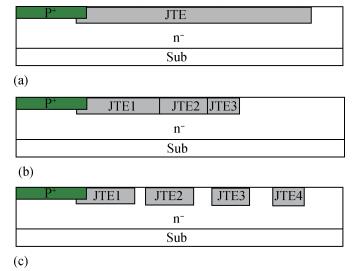
Fig. 1.
Schematic cross-section of (a) S-JTE, (b) M-JTE, and (c) SM-JTE.
SEMICONDUCTOR DEVICES
Tongtong Yang, Song Bai and Runhua Huang
Corresponding author: Yang Tongtong, Email: yangtongtong2010@163.com
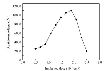
Abstract: Numerical simulations on the optimization of junction termination extension (JTE) have been performed. Various termination techniques have been applied and simulated in this paper, such as single-zone JTE (S-JTE), multi-zone JTE (M-JTE), and space-modulated JTE (SM-JTE). A completely novel and efficient method is demonstrated in this paper to determine total length of SM-JTE, and it is verified through simulation results. The simulation results show that the SM-JTE could provide a protection efficiency (defined in Section 2) of 95.2%, which is much higher than that of M-JTE (82.4%) and S-JTE (64.7%). Based on the fabricated MOSFETs, the interface charge density is extracted and the approximate range of charge density has been determined. The influences of different interface charge densities have been investigated for the three termination techniques respectively. According to the previous reports, the JTE is quite sensitive to the implanted dose, so the blocking capability of each termination structure with different implanted doses is also simulated. The results show that when interface charge is considered, the SM-JTE always shows an enormous advantage over the other two junction termination structures, however the interface charge densities varied. The space-modulated JTE is also applicable to the power planar devices such as MOSFETs and IGBTs, which would provide a very promising lower fabrication cost.
Keywords: 4H-SiC, junction termination extension, interface charge, TCAD
| [1] |
Feng G, Suda J, Kimoto T. Space-modulated junction termination extension for ultrahigh-voltage p-i-n diodes in 4H-SiC. IEEE Trans Electron Devices, 2012, 59: 414 doi: 10.1109/TED.2011.2175486
|
| [2] |
Niwa H, Feng G, Suda J, et al. Breakdown characteristics of 12-20 kV-class 4H-SiC PiN diodes width improved junction termination structures. 24th International Symposium on Power Semiconductor Devices and ICs (ISPSD), 2012: 381
|
| [3] |
Hiyoshi T, Hori T, Suda J, et al. Simulation and experimental study on the junction termination structure for high-voltage 4H-SiC PiN diodes. IEEE Trans Electron Devices, 2008, 55: 1841 doi: 10.1109/TED.2008.926643
|
| [4] |
Singh R, Irvine K G, Capell D C, et al. Large area, ultra-high voltage 4H-SiC p-i-n rectifiers. IEEE Trans Electron Devices, 2002, 49: 2308 doi: 10.1109/TED.2002.805576
|
| [5] |
Nguyen D M, Huang R, Phung L V, et al. Edge termination design improvements for 10 kV 4H-SiC bipolar diodes. Mater Sci Forum, 2013, 609: 740 https://www.researchgate.net/publication/271979235_Edge_Termination_Design_Improvements_for_10_kV_4H-SiC_Bipolar_Diodes
|
| [6] |
Huang R H, Tao Y H, Chen G. Simulation, fabrication and characterization of 6500 V 4H-SiC JBS diode. Adv Mater Res, 2014, 737: 846 http://www.scientific.net/amr.846-847.737.pdf
|
| [7] |
Jayant B B. Analysis of a high-voltage merged p-i-n/Schottky (MPS) rectifier. IEEE Electron Device Lett, 1987, 8(9): 407 doi: 10.1109/EDL.1987.26676
|
| [8] |
Millan J, Godignon P. Wide band-gap power semiconductor devices. Spanish Conference on Electron Devices (CDE), 2013: 293 https://arpa-e-foa.energy.gov/FileContent.aspx?FileID=f7df5ea3-c08b-4dcc-9860-4cb01ca13c76
|
| [9] |
Li Y, Zhao Z F, Li Z H. Epitaxial growth of SiC epilayers for 10 kV Schottky diodes using chloride-based CVD. Adv Mater Res, 2014, 462: 887 https://www.researchgate.net/publication/272615307_Epitaxial_Growth_of_SiC_Epilayers_for_10kV_Schottky_Diodes_using_Chloride-based_CVD
|
| [10] |
Dhar S, Ahyi A C, Williams J R, et al. Temperature dependence of inversion layer carrier concentration and hall mobility in 4H-SiC MOSFETs. Mater Sci Forum, 2012, 713: 717 https://www.researchgate.net/publication/269389178_Temperature_Dependence_of_Inversion_Layer_Carrier_Concentration_and_Hall_Mobility_in_4H-SiC_MOSFETs
|
| [11] |
Ryu S H, Krishnaswami S, Hull B, et al. 10 kV, 5 A 4H-SiC power DMOSFET. Proceeding of the 18th International Symposium on Power Semiconductor Devices & IC's, Naples, Italy, 2006
|
| [12] |
Jiang H P, Ke M L, Sharma Y, et al. Optimum design of 4H-SiC junction barrier Schottky diode with consideration of the anisotropic impact ionization. Mater Sci Forum, 2015, 858: 745 http://www.scientific.net/keyword/Junction_Barrier_Schottky_JBS_Diode/5
|
| [13] |
Kim K H, Kang Y H, Lee J H, et al. Study of 4H-SiC junction barrier Schottky (JBS) diode using various junction structures. Mater Sci Forum, 2015, 858: 733 http://www.scientific.net/keyword/Junction_Barrier_Schottky_JBS_Diode/6
|
| [14] |
Sharma R K, Hazdra P, Popelka S, et al. Optimization of 1700 V 4H-SiC JBS diode parameters. Mater Sci Forum, 2015, 858: 782 https://www.researchgate.net/publication/261046331_Optimization_of_4H-SiC_power_Schottky_Barrier_Diodes
|
| [15] |
Tsuji T, Shiomi H, Ohse N, et al. 3300 V-class 4H SiC implantation-epitaxial MOSFETs with low specific on-resistance of 11.6 mΩ·cm2 and high avalanche withstanding capability. Mater Sci Forum, 2015, 858: 962
|
| [16] |
Elahipanah H, Salemi A, Zetterling C M, et al. Modification of etched junction termination extension for the high voltage 4H-SiC power devices. Mater Sci Forum, 2015, 858: 978 https://www.scientific.net/MSF.858.978
|
| [17] |
TCAD Atlas' Manual www.silvaco.com
|
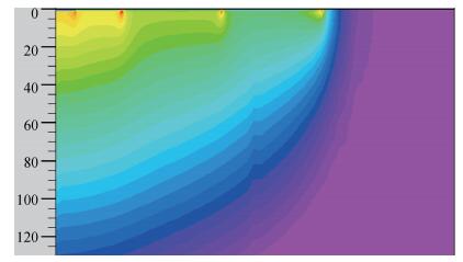
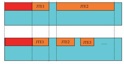
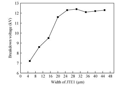
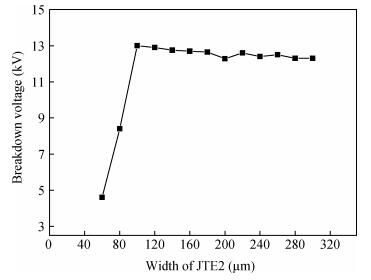
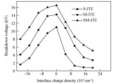
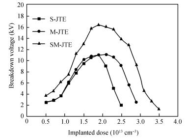
Table 1. Simulated results for multi-zone JTE.

|
| [1] |
Feng G, Suda J, Kimoto T. Space-modulated junction termination extension for ultrahigh-voltage p-i-n diodes in 4H-SiC. IEEE Trans Electron Devices, 2012, 59: 414 doi: 10.1109/TED.2011.2175486
|
| [2] |
Niwa H, Feng G, Suda J, et al. Breakdown characteristics of 12-20 kV-class 4H-SiC PiN diodes width improved junction termination structures. 24th International Symposium on Power Semiconductor Devices and ICs (ISPSD), 2012: 381
|
| [3] |
Hiyoshi T, Hori T, Suda J, et al. Simulation and experimental study on the junction termination structure for high-voltage 4H-SiC PiN diodes. IEEE Trans Electron Devices, 2008, 55: 1841 doi: 10.1109/TED.2008.926643
|
| [4] |
Singh R, Irvine K G, Capell D C, et al. Large area, ultra-high voltage 4H-SiC p-i-n rectifiers. IEEE Trans Electron Devices, 2002, 49: 2308 doi: 10.1109/TED.2002.805576
|
| [5] |
Nguyen D M, Huang R, Phung L V, et al. Edge termination design improvements for 10 kV 4H-SiC bipolar diodes. Mater Sci Forum, 2013, 609: 740 https://www.researchgate.net/publication/271979235_Edge_Termination_Design_Improvements_for_10_kV_4H-SiC_Bipolar_Diodes
|
| [6] |
Huang R H, Tao Y H, Chen G. Simulation, fabrication and characterization of 6500 V 4H-SiC JBS diode. Adv Mater Res, 2014, 737: 846 http://www.scientific.net/amr.846-847.737.pdf
|
| [7] |
Jayant B B. Analysis of a high-voltage merged p-i-n/Schottky (MPS) rectifier. IEEE Electron Device Lett, 1987, 8(9): 407 doi: 10.1109/EDL.1987.26676
|
| [8] |
Millan J, Godignon P. Wide band-gap power semiconductor devices. Spanish Conference on Electron Devices (CDE), 2013: 293 https://arpa-e-foa.energy.gov/FileContent.aspx?FileID=f7df5ea3-c08b-4dcc-9860-4cb01ca13c76
|
| [9] |
Li Y, Zhao Z F, Li Z H. Epitaxial growth of SiC epilayers for 10 kV Schottky diodes using chloride-based CVD. Adv Mater Res, 2014, 462: 887 https://www.researchgate.net/publication/272615307_Epitaxial_Growth_of_SiC_Epilayers_for_10kV_Schottky_Diodes_using_Chloride-based_CVD
|
| [10] |
Dhar S, Ahyi A C, Williams J R, et al. Temperature dependence of inversion layer carrier concentration and hall mobility in 4H-SiC MOSFETs. Mater Sci Forum, 2012, 713: 717 https://www.researchgate.net/publication/269389178_Temperature_Dependence_of_Inversion_Layer_Carrier_Concentration_and_Hall_Mobility_in_4H-SiC_MOSFETs
|
| [11] |
Ryu S H, Krishnaswami S, Hull B, et al. 10 kV, 5 A 4H-SiC power DMOSFET. Proceeding of the 18th International Symposium on Power Semiconductor Devices & IC's, Naples, Italy, 2006
|
| [12] |
Jiang H P, Ke M L, Sharma Y, et al. Optimum design of 4H-SiC junction barrier Schottky diode with consideration of the anisotropic impact ionization. Mater Sci Forum, 2015, 858: 745 http://www.scientific.net/keyword/Junction_Barrier_Schottky_JBS_Diode/5
|
| [13] |
Kim K H, Kang Y H, Lee J H, et al. Study of 4H-SiC junction barrier Schottky (JBS) diode using various junction structures. Mater Sci Forum, 2015, 858: 733 http://www.scientific.net/keyword/Junction_Barrier_Schottky_JBS_Diode/6
|
| [14] |
Sharma R K, Hazdra P, Popelka S, et al. Optimization of 1700 V 4H-SiC JBS diode parameters. Mater Sci Forum, 2015, 858: 782 https://www.researchgate.net/publication/261046331_Optimization_of_4H-SiC_power_Schottky_Barrier_Diodes
|
| [15] |
Tsuji T, Shiomi H, Ohse N, et al. 3300 V-class 4H SiC implantation-epitaxial MOSFETs with low specific on-resistance of 11.6 mΩ·cm2 and high avalanche withstanding capability. Mater Sci Forum, 2015, 858: 962
|
| [16] |
Elahipanah H, Salemi A, Zetterling C M, et al. Modification of etched junction termination extension for the high voltage 4H-SiC power devices. Mater Sci Forum, 2015, 858: 978 https://www.scientific.net/MSF.858.978
|
| [17] |
TCAD Atlas' Manual www.silvaco.com
|


Article views: 5387 Times PDF downloads: 179 Times Cited by: 0 Times
Received: 05 August 2016 Revised: 18 September 2016 Online: Published: 01 April 2017
| Citation: |
Tongtong Yang, Song Bai, Runhua Huang. Optimization of junction termination extension for ultrahigh voltage 4H-SiC planar power devices[J]. Journal of Semiconductors, 2017, 38(4): 044004. doi: 10.1088/1674-4926/38/4/044004
****
T T Yang, S Bai, R H Huang. Optimization of junction termination extension for ultrahigh voltage 4H-SiC planar power devices[J]. J. Semicond., 2017, 38(4): 044004. doi: 10.1088/1674-4926/38/4/044004.

|
| [1] |
Feng G, Suda J, Kimoto T. Space-modulated junction termination extension for ultrahigh-voltage p-i-n diodes in 4H-SiC. IEEE Trans Electron Devices, 2012, 59: 414 doi: 10.1109/TED.2011.2175486
|
| [2] |
Niwa H, Feng G, Suda J, et al. Breakdown characteristics of 12-20 kV-class 4H-SiC PiN diodes width improved junction termination structures. 24th International Symposium on Power Semiconductor Devices and ICs (ISPSD), 2012: 381
|
| [3] |
Hiyoshi T, Hori T, Suda J, et al. Simulation and experimental study on the junction termination structure for high-voltage 4H-SiC PiN diodes. IEEE Trans Electron Devices, 2008, 55: 1841 doi: 10.1109/TED.2008.926643
|
| [4] |
Singh R, Irvine K G, Capell D C, et al. Large area, ultra-high voltage 4H-SiC p-i-n rectifiers. IEEE Trans Electron Devices, 2002, 49: 2308 doi: 10.1109/TED.2002.805576
|
| [5] |
Nguyen D M, Huang R, Phung L V, et al. Edge termination design improvements for 10 kV 4H-SiC bipolar diodes. Mater Sci Forum, 2013, 609: 740 https://www.researchgate.net/publication/271979235_Edge_Termination_Design_Improvements_for_10_kV_4H-SiC_Bipolar_Diodes
|
| [6] |
Huang R H, Tao Y H, Chen G. Simulation, fabrication and characterization of 6500 V 4H-SiC JBS diode. Adv Mater Res, 2014, 737: 846 http://www.scientific.net/amr.846-847.737.pdf
|
| [7] |
Jayant B B. Analysis of a high-voltage merged p-i-n/Schottky (MPS) rectifier. IEEE Electron Device Lett, 1987, 8(9): 407 doi: 10.1109/EDL.1987.26676
|
| [8] |
Millan J, Godignon P. Wide band-gap power semiconductor devices. Spanish Conference on Electron Devices (CDE), 2013: 293 https://arpa-e-foa.energy.gov/FileContent.aspx?FileID=f7df5ea3-c08b-4dcc-9860-4cb01ca13c76
|
| [9] |
Li Y, Zhao Z F, Li Z H. Epitaxial growth of SiC epilayers for 10 kV Schottky diodes using chloride-based CVD. Adv Mater Res, 2014, 462: 887 https://www.researchgate.net/publication/272615307_Epitaxial_Growth_of_SiC_Epilayers_for_10kV_Schottky_Diodes_using_Chloride-based_CVD
|
| [10] |
Dhar S, Ahyi A C, Williams J R, et al. Temperature dependence of inversion layer carrier concentration and hall mobility in 4H-SiC MOSFETs. Mater Sci Forum, 2012, 713: 717 https://www.researchgate.net/publication/269389178_Temperature_Dependence_of_Inversion_Layer_Carrier_Concentration_and_Hall_Mobility_in_4H-SiC_MOSFETs
|
| [11] |
Ryu S H, Krishnaswami S, Hull B, et al. 10 kV, 5 A 4H-SiC power DMOSFET. Proceeding of the 18th International Symposium on Power Semiconductor Devices & IC's, Naples, Italy, 2006
|
| [12] |
Jiang H P, Ke M L, Sharma Y, et al. Optimum design of 4H-SiC junction barrier Schottky diode with consideration of the anisotropic impact ionization. Mater Sci Forum, 2015, 858: 745 http://www.scientific.net/keyword/Junction_Barrier_Schottky_JBS_Diode/5
|
| [13] |
Kim K H, Kang Y H, Lee J H, et al. Study of 4H-SiC junction barrier Schottky (JBS) diode using various junction structures. Mater Sci Forum, 2015, 858: 733 http://www.scientific.net/keyword/Junction_Barrier_Schottky_JBS_Diode/6
|
| [14] |
Sharma R K, Hazdra P, Popelka S, et al. Optimization of 1700 V 4H-SiC JBS diode parameters. Mater Sci Forum, 2015, 858: 782 https://www.researchgate.net/publication/261046331_Optimization_of_4H-SiC_power_Schottky_Barrier_Diodes
|
| [15] |
Tsuji T, Shiomi H, Ohse N, et al. 3300 V-class 4H SiC implantation-epitaxial MOSFETs with low specific on-resistance of 11.6 mΩ·cm2 and high avalanche withstanding capability. Mater Sci Forum, 2015, 858: 962
|
| [16] |
Elahipanah H, Salemi A, Zetterling C M, et al. Modification of etched junction termination extension for the high voltage 4H-SiC power devices. Mater Sci Forum, 2015, 858: 978 https://www.scientific.net/MSF.858.978
|
| [17] |
TCAD Atlas' Manual www.silvaco.com
|

 WeChat ID
Journal of Semiconductors © 2017 All Rights Reserved 京ICP备05085259号-2

 DownLoad: