


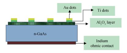
Fig. 1.
(Color online) Schematic model of the Au/Ti/Al2O3/n-GaAs structure
SEMICONDUCTOR DEVICES
Abdulkerim Karabulut1, , Hasan Efeoglu2 and Abdulmecit Turut3
Corresponding author: Abdulkerim Karabulut, Email: akerimkara@gmail.com
Abstract: The Au/Ti/n-GaAs structures with and without Al2O3 interfacial layer have been fabricated.The Al2O3 interfacial layer has been formed on the GaAs substrate by atomic layer deposition.The effects of the interfacial layer on the current-voltage (I-V) and capacitance-voltage (C-V) characteristics of the devices have been investigated in the temperature range of 60-300 K.It has been seen that the carrier concentration from C-V characteristics for the MIS (metal/insulating layer/semiconductor) diode with Al2O3 interfacial layer has a higher value than that for the reference diode without the Al2O3 interfacial layer (MS).Such a difference in the doping concentration has been attributed not to doping variation in the semiconductor bulk but to the presence of the Al2O3 interfacial layer because both diodes have been made on the pieces cut from the same n-type GaAs wafer.The temperaturedependent I-V characteristics of the MIS diode do not obey the thermionic emission current theory because of the presence of the Al2O3 layer.An electron tunneling factor, aδ (χ)1/2, value of 20.64 has been found from the I-V-T data of the MIS diode.An average value of 0.627 eV for the mean tunneling barrier height, χ, presented by the Al2O3 layer has been obtained.
Keywords: metal-insulating layer-semiconductor contacts, atomic layer deposition, Schottky diodes, barrier inhomogeneity
| [1] |
Rhoderick E H, Williams R H. Metal-semiconductor contacts. 2nd ed. Oxford: Clerandon Press, 1988
|
| [2] |
Sze S M. Physics of semiconductor devices. 2nd ed. New York: John Willey, 1981
|
| [3] |
Mönch W. Semiconductor surfaces and interfaces. 2nd ed. Berlin: Springer, 1995
|
| [4] |
Ashok S, Borrego J M, Gudmann R J. Electrical characteristics of GaAs MIS Schottky diodes. Solid-State Electron, 1979, 22(7): 621 doi: 10.1016/0038-1101(79)90135-7
|
| [5] |
Xu Y, Cheng C, Du S, et al. Contacts between two-and threedimensional materials: ohmic, Schottky, and p-n heterojunctions. ACS Nano, 2016, 10: 4895 doi: 10.1021/acsnano.6b01842
|
| [6] |
Asubay S, Genisel M F, Ocak Y S. Electrical parameters of a DC sputtered Mo/n-type 6H-SiC Schottky barrier diode. Mater Sci Semicond Process, 2014, 28: 94 doi: 10.1016/j.mssp.2014.07.003
|
| [7] |
Mönch W. On the band-structure lineup at Schottky contacts and semiconductor heterostructures. Mater Sci Semicond Process, 2014, 28: 2 doi: 10.1016/j.mssp.2014.03.024
|
| [8] |
Türüt A, BatıB, Kökçe A, et al. The bias-dependence change of barrier height of Schottky diodes under forward bias by including the series resistance effect. Phys Scr, 1996, 53: 118 doi: 10.1088/0031-8949/53/1/023
|
| [9] |
Card H C, Rhoderick E H. Studies of tunnel MOS diodesⅡ. Thermal equilibrium considerations. J Phys D: Appl Phys, 1971, 4: 1589 doi: 10.1088/0022-3727/4/10/319
|
| [10] |
Alialy S, Kaya A, Marıl E, et al. Electronic transport of Au/(Ca1.9Pr0.1Co4Ox/n-Si structures analyzed over a wide temperature range. Philosophical Mag, 2015, 95: 1448 doi: 10.1080/14786435.2015.1033029
|
| [11] |
Biber M, Temirci C, Turut A. Barrier height enhancement in the Au/N-GaAs Schottky diodes with anodization process. J Vac Sci Technol B, 2002, 20: 11 https://www.researchgate.net/publication/224467881_Barrier_height_enhancement_in_the_Aun-GaAs_Schottky_diodes_with_anodization_process
|
| [12] |
Marıl E, Kaya A, Çetinkaya H G. On the temperature dependent forward bias current-voltage (I-V) characteristics in Au/2% graphene-cobalt doped (Ca3Co4Ga0.001Ox//n-Si structure. Mater Sci Semicond Process, 2015, 39: 332 doi: 10.1016/j.mssp.2015.05.029
|
| [13] |
Dhibi O, Ltaief A, Chaaben N, et al. Effect of thin gold interlayer on the electrical and dielectrical behaviors of ITO/MEH-PPV/Al structures. Microelectron Eng, 2014, 129: 24 doi: 10.1016/j.mee.2014.06.021
|
| [14] |
Reddy M S P, Puneetha P, Reddy V R, et al. Temperaturedependent electrical properties and carrier transport mechanisms of TMAH-treated Ni/Au/Al2O3/GaN MIS diode. J Electron Mater, 2016, 45(11): 5655 doi: 10.1007/s11664-016-4809-6
|
| [15] |
Turut A, Karabulut A, Ejderha K, et al. Capacitanceconductance-current-voltage characteristics of atomic layer deposited Au/Ti/Al2O3/n-GaAs MIS structures. Mater Sci Semicond Process, 2015, 39: 400 doi: 10.1016/j.mssp.2015.05.025
|
| [16] |
Turut A, Karabulut A, Ejderha K, et al. Capacitance-conductance characteristics of Au/Ti/Al2O3/n-GaAs structures with very thin Al2O3 interfacial layer. Mater Res Express, 2015, 2: 046301 doi: 10.1088/2053-1591/2/4/046301
|
| [17] |
Wilk G D, Wallace R M, Anthony J M. High-k gate dielectrics: current status and materials properties considerations. J Appl Phys, 2001, 89(10): 5243 doi: 10.1063/1.1361065
|
| [18] |
Sayan S, Bartynski R A, Zhao X, et al. Valence and conduction band offsets of a ZrO2/SiOxNy/n-Si CMOS gate stack: a combined photoemission and inverse photoemission study. Phys Stat Sol B, 2004, 241(10): 2246 doi: 10.1002/(ISSN)1521-3951
|
| [19] |
Cheong K Y, Moon J H, Kim H J, et al. Current conduction mechanisms in atomic-layer-deposited HfO2/nitrided SiO2HfO2/nitrided SiO2 stacked gate on 4H silicon carbide. J Appl Phys, 2008, 103(8): 084113 doi: 10.1063/1.2908870
|
| [20] |
Luo X, Rahbarihagh Y, Hwang J C M, et al. Temporal and thermal stability of Al2O3-passivated phosphorene MOSFETs. IEEE Electron Device Lett, 2014, 35(12): 1314 doi: 10.1109/LED.2014.2362841
|
| [21] |
Chagarov E A, Kummel A C. Density functional theory simulations of amorphous high-k oxides on a compound semiconductor alloy: a-Al2O3/InGaAs (100)-(4×2), a-HfO2/InGaAs (100)-(4×2), and a-ZrO2/InGaAs (100)-(4×2). J Chem Phys, 2011, 135: 244705 doi: 10.1063/1.3657439
|
| [22] |
Chang Y H, Huang M L, Chang P, et al. Electrical properties and interfacial chemical environments of in-situ atomic layer deposited Al2O3 on freshly molecular beam epitaxy grown GaAs. Microelectron Eng, 2011, 88: 440 doi: 10.1016/j.mee.2010.09.015
|
| [23] |
Hinkle C L, Milojevic M, Brennan B, et al. Detection of Ga suboxides and their impact onⅡ-Ⅴ passivation and Fermi-level pinning. Appl Phys Lett, 2009, 94: 162101 doi: 10.1063/1.3120546
|
| [24] |
Wu Y Q, Ye P D, Wilk G D, et al. GaN metal-oxidesemiconductor field-effect-transistor with atomic layer deposited Al2O3 as gate dielectric. Mater Sci Eng B, 2006, 135: 282 doi: 10.1016/j.mseb.2006.08.020
|
| [25] |
Kukli K, Ritala M, Sajavaara T, et al. Comparison of hafnium oxide films grown by atomic layer deposition from iodide and chloride precursors. Thin Solid Films, 2002, 416: 72 doi: 10.1016/S0040-6090(02)00612-0
|
| [26] |
Ali A, Madan H, Koveshnikov S, et al. Small signal response of inversion layers in high mobility In0.53Ga0.47As MOSFETs made with thin high-k dielectrics. IEEE Trans Electron Devices, 2010, 57(4): 742 doi: 10.1109/TED.2010.2041855
|
| [27] |
Chobpattana V, Mates T E, Mitchell W J, et al. Influence of plasma-based in-situ surface cleaning procedures on HfO2/In0.53Ga0.47As gate stack properties. J Appl Phys, 2013, 114: 154108 doi: 10.1063/1.4825259
|
| [28] |
Chobpattana V, Mikheev E, Zhang J Y, et al. Extremely scaled high-k/In0.53Ga0.47As gate stacks with low leakage and low interface trap densities. J Appl Phys, 2014, 116: 124104 doi: 10.1063/1.4896494
|
| [29] |
Huang C Y, Lee S, Cohen-Elias D, et al. Reduction of leakage current in In0.53Ga0.47As channel metal-oxide-semiconductor field-effect-transistors using AlAs0.56Sb0.44confinement layers. Appl Phys Lett, 2013, 103: 203502 doi: 10.1063/1.4831683
|
| [30] |
Stemmer S, Chobpattana V, Rajan S. Frequency dispersion inⅡ-Ⅴ metal-oxide-semiconductor capacitors. Appl Phys Lett, 2012, 100: 233510 doi: 10.1063/1.4724330
|
| [31] |
Xu M, Wu Y Q, Koybasi O, et al. Metal-oxide-semiconductor field-effect transistors on GaAs (111) A surface with atomiclayer-deposited AlO as gate dielectrics. Appl Phys Lett, 2009, 94: 212104 doi: 10.1063/1.3147218
|
| [32] |
Afanas'ev V V, Stesmans A, Brammertz G, et al. Energy barriers at interfaces between (100) InxGa1-xAs (0≤ x≤ 60:53) and atomic-layer deposited Al2O3 and HfO2. Appl Phys Lett, 2009, 94: 202110 doi: 10.1063/1.3137187
|
| [33] |
Wu Y Q, Xu M, Ye P D, et al. Atomic-layer-deposited Al2O3/GaAs metal-oxide-semiconductor field-effect transistor on Si substrate using aspect ratio trapping technique. Appl Phys Lett, 2008, 93: 242106 doi: 10.1063/1.3050466
|
| [34] |
Chou H Y, O'Connor E, Hurley P K, et al. Interface barriers at the interfaces of polar GaAs (111) faces with Al2O3. Appl Phys Lett, 2012, 100: 141602 doi: 10.1063/1.3698461
|
| [35] |
Dong L, Wang X W, Zhang J Y, et al. GaAs enhancement-mode NMOSFETs enabled by atomic layer epitaxial La1.8Y0.2O3 as dielectric. IEEE Electron Lett, 2013, 34(4): 487 doi: 10.1109/LED.2013.2244058
|
| [36] |
Sun X, Ma T P. Electrical characterization of gate traps in FETs with Ge and Ⅱ-Ⅴ channels. IEEE Trans Device Mater Reliab, 2013, 13(4): 463 doi: 10.1109/TDMR.2013.2276755
|
| [37] |
Huang M L, Chang Y C, Chang Y H, et al. Energy-band parameters of atomic layer deposited Al2O3 and HfO2 on InxGa1-xAs. Appl Phys Lett, 2009, 94: 052106 doi: 10.1063/1.3078399
|
| [38] |
Nguyen N V, Kirillov O A, Jiang W, et al. Band offsets of atomiclayer-deposited Al2O3 on GaAs and the effects of surface treatment. Appl Phys Lett, 2008, 93: 082105 doi: 10.1063/1.2976676
|
| [39] |
Xuan Y, Lin H C, Ye P D. Simplified surface preparation for GaAs passivation using atomic layer deposited high-k dielectrics. IEEE Trans Electron Devices, 2007, 54: 1811 doi: 10.1109/TED.2007.900678
|
| [40] |
Chou H Y, Afanas'ev V V, Houssa M, et al. Electron band alignment at the interface of (100) InSb with atomic-layer-deposited Al2O3. Appl Phys Lett, 2012, 101: 082114 doi: 10.1063/1.4747797
|
| [41] |
Peng J J, Song C, Cui B, et al. Manipulation of orbital occupancy by ferroelectric polarization in LaNiO3/BaTiO3-δ heterostructures. Appl Phys Lett, 2015, 107: 182904 doi: 10.1063/1.4935214
|
| [42] |
Peng J J, Song C, Li F, et al. Charge transfer and orbital reconstruction in strain-engineered (La, Sr) MnO3/LaNiO3 heterostructures. ACS Appl Mater Interfaces, 2015, 7: 17700 doi: 10.1021/acsami.5b04994
|
| [43] |
Altuntas H, Akgun C O, Donmez I, et al. Current transport mechanisms in plasma-enhanced atomic layer deposited AlN thin films. J Appl Phys, 2015, 117: 155101 doi: 10.1063/1.4917567
|
| [44] |
Van Den Berghe L M O, Van Meirhaeghe R L, Laflere W H, et al. On the electrical properties, the interfacial reactivity and the thermal stability of CoSi2/TiSi2/Co and Ti/p-InP Schottky barriers. Solid-State Electron, 1990, 33: 79 doi: 10.1016/0038-1101(90)90013-5
|
| [45] |
Donoval D, Barus M, Zdimal M. Analysis of I-V measurements on Pt/Si-Si Schottky structures in a wide temperature range. Solid-State Electron, 1991, 34: 1365 doi: 10.1016/0038-1101(91)90031-S
|
| [46] |
Venter A, Murape D M, Botha J R, et al. Transport characteristics of Pd Schottky barrier diodes on epitaxial n-GaSb as determined from temperature dependent current-voltage measurements. Thin Solid Films, 2015, 574: 32 doi: 10.1016/j.tsf.2014.11.057
|
| [47] |
Mohammad S N. Contact mechanisms and design principles for Schottky contacts to group-Ⅱ nitrides. J Appl Phys, 2005, 97: 063703 doi: 10.1063/1.1856226
|
| [48] |
Osvald J. Numerical study of electrical transport in inhomogeneous Schottky diodes. J Appl Phys, 1999, 85: 1935 doi: 10.1063/1.369185
|
| [49] |
Kumar A A, Rao L D, Reddy V R, et al. Analysis of electrical characteristics of Er/p-InP Schottky diode at high temperature range. Curr Appl Phys, 2013, 13: 975 doi: 10.1016/j.cap.2013.01.046
|
| [50] |
Ahmad Z, Sayyad M H. Extraction of electronic parameters of Schottky diode based on an organic semiconductor methylred. Physica E, 2009, 41: 631 doi: 10.1016/j.physe.2008.08.068
|
| [51] |
Korucu D, Duman S. Current-voltage-temperature characteristics of Au/p-InP Schottky barrier diode. Thin Solid Films, 2013, 531: 436 doi: 10.1016/j.tsf.2013.01.079
|
| [52] |
El-Menyawy E M. Electrical and photovoltaic properties of Gaussian distributed inhomogeneous barrier based on tris (8-hydroxyquinoline) indium/p-Si interface. Mater Sci Semicond Process, 2015, 32: 145 doi: 10.1016/j.mssp.2015.01.017
|
| [53] |
Osvald J, Horvath Z J. Theoretical study of the temperature dependence of electrical characteristics of Schottky diodes with an inverse near-surface layer. Appl Surf Sci, 2014, 234: 349 http://www.sciencedirect.com/science/article/pii/S0169433204006488
|
| [54] |
Ouennoughi Z, Toumi S, Weiss R. Study of barrier inhomogeneities using I-V-T characteristics of Mo/4H-SiC Schottky diode. Physica B, 2015, 456: 176 doi: 10.1016/j.physb.2014.08.031
|
| [55] |
El-Menyawy E M, Ashery A. Current-voltage characteristics and inhomogeneous barrier height analysis of Au/poly (otoluidine)/ p-Si/Al heterojunction diode. J Mater Sci, 2014, 25: 3939 https://www.researchgate.net/publication/272018428_Current-voltage_characteristics_and_inhomogeneous_barrier_height_analysis_of_Aupolyo-toluidinep-SiAl_heterojunction_diode
|
| [56] |
Tung R T. Electron transport at metal-semiconductor interfaces: general theory. Phys Rev B, 1992, 45: 13510 https://www.researchgate.net/publication/13288910_Electron_transport_at_metal-semiconductor_interfaces_General_theory
|
| [57] |
Sullivan J P, Tung R T, Pinto M R, et al. Electron transport of inhomogeneous Schottky barriers: a numerical study. J Appl Phys, 1991, 70: 7403 doi: 10.1063/1.349737
|
| [58] |
Tung R T. The physics and chemistry of the Schottky barrierheight. Appl Phys Rev, 2014, 1: 011304 doi: 10.1063/1.4858400
|
| [59] |
Gammon P M, Péerez-Tomás A, Shah V A, et al. Modelling the inhomogeneous SiC Schottky interface. J Appl Phys, 2013, 114: 223704 doi: 10.1063/1.4842096
|
| [60] |
Dogan H, Yıldırım N, Turut A, et al. Determination of the characteristic parameters of Sn/n-GaAs/Al-Ge Schottky diodes by a barrier height inhomogeneity model. Semicond Sci Technol, 2006, 21: 822 doi: 10.1088/0268-1242/21/6/021
|
| [61] |
Ejderha K, Yıldırım N, Turut A. Temperature-dependent currentvoltage characteristics in thermally annealed ferromagnetic Co/n-GaN Schottky contacts. Eur Phys J Appl Phys, 2014, 68: 20101 doi: 10.1051/epjap/2014140200
|
| [62] |
Gülnahar M, Karacali T, Efeoglu H. Porous Si based Al Schottky structures on p+-Si: a possible way for nano Schottky fabrication. Electrochimica Acta, 2015, 168: 41 doi: 10.1016/j.electacta.2015.03.204
|
| [63] |
Korucu D, Turut A, Efeoglu H. Temperature dependent I-V characteristics of an Au/n-GaAs Schottky diode analyzed using Tung's model. Physica B, 2013, 414: 35 doi: 10.1016/j.physb.2013.01.010
|
| [64] |
Dobrocka E, Osvald J. Influence of barrier height distribution on the parameters of Schottky diodes. Appl Phys Lett, 1994, 65: 575 doi: 10.1063/1.112300
|
| [65] |
Biyikli N, Karabulut A, Efegolu H, et al. Electrical characteristics of Au/Ti/n-GaAs contacts over a wide measurement temperature range. Phys Scr, 2014, 89: 095804 doi: 10.1088/0031-8949/89/9/095804
|
| [66] |
Güzeldir B, Sağlam M. Temperature dependent electrical properties of Cd/CdS/n-Si/Au-Sb structures. Mater Sci Semicond Process, 2015, 30: 658 doi: 10.1016/j.mssp.2014.09.020
|
| [67] |
Roul B, Mukundan S, Chandan G, et al. Barrier height inhomogeneity in electrical transport characteristics of InGaN/GaN heterostructure interfaces. AIP Adv, 2015, 5: 037130 doi: 10.1063/1.4916264
|
| [68] |
Song Y P, Van Meirhaeghe R L, Laflére W H, et al. On the difference in apparent barrier height as obtained from capacitance-voltage and current-voltage-temperature measurements on Al/p-InP Schottky barriers. Solid-State Electron, 1986, 29: 633 doi: 10.1016/0038-1101(86)90145-0
|
| [69] |
Werner J H, Guttler H H. Barrier inhomogeneities at Schottky contacts. J Appl Phys, 1991, 69: 1522 doi: 10.1063/1.347243
|
| [70] |
Chand S, Kumar J. On the existence of a distribution of barrier heights in Pd2Si/Si Schottky diodes. J Appl Phys, 1996, 80: 288 doi: 10.1063/1.362818
|
| [71] |
Duman S, Ejderha K, Yigit O, et al. Determination of contact parameters of Ni/n-GaP Schottky contacts. Microelectron Reliab, 2012, 52: 1005 doi: 10.1016/j.microrel.2011.12.018
|
| [72] |
Akkaya A, Esmer L, Karaaslan T, et al. Electrical characterization of Ni/Al 0:09 Ga0.91N Schottky barrier diodes as a function of temperature. Mater Sci Semicond Process, 2014, 28: 127 doi: 10.1016/j.mssp.2014.07.053
|
| [73] |
Horvath Z J. Comment on "Analysis of Ⅳ measurements on CrSi2 Si Schottky structures in a wide temperature range". Solid State Electron, 1996, 39: 176 doi: 10.1016/0038-1101(95)00148-M
|
| [74] |
Mayimele M A, Diale M, Mtangi W, et al. Temperaturedependent current-voltage characteristics of Pd/ZnO Schottky barrier diodes and the determination of the Richardson constant. Mater Sci Semicond Process, 2015, 34: 359 doi: 10.1016/j.mssp.2015.02.018
|
| [75] |
Leroy W P, Opsomer K, Forment S, et al. The barrier height inhomogeneity in identically prepared Au/n-GaAs Schottky barrier diodes. Solid State Electron, 2005, 49: 878 doi: 10.1016/j.sse.2005.03.005
|
| [76] |
Efegolu H, Turut A. The current-voltage characteristics of the Au/MBE n-GaAs Schottky diodes in a wide temperature range. Int J Modern Phys B, 2013, 27: 1350088 doi: 10.1142/S0217979213500884
|
| [77] |
Gümüş A, Altındal Ş. Current-transport mechanisms in gold/polypyrrole/n-silicon Schottky barrier diodes in the temperature range of 110-360 K. Mater Sci Semicond Process, 2014, 28: 66 doi: 10.1016/j.mssp.2014.05.060
|
| [78] |
Benamar M, Anani M, Akkal B, et al. Ni/SiC-6H Schottky barrier diode interfacial states characterization related to temperature. J Alloys Comp, 2014, 603: 197 doi: 10.1016/j.jallcom.2014.02.177
|
| [79] |
Steven P, Kowalczyk S P, Waldrop J R, et al. Reactivity and interface chemistry during Schottky-barrier formations: metals on thin native oxides of GaAs investigated by X-ray photoelectron spectroscopy. Appl Phys Lett, 1981, 38: 167 doi: 10.1063/1.92289
|
| [80] |
Ayyildiz E, Turut A. The effect of thermal treatment on the characteristic parameters of Ni/-, Ti/-and NiTi alloy/n-GaAs Schottky diodes. Solid-State Electron, 1999, 43: 521 doi: 10.1016/S0038-1101(98)00287-1
|
| [81] |
Jones F E, Wood B P, Myers J A, et al. Current transport and the role of barrier inhomogeneities at the high barrier n-InP|poly (pyrrole) interface. J Appl Phys, 1999, 86: 6431 doi: 10.1063/1.371707
|
| [82] |
Biber M, Coskun C, Turut A. Current-voltage-temperature analysis of inhomogeneous Au/n-GaAs Schottky contacts. Eur Phys J Appl Phys, 2005, 31: 79 doi: 10.1051/epjap:2005050
|
| [83] |
Elghoul N, Kraiem S, Jemai R, et al. Annealing effects on electrical and optical properties of a-Si:H layer deposited by PECVD. Mater Sci Semicond Process, 2015, 40, 302 doi: 10.1016/j.mssp.2015.06.033
|
| [84] |
Kim H, Jung C Y, Kim S H, et al. A comparative electrical transport study on Cu/n-type InP Schottky diode measured at 300 and 100 K. Current Appl Phys, 2016, 16: 37 doi: 10.1016/j.cap.2015.10.008
|
| [85] |
Altındal S. On the origin of increase in the barrier height and decrease in ideality factor with increase temperature in Ag/SiO2/p-Si (MIS) Schottky barrier diodes (SBDs). J Mater Electron Device, 2015, 1: 42
|
| [86] |
Kavasoglu N, Kavasoglu A S, Metin B. A different approach to solar cell simulation. Mater Res Bull, 2015, 70: 804 doi: 10.1016/j.materresbull.2015.06.007
|
| [87] |
Parihar U, Ray J, Panchal C J, et al. Influence of temperature on Al/p-CuInAlSe2 thin-film Schottky diodes. Appl Phys A, 2016, 122: 568 doi: 10.1007/s00339-016-0105-9
|
| [88] |
Li Y, Fu L, Sun J, et al. Study of barrier height and trap centers of Au/n-Hg3In2Te6 Schottky contacts by current-voltage (Ⅳ) characteristics and deep level transient spectroscopy. J Appl Phys, 2015, 117: 085704 doi: 10.1063/1.4913450
|
| [89] |
Kaufmann I R, Pereira M B, Boudinov H I. Schottky barrier height of Ni/TiO2/4H-SiC metal-insulator-semiconductor diodes. Semicond Sci Technol, 2015, 30(12): 125002 doi: 10.1088/0268-1242/30/12/125002
|
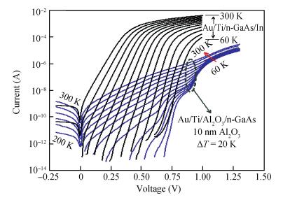
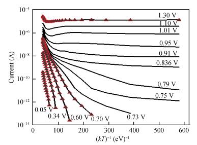
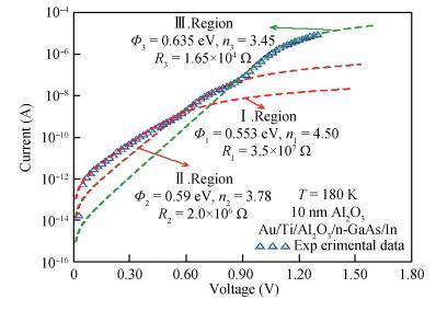
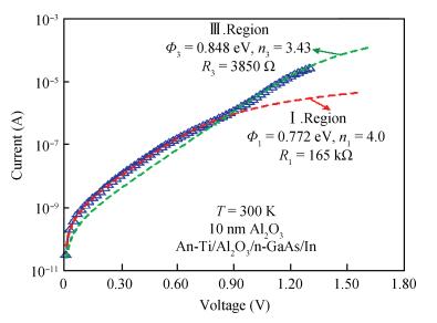
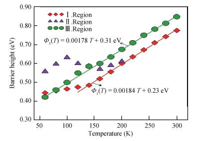
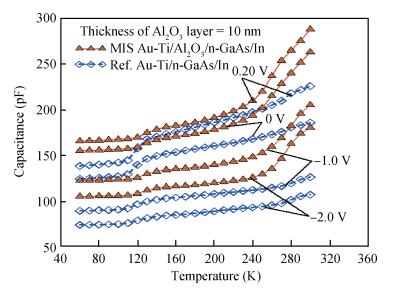
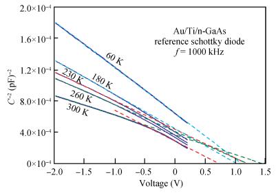
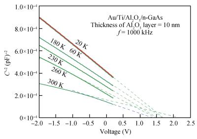
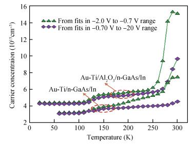
Table 1. Experimental diode parameters from C-2-V characteristics for the reference Au/Ti/n-GaAs and MIS Au/Ti/Al2O3/n-GaAs structures in the temperature range of 60-300 K with steps of 20 K. The data of the Ⅱ. CV region corresponding to (-0.7 V)-(+0.2 V) range in the C-2-V curve at any temperature were given in the table. Vn is the potential difference between Fermi level and the conduction band edge in the neutral region.

|
| [1] |
Rhoderick E H, Williams R H. Metal-semiconductor contacts. 2nd ed. Oxford: Clerandon Press, 1988
|
| [2] |
Sze S M. Physics of semiconductor devices. 2nd ed. New York: John Willey, 1981
|
| [3] |
Mönch W. Semiconductor surfaces and interfaces. 2nd ed. Berlin: Springer, 1995
|
| [4] |
Ashok S, Borrego J M, Gudmann R J. Electrical characteristics of GaAs MIS Schottky diodes. Solid-State Electron, 1979, 22(7): 621 doi: 10.1016/0038-1101(79)90135-7
|
| [5] |
Xu Y, Cheng C, Du S, et al. Contacts between two-and threedimensional materials: ohmic, Schottky, and p-n heterojunctions. ACS Nano, 2016, 10: 4895 doi: 10.1021/acsnano.6b01842
|
| [6] |
Asubay S, Genisel M F, Ocak Y S. Electrical parameters of a DC sputtered Mo/n-type 6H-SiC Schottky barrier diode. Mater Sci Semicond Process, 2014, 28: 94 doi: 10.1016/j.mssp.2014.07.003
|
| [7] |
Mönch W. On the band-structure lineup at Schottky contacts and semiconductor heterostructures. Mater Sci Semicond Process, 2014, 28: 2 doi: 10.1016/j.mssp.2014.03.024
|
| [8] |
Türüt A, BatıB, Kökçe A, et al. The bias-dependence change of barrier height of Schottky diodes under forward bias by including the series resistance effect. Phys Scr, 1996, 53: 118 doi: 10.1088/0031-8949/53/1/023
|
| [9] |
Card H C, Rhoderick E H. Studies of tunnel MOS diodesⅡ. Thermal equilibrium considerations. J Phys D: Appl Phys, 1971, 4: 1589 doi: 10.1088/0022-3727/4/10/319
|
| [10] |
Alialy S, Kaya A, Marıl E, et al. Electronic transport of Au/(Ca1.9Pr0.1Co4Ox/n-Si structures analyzed over a wide temperature range. Philosophical Mag, 2015, 95: 1448 doi: 10.1080/14786435.2015.1033029
|
| [11] |
Biber M, Temirci C, Turut A. Barrier height enhancement in the Au/N-GaAs Schottky diodes with anodization process. J Vac Sci Technol B, 2002, 20: 11 https://www.researchgate.net/publication/224467881_Barrier_height_enhancement_in_the_Aun-GaAs_Schottky_diodes_with_anodization_process
|
| [12] |
Marıl E, Kaya A, Çetinkaya H G. On the temperature dependent forward bias current-voltage (I-V) characteristics in Au/2% graphene-cobalt doped (Ca3Co4Ga0.001Ox//n-Si structure. Mater Sci Semicond Process, 2015, 39: 332 doi: 10.1016/j.mssp.2015.05.029
|
| [13] |
Dhibi O, Ltaief A, Chaaben N, et al. Effect of thin gold interlayer on the electrical and dielectrical behaviors of ITO/MEH-PPV/Al structures. Microelectron Eng, 2014, 129: 24 doi: 10.1016/j.mee.2014.06.021
|
| [14] |
Reddy M S P, Puneetha P, Reddy V R, et al. Temperaturedependent electrical properties and carrier transport mechanisms of TMAH-treated Ni/Au/Al2O3/GaN MIS diode. J Electron Mater, 2016, 45(11): 5655 doi: 10.1007/s11664-016-4809-6
|
| [15] |
Turut A, Karabulut A, Ejderha K, et al. Capacitanceconductance-current-voltage characteristics of atomic layer deposited Au/Ti/Al2O3/n-GaAs MIS structures. Mater Sci Semicond Process, 2015, 39: 400 doi: 10.1016/j.mssp.2015.05.025
|
| [16] |
Turut A, Karabulut A, Ejderha K, et al. Capacitance-conductance characteristics of Au/Ti/Al2O3/n-GaAs structures with very thin Al2O3 interfacial layer. Mater Res Express, 2015, 2: 046301 doi: 10.1088/2053-1591/2/4/046301
|
| [17] |
Wilk G D, Wallace R M, Anthony J M. High-k gate dielectrics: current status and materials properties considerations. J Appl Phys, 2001, 89(10): 5243 doi: 10.1063/1.1361065
|
| [18] |
Sayan S, Bartynski R A, Zhao X, et al. Valence and conduction band offsets of a ZrO2/SiOxNy/n-Si CMOS gate stack: a combined photoemission and inverse photoemission study. Phys Stat Sol B, 2004, 241(10): 2246 doi: 10.1002/(ISSN)1521-3951
|
| [19] |
Cheong K Y, Moon J H, Kim H J, et al. Current conduction mechanisms in atomic-layer-deposited HfO2/nitrided SiO2HfO2/nitrided SiO2 stacked gate on 4H silicon carbide. J Appl Phys, 2008, 103(8): 084113 doi: 10.1063/1.2908870
|
| [20] |
Luo X, Rahbarihagh Y, Hwang J C M, et al. Temporal and thermal stability of Al2O3-passivated phosphorene MOSFETs. IEEE Electron Device Lett, 2014, 35(12): 1314 doi: 10.1109/LED.2014.2362841
|
| [21] |
Chagarov E A, Kummel A C. Density functional theory simulations of amorphous high-k oxides on a compound semiconductor alloy: a-Al2O3/InGaAs (100)-(4×2), a-HfO2/InGaAs (100)-(4×2), and a-ZrO2/InGaAs (100)-(4×2). J Chem Phys, 2011, 135: 244705 doi: 10.1063/1.3657439
|
| [22] |
Chang Y H, Huang M L, Chang P, et al. Electrical properties and interfacial chemical environments of in-situ atomic layer deposited Al2O3 on freshly molecular beam epitaxy grown GaAs. Microelectron Eng, 2011, 88: 440 doi: 10.1016/j.mee.2010.09.015
|
| [23] |
Hinkle C L, Milojevic M, Brennan B, et al. Detection of Ga suboxides and their impact onⅡ-Ⅴ passivation and Fermi-level pinning. Appl Phys Lett, 2009, 94: 162101 doi: 10.1063/1.3120546
|
| [24] |
Wu Y Q, Ye P D, Wilk G D, et al. GaN metal-oxidesemiconductor field-effect-transistor with atomic layer deposited Al2O3 as gate dielectric. Mater Sci Eng B, 2006, 135: 282 doi: 10.1016/j.mseb.2006.08.020
|
| [25] |
Kukli K, Ritala M, Sajavaara T, et al. Comparison of hafnium oxide films grown by atomic layer deposition from iodide and chloride precursors. Thin Solid Films, 2002, 416: 72 doi: 10.1016/S0040-6090(02)00612-0
|
| [26] |
Ali A, Madan H, Koveshnikov S, et al. Small signal response of inversion layers in high mobility In0.53Ga0.47As MOSFETs made with thin high-k dielectrics. IEEE Trans Electron Devices, 2010, 57(4): 742 doi: 10.1109/TED.2010.2041855
|
| [27] |
Chobpattana V, Mates T E, Mitchell W J, et al. Influence of plasma-based in-situ surface cleaning procedures on HfO2/In0.53Ga0.47As gate stack properties. J Appl Phys, 2013, 114: 154108 doi: 10.1063/1.4825259
|
| [28] |
Chobpattana V, Mikheev E, Zhang J Y, et al. Extremely scaled high-k/In0.53Ga0.47As gate stacks with low leakage and low interface trap densities. J Appl Phys, 2014, 116: 124104 doi: 10.1063/1.4896494
|
| [29] |
Huang C Y, Lee S, Cohen-Elias D, et al. Reduction of leakage current in In0.53Ga0.47As channel metal-oxide-semiconductor field-effect-transistors using AlAs0.56Sb0.44confinement layers. Appl Phys Lett, 2013, 103: 203502 doi: 10.1063/1.4831683
|
| [30] |
Stemmer S, Chobpattana V, Rajan S. Frequency dispersion inⅡ-Ⅴ metal-oxide-semiconductor capacitors. Appl Phys Lett, 2012, 100: 233510 doi: 10.1063/1.4724330
|
| [31] |
Xu M, Wu Y Q, Koybasi O, et al. Metal-oxide-semiconductor field-effect transistors on GaAs (111) A surface with atomiclayer-deposited AlO as gate dielectrics. Appl Phys Lett, 2009, 94: 212104 doi: 10.1063/1.3147218
|
| [32] |
Afanas'ev V V, Stesmans A, Brammertz G, et al. Energy barriers at interfaces between (100) InxGa1-xAs (0≤ x≤ 60:53) and atomic-layer deposited Al2O3 and HfO2. Appl Phys Lett, 2009, 94: 202110 doi: 10.1063/1.3137187
|
| [33] |
Wu Y Q, Xu M, Ye P D, et al. Atomic-layer-deposited Al2O3/GaAs metal-oxide-semiconductor field-effect transistor on Si substrate using aspect ratio trapping technique. Appl Phys Lett, 2008, 93: 242106 doi: 10.1063/1.3050466
|
| [34] |
Chou H Y, O'Connor E, Hurley P K, et al. Interface barriers at the interfaces of polar GaAs (111) faces with Al2O3. Appl Phys Lett, 2012, 100: 141602 doi: 10.1063/1.3698461
|
| [35] |
Dong L, Wang X W, Zhang J Y, et al. GaAs enhancement-mode NMOSFETs enabled by atomic layer epitaxial La1.8Y0.2O3 as dielectric. IEEE Electron Lett, 2013, 34(4): 487 doi: 10.1109/LED.2013.2244058
|
| [36] |
Sun X, Ma T P. Electrical characterization of gate traps in FETs with Ge and Ⅱ-Ⅴ channels. IEEE Trans Device Mater Reliab, 2013, 13(4): 463 doi: 10.1109/TDMR.2013.2276755
|
| [37] |
Huang M L, Chang Y C, Chang Y H, et al. Energy-band parameters of atomic layer deposited Al2O3 and HfO2 on InxGa1-xAs. Appl Phys Lett, 2009, 94: 052106 doi: 10.1063/1.3078399
|
| [38] |
Nguyen N V, Kirillov O A, Jiang W, et al. Band offsets of atomiclayer-deposited Al2O3 on GaAs and the effects of surface treatment. Appl Phys Lett, 2008, 93: 082105 doi: 10.1063/1.2976676
|
| [39] |
Xuan Y, Lin H C, Ye P D. Simplified surface preparation for GaAs passivation using atomic layer deposited high-k dielectrics. IEEE Trans Electron Devices, 2007, 54: 1811 doi: 10.1109/TED.2007.900678
|
| [40] |
Chou H Y, Afanas'ev V V, Houssa M, et al. Electron band alignment at the interface of (100) InSb with atomic-layer-deposited Al2O3. Appl Phys Lett, 2012, 101: 082114 doi: 10.1063/1.4747797
|
| [41] |
Peng J J, Song C, Cui B, et al. Manipulation of orbital occupancy by ferroelectric polarization in LaNiO3/BaTiO3-δ heterostructures. Appl Phys Lett, 2015, 107: 182904 doi: 10.1063/1.4935214
|
| [42] |
Peng J J, Song C, Li F, et al. Charge transfer and orbital reconstruction in strain-engineered (La, Sr) MnO3/LaNiO3 heterostructures. ACS Appl Mater Interfaces, 2015, 7: 17700 doi: 10.1021/acsami.5b04994
|
| [43] |
Altuntas H, Akgun C O, Donmez I, et al. Current transport mechanisms in plasma-enhanced atomic layer deposited AlN thin films. J Appl Phys, 2015, 117: 155101 doi: 10.1063/1.4917567
|
| [44] |
Van Den Berghe L M O, Van Meirhaeghe R L, Laflere W H, et al. On the electrical properties, the interfacial reactivity and the thermal stability of CoSi2/TiSi2/Co and Ti/p-InP Schottky barriers. Solid-State Electron, 1990, 33: 79 doi: 10.1016/0038-1101(90)90013-5
|
| [45] |
Donoval D, Barus M, Zdimal M. Analysis of I-V measurements on Pt/Si-Si Schottky structures in a wide temperature range. Solid-State Electron, 1991, 34: 1365 doi: 10.1016/0038-1101(91)90031-S
|
| [46] |
Venter A, Murape D M, Botha J R, et al. Transport characteristics of Pd Schottky barrier diodes on epitaxial n-GaSb as determined from temperature dependent current-voltage measurements. Thin Solid Films, 2015, 574: 32 doi: 10.1016/j.tsf.2014.11.057
|
| [47] |
Mohammad S N. Contact mechanisms and design principles for Schottky contacts to group-Ⅱ nitrides. J Appl Phys, 2005, 97: 063703 doi: 10.1063/1.1856226
|
| [48] |
Osvald J. Numerical study of electrical transport in inhomogeneous Schottky diodes. J Appl Phys, 1999, 85: 1935 doi: 10.1063/1.369185
|
| [49] |
Kumar A A, Rao L D, Reddy V R, et al. Analysis of electrical characteristics of Er/p-InP Schottky diode at high temperature range. Curr Appl Phys, 2013, 13: 975 doi: 10.1016/j.cap.2013.01.046
|
| [50] |
Ahmad Z, Sayyad M H. Extraction of electronic parameters of Schottky diode based on an organic semiconductor methylred. Physica E, 2009, 41: 631 doi: 10.1016/j.physe.2008.08.068
|
| [51] |
Korucu D, Duman S. Current-voltage-temperature characteristics of Au/p-InP Schottky barrier diode. Thin Solid Films, 2013, 531: 436 doi: 10.1016/j.tsf.2013.01.079
|
| [52] |
El-Menyawy E M. Electrical and photovoltaic properties of Gaussian distributed inhomogeneous barrier based on tris (8-hydroxyquinoline) indium/p-Si interface. Mater Sci Semicond Process, 2015, 32: 145 doi: 10.1016/j.mssp.2015.01.017
|
| [53] |
Osvald J, Horvath Z J. Theoretical study of the temperature dependence of electrical characteristics of Schottky diodes with an inverse near-surface layer. Appl Surf Sci, 2014, 234: 349 http://www.sciencedirect.com/science/article/pii/S0169433204006488
|
| [54] |
Ouennoughi Z, Toumi S, Weiss R. Study of barrier inhomogeneities using I-V-T characteristics of Mo/4H-SiC Schottky diode. Physica B, 2015, 456: 176 doi: 10.1016/j.physb.2014.08.031
|
| [55] |
El-Menyawy E M, Ashery A. Current-voltage characteristics and inhomogeneous barrier height analysis of Au/poly (otoluidine)/ p-Si/Al heterojunction diode. J Mater Sci, 2014, 25: 3939 https://www.researchgate.net/publication/272018428_Current-voltage_characteristics_and_inhomogeneous_barrier_height_analysis_of_Aupolyo-toluidinep-SiAl_heterojunction_diode
|
| [56] |
Tung R T. Electron transport at metal-semiconductor interfaces: general theory. Phys Rev B, 1992, 45: 13510 https://www.researchgate.net/publication/13288910_Electron_transport_at_metal-semiconductor_interfaces_General_theory
|
| [57] |
Sullivan J P, Tung R T, Pinto M R, et al. Electron transport of inhomogeneous Schottky barriers: a numerical study. J Appl Phys, 1991, 70: 7403 doi: 10.1063/1.349737
|
| [58] |
Tung R T. The physics and chemistry of the Schottky barrierheight. Appl Phys Rev, 2014, 1: 011304 doi: 10.1063/1.4858400
|
| [59] |
Gammon P M, Péerez-Tomás A, Shah V A, et al. Modelling the inhomogeneous SiC Schottky interface. J Appl Phys, 2013, 114: 223704 doi: 10.1063/1.4842096
|
| [60] |
Dogan H, Yıldırım N, Turut A, et al. Determination of the characteristic parameters of Sn/n-GaAs/Al-Ge Schottky diodes by a barrier height inhomogeneity model. Semicond Sci Technol, 2006, 21: 822 doi: 10.1088/0268-1242/21/6/021
|
| [61] |
Ejderha K, Yıldırım N, Turut A. Temperature-dependent currentvoltage characteristics in thermally annealed ferromagnetic Co/n-GaN Schottky contacts. Eur Phys J Appl Phys, 2014, 68: 20101 doi: 10.1051/epjap/2014140200
|
| [62] |
Gülnahar M, Karacali T, Efeoglu H. Porous Si based Al Schottky structures on p+-Si: a possible way for nano Schottky fabrication. Electrochimica Acta, 2015, 168: 41 doi: 10.1016/j.electacta.2015.03.204
|
| [63] |
Korucu D, Turut A, Efeoglu H. Temperature dependent I-V characteristics of an Au/n-GaAs Schottky diode analyzed using Tung's model. Physica B, 2013, 414: 35 doi: 10.1016/j.physb.2013.01.010
|
| [64] |
Dobrocka E, Osvald J. Influence of barrier height distribution on the parameters of Schottky diodes. Appl Phys Lett, 1994, 65: 575 doi: 10.1063/1.112300
|
| [65] |
Biyikli N, Karabulut A, Efegolu H, et al. Electrical characteristics of Au/Ti/n-GaAs contacts over a wide measurement temperature range. Phys Scr, 2014, 89: 095804 doi: 10.1088/0031-8949/89/9/095804
|
| [66] |
Güzeldir B, Sağlam M. Temperature dependent electrical properties of Cd/CdS/n-Si/Au-Sb structures. Mater Sci Semicond Process, 2015, 30: 658 doi: 10.1016/j.mssp.2014.09.020
|
| [67] |
Roul B, Mukundan S, Chandan G, et al. Barrier height inhomogeneity in electrical transport characteristics of InGaN/GaN heterostructure interfaces. AIP Adv, 2015, 5: 037130 doi: 10.1063/1.4916264
|
| [68] |
Song Y P, Van Meirhaeghe R L, Laflére W H, et al. On the difference in apparent barrier height as obtained from capacitance-voltage and current-voltage-temperature measurements on Al/p-InP Schottky barriers. Solid-State Electron, 1986, 29: 633 doi: 10.1016/0038-1101(86)90145-0
|
| [69] |
Werner J H, Guttler H H. Barrier inhomogeneities at Schottky contacts. J Appl Phys, 1991, 69: 1522 doi: 10.1063/1.347243
|
| [70] |
Chand S, Kumar J. On the existence of a distribution of barrier heights in Pd2Si/Si Schottky diodes. J Appl Phys, 1996, 80: 288 doi: 10.1063/1.362818
|
| [71] |
Duman S, Ejderha K, Yigit O, et al. Determination of contact parameters of Ni/n-GaP Schottky contacts. Microelectron Reliab, 2012, 52: 1005 doi: 10.1016/j.microrel.2011.12.018
|
| [72] |
Akkaya A, Esmer L, Karaaslan T, et al. Electrical characterization of Ni/Al 0:09 Ga0.91N Schottky barrier diodes as a function of temperature. Mater Sci Semicond Process, 2014, 28: 127 doi: 10.1016/j.mssp.2014.07.053
|
| [73] |
Horvath Z J. Comment on "Analysis of Ⅳ measurements on CrSi2 Si Schottky structures in a wide temperature range". Solid State Electron, 1996, 39: 176 doi: 10.1016/0038-1101(95)00148-M
|
| [74] |
Mayimele M A, Diale M, Mtangi W, et al. Temperaturedependent current-voltage characteristics of Pd/ZnO Schottky barrier diodes and the determination of the Richardson constant. Mater Sci Semicond Process, 2015, 34: 359 doi: 10.1016/j.mssp.2015.02.018
|
| [75] |
Leroy W P, Opsomer K, Forment S, et al. The barrier height inhomogeneity in identically prepared Au/n-GaAs Schottky barrier diodes. Solid State Electron, 2005, 49: 878 doi: 10.1016/j.sse.2005.03.005
|
| [76] |
Efegolu H, Turut A. The current-voltage characteristics of the Au/MBE n-GaAs Schottky diodes in a wide temperature range. Int J Modern Phys B, 2013, 27: 1350088 doi: 10.1142/S0217979213500884
|
| [77] |
Gümüş A, Altındal Ş. Current-transport mechanisms in gold/polypyrrole/n-silicon Schottky barrier diodes in the temperature range of 110-360 K. Mater Sci Semicond Process, 2014, 28: 66 doi: 10.1016/j.mssp.2014.05.060
|
| [78] |
Benamar M, Anani M, Akkal B, et al. Ni/SiC-6H Schottky barrier diode interfacial states characterization related to temperature. J Alloys Comp, 2014, 603: 197 doi: 10.1016/j.jallcom.2014.02.177
|
| [79] |
Steven P, Kowalczyk S P, Waldrop J R, et al. Reactivity and interface chemistry during Schottky-barrier formations: metals on thin native oxides of GaAs investigated by X-ray photoelectron spectroscopy. Appl Phys Lett, 1981, 38: 167 doi: 10.1063/1.92289
|
| [80] |
Ayyildiz E, Turut A. The effect of thermal treatment on the characteristic parameters of Ni/-, Ti/-and NiTi alloy/n-GaAs Schottky diodes. Solid-State Electron, 1999, 43: 521 doi: 10.1016/S0038-1101(98)00287-1
|
| [81] |
Jones F E, Wood B P, Myers J A, et al. Current transport and the role of barrier inhomogeneities at the high barrier n-InP|poly (pyrrole) interface. J Appl Phys, 1999, 86: 6431 doi: 10.1063/1.371707
|
| [82] |
Biber M, Coskun C, Turut A. Current-voltage-temperature analysis of inhomogeneous Au/n-GaAs Schottky contacts. Eur Phys J Appl Phys, 2005, 31: 79 doi: 10.1051/epjap:2005050
|
| [83] |
Elghoul N, Kraiem S, Jemai R, et al. Annealing effects on electrical and optical properties of a-Si:H layer deposited by PECVD. Mater Sci Semicond Process, 2015, 40, 302 doi: 10.1016/j.mssp.2015.06.033
|
| [84] |
Kim H, Jung C Y, Kim S H, et al. A comparative electrical transport study on Cu/n-type InP Schottky diode measured at 300 and 100 K. Current Appl Phys, 2016, 16: 37 doi: 10.1016/j.cap.2015.10.008
|
| [85] |
Altındal S. On the origin of increase in the barrier height and decrease in ideality factor with increase temperature in Ag/SiO2/p-Si (MIS) Schottky barrier diodes (SBDs). J Mater Electron Device, 2015, 1: 42
|
| [86] |
Kavasoglu N, Kavasoglu A S, Metin B. A different approach to solar cell simulation. Mater Res Bull, 2015, 70: 804 doi: 10.1016/j.materresbull.2015.06.007
|
| [87] |
Parihar U, Ray J, Panchal C J, et al. Influence of temperature on Al/p-CuInAlSe2 thin-film Schottky diodes. Appl Phys A, 2016, 122: 568 doi: 10.1007/s00339-016-0105-9
|
| [88] |
Li Y, Fu L, Sun J, et al. Study of barrier height and trap centers of Au/n-Hg3In2Te6 Schottky contacts by current-voltage (Ⅳ) characteristics and deep level transient spectroscopy. J Appl Phys, 2015, 117: 085704 doi: 10.1063/1.4913450
|
| [89] |
Kaufmann I R, Pereira M B, Boudinov H I. Schottky barrier height of Ni/TiO2/4H-SiC metal-insulator-semiconductor diodes. Semicond Sci Technol, 2015, 30(12): 125002 doi: 10.1088/0268-1242/30/12/125002
|


Article views: 4828 Times PDF downloads: 63 Times Cited by: 0 Times
Received: 16 September 2016 Revised: 23 November 2016 Online: Published: 01 May 2017
| Citation: |
Abdulkerim Karabulut, Hasan Efeoglu, Abdulmecit Turut. Influence of Al2O3 barrier on the interfacial electronic structure of Au/Ti/n-GaAs structures[J]. Journal of Semiconductors, 2017, 38(5): 054003. doi: 10.1088/1674-4926/38/5/054003
****
A Karabulut, H Efeoglu, A Turut. Influence of Al2O3 barrier on the interfacial electronic structure of Au/Ti/n-GaAs structures[J]. J. Semicond., 2017, 38(5): 054003. doi: 10.1088/1674-4926/38/5/054003.

|
| [1] |
Rhoderick E H, Williams R H. Metal-semiconductor contacts. 2nd ed. Oxford: Clerandon Press, 1988
|
| [2] |
Sze S M. Physics of semiconductor devices. 2nd ed. New York: John Willey, 1981
|
| [3] |
Mönch W. Semiconductor surfaces and interfaces. 2nd ed. Berlin: Springer, 1995
|
| [4] |
Ashok S, Borrego J M, Gudmann R J. Electrical characteristics of GaAs MIS Schottky diodes. Solid-State Electron, 1979, 22(7): 621 doi: 10.1016/0038-1101(79)90135-7
|
| [5] |
Xu Y, Cheng C, Du S, et al. Contacts between two-and threedimensional materials: ohmic, Schottky, and p-n heterojunctions. ACS Nano, 2016, 10: 4895 doi: 10.1021/acsnano.6b01842
|
| [6] |
Asubay S, Genisel M F, Ocak Y S. Electrical parameters of a DC sputtered Mo/n-type 6H-SiC Schottky barrier diode. Mater Sci Semicond Process, 2014, 28: 94 doi: 10.1016/j.mssp.2014.07.003
|
| [7] |
Mönch W. On the band-structure lineup at Schottky contacts and semiconductor heterostructures. Mater Sci Semicond Process, 2014, 28: 2 doi: 10.1016/j.mssp.2014.03.024
|
| [8] |
Türüt A, BatıB, Kökçe A, et al. The bias-dependence change of barrier height of Schottky diodes under forward bias by including the series resistance effect. Phys Scr, 1996, 53: 118 doi: 10.1088/0031-8949/53/1/023
|
| [9] |
Card H C, Rhoderick E H. Studies of tunnel MOS diodesⅡ. Thermal equilibrium considerations. J Phys D: Appl Phys, 1971, 4: 1589 doi: 10.1088/0022-3727/4/10/319
|
| [10] |
Alialy S, Kaya A, Marıl E, et al. Electronic transport of Au/(Ca1.9Pr0.1Co4Ox/n-Si structures analyzed over a wide temperature range. Philosophical Mag, 2015, 95: 1448 doi: 10.1080/14786435.2015.1033029
|
| [11] |
Biber M, Temirci C, Turut A. Barrier height enhancement in the Au/N-GaAs Schottky diodes with anodization process. J Vac Sci Technol B, 2002, 20: 11 https://www.researchgate.net/publication/224467881_Barrier_height_enhancement_in_the_Aun-GaAs_Schottky_diodes_with_anodization_process
|
| [12] |
Marıl E, Kaya A, Çetinkaya H G. On the temperature dependent forward bias current-voltage (I-V) characteristics in Au/2% graphene-cobalt doped (Ca3Co4Ga0.001Ox//n-Si structure. Mater Sci Semicond Process, 2015, 39: 332 doi: 10.1016/j.mssp.2015.05.029
|
| [13] |
Dhibi O, Ltaief A, Chaaben N, et al. Effect of thin gold interlayer on the electrical and dielectrical behaviors of ITO/MEH-PPV/Al structures. Microelectron Eng, 2014, 129: 24 doi: 10.1016/j.mee.2014.06.021
|
| [14] |
Reddy M S P, Puneetha P, Reddy V R, et al. Temperaturedependent electrical properties and carrier transport mechanisms of TMAH-treated Ni/Au/Al2O3/GaN MIS diode. J Electron Mater, 2016, 45(11): 5655 doi: 10.1007/s11664-016-4809-6
|
| [15] |
Turut A, Karabulut A, Ejderha K, et al. Capacitanceconductance-current-voltage characteristics of atomic layer deposited Au/Ti/Al2O3/n-GaAs MIS structures. Mater Sci Semicond Process, 2015, 39: 400 doi: 10.1016/j.mssp.2015.05.025
|
| [16] |
Turut A, Karabulut A, Ejderha K, et al. Capacitance-conductance characteristics of Au/Ti/Al2O3/n-GaAs structures with very thin Al2O3 interfacial layer. Mater Res Express, 2015, 2: 046301 doi: 10.1088/2053-1591/2/4/046301
|
| [17] |
Wilk G D, Wallace R M, Anthony J M. High-k gate dielectrics: current status and materials properties considerations. J Appl Phys, 2001, 89(10): 5243 doi: 10.1063/1.1361065
|
| [18] |
Sayan S, Bartynski R A, Zhao X, et al. Valence and conduction band offsets of a ZrO2/SiOxNy/n-Si CMOS gate stack: a combined photoemission and inverse photoemission study. Phys Stat Sol B, 2004, 241(10): 2246 doi: 10.1002/(ISSN)1521-3951
|
| [19] |
Cheong K Y, Moon J H, Kim H J, et al. Current conduction mechanisms in atomic-layer-deposited HfO2/nitrided SiO2HfO2/nitrided SiO2 stacked gate on 4H silicon carbide. J Appl Phys, 2008, 103(8): 084113 doi: 10.1063/1.2908870
|
| [20] |
Luo X, Rahbarihagh Y, Hwang J C M, et al. Temporal and thermal stability of Al2O3-passivated phosphorene MOSFETs. IEEE Electron Device Lett, 2014, 35(12): 1314 doi: 10.1109/LED.2014.2362841
|
| [21] |
Chagarov E A, Kummel A C. Density functional theory simulations of amorphous high-k oxides on a compound semiconductor alloy: a-Al2O3/InGaAs (100)-(4×2), a-HfO2/InGaAs (100)-(4×2), and a-ZrO2/InGaAs (100)-(4×2). J Chem Phys, 2011, 135: 244705 doi: 10.1063/1.3657439
|
| [22] |
Chang Y H, Huang M L, Chang P, et al. Electrical properties and interfacial chemical environments of in-situ atomic layer deposited Al2O3 on freshly molecular beam epitaxy grown GaAs. Microelectron Eng, 2011, 88: 440 doi: 10.1016/j.mee.2010.09.015
|
| [23] |
Hinkle C L, Milojevic M, Brennan B, et al. Detection of Ga suboxides and their impact onⅡ-Ⅴ passivation and Fermi-level pinning. Appl Phys Lett, 2009, 94: 162101 doi: 10.1063/1.3120546
|
| [24] |
Wu Y Q, Ye P D, Wilk G D, et al. GaN metal-oxidesemiconductor field-effect-transistor with atomic layer deposited Al2O3 as gate dielectric. Mater Sci Eng B, 2006, 135: 282 doi: 10.1016/j.mseb.2006.08.020
|
| [25] |
Kukli K, Ritala M, Sajavaara T, et al. Comparison of hafnium oxide films grown by atomic layer deposition from iodide and chloride precursors. Thin Solid Films, 2002, 416: 72 doi: 10.1016/S0040-6090(02)00612-0
|
| [26] |
Ali A, Madan H, Koveshnikov S, et al. Small signal response of inversion layers in high mobility In0.53Ga0.47As MOSFETs made with thin high-k dielectrics. IEEE Trans Electron Devices, 2010, 57(4): 742 doi: 10.1109/TED.2010.2041855
|
| [27] |
Chobpattana V, Mates T E, Mitchell W J, et al. Influence of plasma-based in-situ surface cleaning procedures on HfO2/In0.53Ga0.47As gate stack properties. J Appl Phys, 2013, 114: 154108 doi: 10.1063/1.4825259
|
| [28] |
Chobpattana V, Mikheev E, Zhang J Y, et al. Extremely scaled high-k/In0.53Ga0.47As gate stacks with low leakage and low interface trap densities. J Appl Phys, 2014, 116: 124104 doi: 10.1063/1.4896494
|
| [29] |
Huang C Y, Lee S, Cohen-Elias D, et al. Reduction of leakage current in In0.53Ga0.47As channel metal-oxide-semiconductor field-effect-transistors using AlAs0.56Sb0.44confinement layers. Appl Phys Lett, 2013, 103: 203502 doi: 10.1063/1.4831683
|
| [30] |
Stemmer S, Chobpattana V, Rajan S. Frequency dispersion inⅡ-Ⅴ metal-oxide-semiconductor capacitors. Appl Phys Lett, 2012, 100: 233510 doi: 10.1063/1.4724330
|
| [31] |
Xu M, Wu Y Q, Koybasi O, et al. Metal-oxide-semiconductor field-effect transistors on GaAs (111) A surface with atomiclayer-deposited AlO as gate dielectrics. Appl Phys Lett, 2009, 94: 212104 doi: 10.1063/1.3147218
|
| [32] |
Afanas'ev V V, Stesmans A, Brammertz G, et al. Energy barriers at interfaces between (100) InxGa1-xAs (0≤ x≤ 60:53) and atomic-layer deposited Al2O3 and HfO2. Appl Phys Lett, 2009, 94: 202110 doi: 10.1063/1.3137187
|
| [33] |
Wu Y Q, Xu M, Ye P D, et al. Atomic-layer-deposited Al2O3/GaAs metal-oxide-semiconductor field-effect transistor on Si substrate using aspect ratio trapping technique. Appl Phys Lett, 2008, 93: 242106 doi: 10.1063/1.3050466
|
| [34] |
Chou H Y, O'Connor E, Hurley P K, et al. Interface barriers at the interfaces of polar GaAs (111) faces with Al2O3. Appl Phys Lett, 2012, 100: 141602 doi: 10.1063/1.3698461
|
| [35] |
Dong L, Wang X W, Zhang J Y, et al. GaAs enhancement-mode NMOSFETs enabled by atomic layer epitaxial La1.8Y0.2O3 as dielectric. IEEE Electron Lett, 2013, 34(4): 487 doi: 10.1109/LED.2013.2244058
|
| [36] |
Sun X, Ma T P. Electrical characterization of gate traps in FETs with Ge and Ⅱ-Ⅴ channels. IEEE Trans Device Mater Reliab, 2013, 13(4): 463 doi: 10.1109/TDMR.2013.2276755
|
| [37] |
Huang M L, Chang Y C, Chang Y H, et al. Energy-band parameters of atomic layer deposited Al2O3 and HfO2 on InxGa1-xAs. Appl Phys Lett, 2009, 94: 052106 doi: 10.1063/1.3078399
|
| [38] |
Nguyen N V, Kirillov O A, Jiang W, et al. Band offsets of atomiclayer-deposited Al2O3 on GaAs and the effects of surface treatment. Appl Phys Lett, 2008, 93: 082105 doi: 10.1063/1.2976676
|
| [39] |
Xuan Y, Lin H C, Ye P D. Simplified surface preparation for GaAs passivation using atomic layer deposited high-k dielectrics. IEEE Trans Electron Devices, 2007, 54: 1811 doi: 10.1109/TED.2007.900678
|
| [40] |
Chou H Y, Afanas'ev V V, Houssa M, et al. Electron band alignment at the interface of (100) InSb with atomic-layer-deposited Al2O3. Appl Phys Lett, 2012, 101: 082114 doi: 10.1063/1.4747797
|
| [41] |
Peng J J, Song C, Cui B, et al. Manipulation of orbital occupancy by ferroelectric polarization in LaNiO3/BaTiO3-δ heterostructures. Appl Phys Lett, 2015, 107: 182904 doi: 10.1063/1.4935214
|
| [42] |
Peng J J, Song C, Li F, et al. Charge transfer and orbital reconstruction in strain-engineered (La, Sr) MnO3/LaNiO3 heterostructures. ACS Appl Mater Interfaces, 2015, 7: 17700 doi: 10.1021/acsami.5b04994
|
| [43] |
Altuntas H, Akgun C O, Donmez I, et al. Current transport mechanisms in plasma-enhanced atomic layer deposited AlN thin films. J Appl Phys, 2015, 117: 155101 doi: 10.1063/1.4917567
|
| [44] |
Van Den Berghe L M O, Van Meirhaeghe R L, Laflere W H, et al. On the electrical properties, the interfacial reactivity and the thermal stability of CoSi2/TiSi2/Co and Ti/p-InP Schottky barriers. Solid-State Electron, 1990, 33: 79 doi: 10.1016/0038-1101(90)90013-5
|
| [45] |
Donoval D, Barus M, Zdimal M. Analysis of I-V measurements on Pt/Si-Si Schottky structures in a wide temperature range. Solid-State Electron, 1991, 34: 1365 doi: 10.1016/0038-1101(91)90031-S
|
| [46] |
Venter A, Murape D M, Botha J R, et al. Transport characteristics of Pd Schottky barrier diodes on epitaxial n-GaSb as determined from temperature dependent current-voltage measurements. Thin Solid Films, 2015, 574: 32 doi: 10.1016/j.tsf.2014.11.057
|
| [47] |
Mohammad S N. Contact mechanisms and design principles for Schottky contacts to group-Ⅱ nitrides. J Appl Phys, 2005, 97: 063703 doi: 10.1063/1.1856226
|
| [48] |
Osvald J. Numerical study of electrical transport in inhomogeneous Schottky diodes. J Appl Phys, 1999, 85: 1935 doi: 10.1063/1.369185
|
| [49] |
Kumar A A, Rao L D, Reddy V R, et al. Analysis of electrical characteristics of Er/p-InP Schottky diode at high temperature range. Curr Appl Phys, 2013, 13: 975 doi: 10.1016/j.cap.2013.01.046
|
| [50] |
Ahmad Z, Sayyad M H. Extraction of electronic parameters of Schottky diode based on an organic semiconductor methylred. Physica E, 2009, 41: 631 doi: 10.1016/j.physe.2008.08.068
|
| [51] |
Korucu D, Duman S. Current-voltage-temperature characteristics of Au/p-InP Schottky barrier diode. Thin Solid Films, 2013, 531: 436 doi: 10.1016/j.tsf.2013.01.079
|
| [52] |
El-Menyawy E M. Electrical and photovoltaic properties of Gaussian distributed inhomogeneous barrier based on tris (8-hydroxyquinoline) indium/p-Si interface. Mater Sci Semicond Process, 2015, 32: 145 doi: 10.1016/j.mssp.2015.01.017
|
| [53] |
Osvald J, Horvath Z J. Theoretical study of the temperature dependence of electrical characteristics of Schottky diodes with an inverse near-surface layer. Appl Surf Sci, 2014, 234: 349 http://www.sciencedirect.com/science/article/pii/S0169433204006488
|
| [54] |
Ouennoughi Z, Toumi S, Weiss R. Study of barrier inhomogeneities using I-V-T characteristics of Mo/4H-SiC Schottky diode. Physica B, 2015, 456: 176 doi: 10.1016/j.physb.2014.08.031
|
| [55] |
El-Menyawy E M, Ashery A. Current-voltage characteristics and inhomogeneous barrier height analysis of Au/poly (otoluidine)/ p-Si/Al heterojunction diode. J Mater Sci, 2014, 25: 3939 https://www.researchgate.net/publication/272018428_Current-voltage_characteristics_and_inhomogeneous_barrier_height_analysis_of_Aupolyo-toluidinep-SiAl_heterojunction_diode
|
| [56] |
Tung R T. Electron transport at metal-semiconductor interfaces: general theory. Phys Rev B, 1992, 45: 13510 https://www.researchgate.net/publication/13288910_Electron_transport_at_metal-semiconductor_interfaces_General_theory
|
| [57] |
Sullivan J P, Tung R T, Pinto M R, et al. Electron transport of inhomogeneous Schottky barriers: a numerical study. J Appl Phys, 1991, 70: 7403 doi: 10.1063/1.349737
|
| [58] |
Tung R T. The physics and chemistry of the Schottky barrierheight. Appl Phys Rev, 2014, 1: 011304 doi: 10.1063/1.4858400
|
| [59] |
Gammon P M, Péerez-Tomás A, Shah V A, et al. Modelling the inhomogeneous SiC Schottky interface. J Appl Phys, 2013, 114: 223704 doi: 10.1063/1.4842096
|
| [60] |
Dogan H, Yıldırım N, Turut A, et al. Determination of the characteristic parameters of Sn/n-GaAs/Al-Ge Schottky diodes by a barrier height inhomogeneity model. Semicond Sci Technol, 2006, 21: 822 doi: 10.1088/0268-1242/21/6/021
|
| [61] |
Ejderha K, Yıldırım N, Turut A. Temperature-dependent currentvoltage characteristics in thermally annealed ferromagnetic Co/n-GaN Schottky contacts. Eur Phys J Appl Phys, 2014, 68: 20101 doi: 10.1051/epjap/2014140200
|
| [62] |
Gülnahar M, Karacali T, Efeoglu H. Porous Si based Al Schottky structures on p+-Si: a possible way for nano Schottky fabrication. Electrochimica Acta, 2015, 168: 41 doi: 10.1016/j.electacta.2015.03.204
|
| [63] |
Korucu D, Turut A, Efeoglu H. Temperature dependent I-V characteristics of an Au/n-GaAs Schottky diode analyzed using Tung's model. Physica B, 2013, 414: 35 doi: 10.1016/j.physb.2013.01.010
|
| [64] |
Dobrocka E, Osvald J. Influence of barrier height distribution on the parameters of Schottky diodes. Appl Phys Lett, 1994, 65: 575 doi: 10.1063/1.112300
|
| [65] |
Biyikli N, Karabulut A, Efegolu H, et al. Electrical characteristics of Au/Ti/n-GaAs contacts over a wide measurement temperature range. Phys Scr, 2014, 89: 095804 doi: 10.1088/0031-8949/89/9/095804
|
| [66] |
Güzeldir B, Sağlam M. Temperature dependent electrical properties of Cd/CdS/n-Si/Au-Sb structures. Mater Sci Semicond Process, 2015, 30: 658 doi: 10.1016/j.mssp.2014.09.020
|
| [67] |
Roul B, Mukundan S, Chandan G, et al. Barrier height inhomogeneity in electrical transport characteristics of InGaN/GaN heterostructure interfaces. AIP Adv, 2015, 5: 037130 doi: 10.1063/1.4916264
|
| [68] |
Song Y P, Van Meirhaeghe R L, Laflére W H, et al. On the difference in apparent barrier height as obtained from capacitance-voltage and current-voltage-temperature measurements on Al/p-InP Schottky barriers. Solid-State Electron, 1986, 29: 633 doi: 10.1016/0038-1101(86)90145-0
|
| [69] |
Werner J H, Guttler H H. Barrier inhomogeneities at Schottky contacts. J Appl Phys, 1991, 69: 1522 doi: 10.1063/1.347243
|
| [70] |
Chand S, Kumar J. On the existence of a distribution of barrier heights in Pd2Si/Si Schottky diodes. J Appl Phys, 1996, 80: 288 doi: 10.1063/1.362818
|
| [71] |
Duman S, Ejderha K, Yigit O, et al. Determination of contact parameters of Ni/n-GaP Schottky contacts. Microelectron Reliab, 2012, 52: 1005 doi: 10.1016/j.microrel.2011.12.018
|
| [72] |
Akkaya A, Esmer L, Karaaslan T, et al. Electrical characterization of Ni/Al 0:09 Ga0.91N Schottky barrier diodes as a function of temperature. Mater Sci Semicond Process, 2014, 28: 127 doi: 10.1016/j.mssp.2014.07.053
|
| [73] |
Horvath Z J. Comment on "Analysis of Ⅳ measurements on CrSi2 Si Schottky structures in a wide temperature range". Solid State Electron, 1996, 39: 176 doi: 10.1016/0038-1101(95)00148-M
|
| [74] |
Mayimele M A, Diale M, Mtangi W, et al. Temperaturedependent current-voltage characteristics of Pd/ZnO Schottky barrier diodes and the determination of the Richardson constant. Mater Sci Semicond Process, 2015, 34: 359 doi: 10.1016/j.mssp.2015.02.018
|
| [75] |
Leroy W P, Opsomer K, Forment S, et al. The barrier height inhomogeneity in identically prepared Au/n-GaAs Schottky barrier diodes. Solid State Electron, 2005, 49: 878 doi: 10.1016/j.sse.2005.03.005
|
| [76] |
Efegolu H, Turut A. The current-voltage characteristics of the Au/MBE n-GaAs Schottky diodes in a wide temperature range. Int J Modern Phys B, 2013, 27: 1350088 doi: 10.1142/S0217979213500884
|
| [77] |
Gümüş A, Altındal Ş. Current-transport mechanisms in gold/polypyrrole/n-silicon Schottky barrier diodes in the temperature range of 110-360 K. Mater Sci Semicond Process, 2014, 28: 66 doi: 10.1016/j.mssp.2014.05.060
|
| [78] |
Benamar M, Anani M, Akkal B, et al. Ni/SiC-6H Schottky barrier diode interfacial states characterization related to temperature. J Alloys Comp, 2014, 603: 197 doi: 10.1016/j.jallcom.2014.02.177
|
| [79] |
Steven P, Kowalczyk S P, Waldrop J R, et al. Reactivity and interface chemistry during Schottky-barrier formations: metals on thin native oxides of GaAs investigated by X-ray photoelectron spectroscopy. Appl Phys Lett, 1981, 38: 167 doi: 10.1063/1.92289
|
| [80] |
Ayyildiz E, Turut A. The effect of thermal treatment on the characteristic parameters of Ni/-, Ti/-and NiTi alloy/n-GaAs Schottky diodes. Solid-State Electron, 1999, 43: 521 doi: 10.1016/S0038-1101(98)00287-1
|
| [81] |
Jones F E, Wood B P, Myers J A, et al. Current transport and the role of barrier inhomogeneities at the high barrier n-InP|poly (pyrrole) interface. J Appl Phys, 1999, 86: 6431 doi: 10.1063/1.371707
|
| [82] |
Biber M, Coskun C, Turut A. Current-voltage-temperature analysis of inhomogeneous Au/n-GaAs Schottky contacts. Eur Phys J Appl Phys, 2005, 31: 79 doi: 10.1051/epjap:2005050
|
| [83] |
Elghoul N, Kraiem S, Jemai R, et al. Annealing effects on electrical and optical properties of a-Si:H layer deposited by PECVD. Mater Sci Semicond Process, 2015, 40, 302 doi: 10.1016/j.mssp.2015.06.033
|
| [84] |
Kim H, Jung C Y, Kim S H, et al. A comparative electrical transport study on Cu/n-type InP Schottky diode measured at 300 and 100 K. Current Appl Phys, 2016, 16: 37 doi: 10.1016/j.cap.2015.10.008
|
| [85] |
Altındal S. On the origin of increase in the barrier height and decrease in ideality factor with increase temperature in Ag/SiO2/p-Si (MIS) Schottky barrier diodes (SBDs). J Mater Electron Device, 2015, 1: 42
|
| [86] |
Kavasoglu N, Kavasoglu A S, Metin B. A different approach to solar cell simulation. Mater Res Bull, 2015, 70: 804 doi: 10.1016/j.materresbull.2015.06.007
|
| [87] |
Parihar U, Ray J, Panchal C J, et al. Influence of temperature on Al/p-CuInAlSe2 thin-film Schottky diodes. Appl Phys A, 2016, 122: 568 doi: 10.1007/s00339-016-0105-9
|
| [88] |
Li Y, Fu L, Sun J, et al. Study of barrier height and trap centers of Au/n-Hg3In2Te6 Schottky contacts by current-voltage (Ⅳ) characteristics and deep level transient spectroscopy. J Appl Phys, 2015, 117: 085704 doi: 10.1063/1.4913450
|
| [89] |
Kaufmann I R, Pereira M B, Boudinov H I. Schottky barrier height of Ni/TiO2/4H-SiC metal-insulator-semiconductor diodes. Semicond Sci Technol, 2015, 30(12): 125002 doi: 10.1088/0268-1242/30/12/125002
|

 WeChat ID
Journal of Semiconductors © 2017 All Rights Reserved 京ICP备05085259号-2

 DownLoad:

