


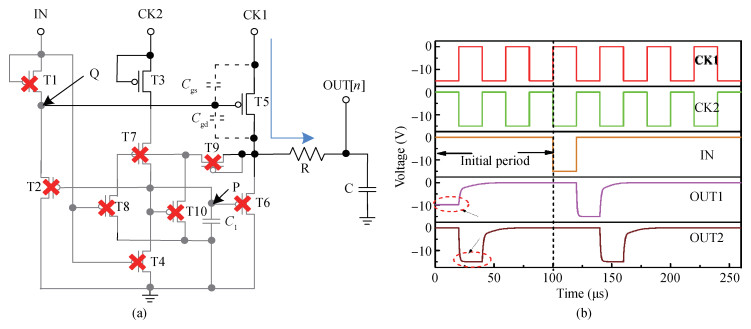
Fig. 1.
(Color online) The conventional gate driver with schematic of (a) single stage and (b) timing diagram.
SEMICONDUCTOR INTEGRATED CIRCUITS
Meng Chen, Jiefeng Lei, Shengxiang Huang, Congwei Liao and Lianwen Deng
Corresponding author: Liao Congwei, Email: 289114489@qq.com
Abstract: A p-type low-temperature poly-Si thin film transistors (LTPS TFTs) integrated gate driver using 2 non-overlapped clocks is proposed. This gate driver features charge-sharing structure to turn off buffer TFT and suppresses voltage feed-through effects. It is analyzed that the conventional gate driver suffers from waveform distortions due to voltage uncertainty of internal nodes for the initial period. The proposed charge-sharing structure also helps to suppress the unexpected pulses during the initialization phases. The proposed gate driver shows a simple circuit, as only 6 TFTs and 1 capacitor are used for single-stage, and the buffer TFT is used for both pulling-down and pulling-up of output electrode. Feasibility of the proposed gate driver is proven through detailed analyses. Investigations show that voltage bootrapping can be maintained once the bootrapping capacitance is larger than 0.8 pF, and pulse of gate driver outputs can be reduced to 5 μs. The proposed gate driver can still function properly with positive VTH shift within 0.4 V and negative VTH shift within-1.2 V and it is robust and promising for high-resolution display.
Keywords: LTPS TFT, charge-sharing, integrated gate driver
| [1] |
Kim S Y, Roy K. A low-cost low-noise amplifier in poly-Si TFT technology. J Display Technol, 2014, 10(12): 1110 doi: 10.1109/JDT.2014.2351617
|
| [2] |
Sazonov A, Striakhilev D, Lee C H, et al. Low-temperature materials and thin film transistor flexible electronics. Proc IEEE, 2005, 93(8): 1420 doi: 10.1109/JPROC.2005.851497
|
| [3] |
Stewart M, Howell R S, Pires L, et al. Poly silicon TFT technology for active matrix OLED displays. IEEE Trans Electron Devices, 2001, 48(5): 845 doi: 10.1109/16.918227
|
| [4] |
Zhang Y W, Chen W B. A new LTPS TFT AC pixel circuit for an AMOLED. J Semicond, 2013, 34(1): 015009 doi: 10.1088/1674-4926/34/1/015009
|
| [5] |
Ayres J R, Brotherton S D, Mcculloch D J, et al. Analysis of drain field and hot carrier stability of poly-Si thin film transistors. Jpn J Appl Phys, 1998, 37(4A): 1801 doi: 10.1143/JJAP.37.1801/pdf
|
| [6] |
Uraoka Y, Hatayama T, Fuyuki T, et al. Reliability of low temperature poly-silicon TFTs under inverter operation. IEEE Trans Electron Devices, 2001, 48(10): 2370 doi: 10.1109/16.954479
|
| [7] |
Meng Z G, Kwok H S, Wu C Y, et al. Fabrication of a 125 mm poly-Si TFT active-matrix driving color AMOLED. J Semicond, 2006, 27(8): 1514 http://en.cnki.com.cn/Article_en/CJFDTOTAL-BDTX200608036.htm
|
| [8] |
Schropp R E I, Stannowski B, Rath J K. New challenges in thin film transistor (TFT) research. J Non-Cryst Solids, 2002, 302(01): 1304 http://cat.inist.fr/?aModele=afficheN&cpsidt=14187909
|
| [9] |
Lin C L, Tu C D, Wu C E, et al. Low-power gate driver circuit for TFT-LCD application. IEEE Trans Electron Devices, 2012, 59(5): 1410 doi: 10.1109/TED.2012.2186966
|
| [10] |
Ha Y M. P-type technology for large size low temperature poly-Si TFT-LCDs. SID'00 Digest, 2000: 1116 doi: 10.1889/1.1832861/abstract;jsessionid=72683787C5EAE246D45FFE224B7C03AB.f03t04
|
| [11] |
Song E, Nam H. Shoot-through current reduction scheme for low power LTPS TFT programmable shift register. J Soc Inform Display, 2014, 22(1): 18 doi: 10.1002/jsid.219
|
| [12] |
Song E, Kang B, Han I, et al. Depletion mode oxide TFT shift register for variable frame rate AMOLED displays. IEEE Electron Device Lett, 2015, 36(3): 247 doi: 10.1109/LED.2015.2388471
|
| [13] |
Song S J, Kim B H, Jang J, et al. Low power low temperature poly-Si thin-film transistor shift register with DC-type output driver. Solid-State Electron, 2015, 111: 204 doi: 10.1016/j.sse.2015.06.010
|
| [14] |
Lin C L, Chen F H, Ciou W C, et al. Simplified gate driver circuit for high-resolution and narrow-bezel thin-film transistor liquid crystal display applications. IEEE Electron Device Lett, 2015, 36(8): 808 doi: 10.1109/LED.2015.2450231
|
| [15] |
Lin C L, Cheng M H, Tu C D, et al. 2-D-3-D switchable gate driver circuit for TFT-LCD applications. IEEE Trans Electron Devices, 2014, 61(6): 2098 doi: 10.1109/TED.2014.2319096
|
| [16] |
Lin C L, Cheng M H, Tu C D, et al. Low-power a-Si:H gate driver circuit with threshold-voltage-shift recovery and synchronously controlled pull-down scheme. IEEE Trans Electron Devices, 2015, 62(1): 136 doi: 10.1109/TED.2014.2372820
|
| [17] |
Song E, Nam H. Low power programmable shift register with depletion mode oxide TFTs for high resolution, and high frame rate AMFPDs. J Display Technol, 2014, 10(10): 834 https://www.osapublishing.org/jdt/abstract.cfm?uri=jdt-10-10-834
|
| [18] |
Jung S H, Kang S H, Song I H, et al. 2 clock shift register by employing p-type poly-Si TFTs for active matrix displays. ASID, 2002, 2002: 2 http://en.cnki.com.cn/Article_en/CJFDTOTAL-DZQJ200801020.htm
|
| [19] |
Chu L W, Liu P T, Ker M D. Design of integrated gate driver with threshold voltage drop cancellation in amorphous silicon technology for TFT-LCD application. J Display Technol, 2011, 7(12): 657 doi: 10.1109/JDT.2011.2162937
|
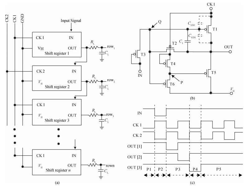
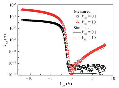
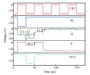
Table 1. Device parameters of LTPS TFT.

|
Table 2. Device parameters of the integrated gate driver.

|
| [1] |
Kim S Y, Roy K. A low-cost low-noise amplifier in poly-Si TFT technology. J Display Technol, 2014, 10(12): 1110 doi: 10.1109/JDT.2014.2351617
|
| [2] |
Sazonov A, Striakhilev D, Lee C H, et al. Low-temperature materials and thin film transistor flexible electronics. Proc IEEE, 2005, 93(8): 1420 doi: 10.1109/JPROC.2005.851497
|
| [3] |
Stewart M, Howell R S, Pires L, et al. Poly silicon TFT technology for active matrix OLED displays. IEEE Trans Electron Devices, 2001, 48(5): 845 doi: 10.1109/16.918227
|
| [4] |
Zhang Y W, Chen W B. A new LTPS TFT AC pixel circuit for an AMOLED. J Semicond, 2013, 34(1): 015009 doi: 10.1088/1674-4926/34/1/015009
|
| [5] |
Ayres J R, Brotherton S D, Mcculloch D J, et al. Analysis of drain field and hot carrier stability of poly-Si thin film transistors. Jpn J Appl Phys, 1998, 37(4A): 1801 doi: 10.1143/JJAP.37.1801/pdf
|
| [6] |
Uraoka Y, Hatayama T, Fuyuki T, et al. Reliability of low temperature poly-silicon TFTs under inverter operation. IEEE Trans Electron Devices, 2001, 48(10): 2370 doi: 10.1109/16.954479
|
| [7] |
Meng Z G, Kwok H S, Wu C Y, et al. Fabrication of a 125 mm poly-Si TFT active-matrix driving color AMOLED. J Semicond, 2006, 27(8): 1514 http://en.cnki.com.cn/Article_en/CJFDTOTAL-BDTX200608036.htm
|
| [8] |
Schropp R E I, Stannowski B, Rath J K. New challenges in thin film transistor (TFT) research. J Non-Cryst Solids, 2002, 302(01): 1304 http://cat.inist.fr/?aModele=afficheN&cpsidt=14187909
|
| [9] |
Lin C L, Tu C D, Wu C E, et al. Low-power gate driver circuit for TFT-LCD application. IEEE Trans Electron Devices, 2012, 59(5): 1410 doi: 10.1109/TED.2012.2186966
|
| [10] |
Ha Y M. P-type technology for large size low temperature poly-Si TFT-LCDs. SID'00 Digest, 2000: 1116 doi: 10.1889/1.1832861/abstract;jsessionid=72683787C5EAE246D45FFE224B7C03AB.f03t04
|
| [11] |
Song E, Nam H. Shoot-through current reduction scheme for low power LTPS TFT programmable shift register. J Soc Inform Display, 2014, 22(1): 18 doi: 10.1002/jsid.219
|
| [12] |
Song E, Kang B, Han I, et al. Depletion mode oxide TFT shift register for variable frame rate AMOLED displays. IEEE Electron Device Lett, 2015, 36(3): 247 doi: 10.1109/LED.2015.2388471
|
| [13] |
Song S J, Kim B H, Jang J, et al. Low power low temperature poly-Si thin-film transistor shift register with DC-type output driver. Solid-State Electron, 2015, 111: 204 doi: 10.1016/j.sse.2015.06.010
|
| [14] |
Lin C L, Chen F H, Ciou W C, et al. Simplified gate driver circuit for high-resolution and narrow-bezel thin-film transistor liquid crystal display applications. IEEE Electron Device Lett, 2015, 36(8): 808 doi: 10.1109/LED.2015.2450231
|
| [15] |
Lin C L, Cheng M H, Tu C D, et al. 2-D-3-D switchable gate driver circuit for TFT-LCD applications. IEEE Trans Electron Devices, 2014, 61(6): 2098 doi: 10.1109/TED.2014.2319096
|
| [16] |
Lin C L, Cheng M H, Tu C D, et al. Low-power a-Si:H gate driver circuit with threshold-voltage-shift recovery and synchronously controlled pull-down scheme. IEEE Trans Electron Devices, 2015, 62(1): 136 doi: 10.1109/TED.2014.2372820
|
| [17] |
Song E, Nam H. Low power programmable shift register with depletion mode oxide TFTs for high resolution, and high frame rate AMFPDs. J Display Technol, 2014, 10(10): 834 https://www.osapublishing.org/jdt/abstract.cfm?uri=jdt-10-10-834
|
| [18] |
Jung S H, Kang S H, Song I H, et al. 2 clock shift register by employing p-type poly-Si TFTs for active matrix displays. ASID, 2002, 2002: 2 http://en.cnki.com.cn/Article_en/CJFDTOTAL-DZQJ200801020.htm
|
| [19] |
Chu L W, Liu P T, Ker M D. Design of integrated gate driver with threshold voltage drop cancellation in amorphous silicon technology for TFT-LCD application. J Display Technol, 2011, 7(12): 657 doi: 10.1109/JDT.2011.2162937
|


Article views: 5041 Times PDF downloads: 116 Times Cited by: 0 Times
Received: 30 August 2016 Revised: 10 October 2016 Online: Published: 01 May 2017
| Citation: |
Meng Chen, Jiefeng Lei, Shengxiang Huang, Congwei Liao, Lianwen Deng. Poly-Si TFTs integrated gate driver circuit with charge-sharing structure[J]. Journal of Semiconductors, 2017, 38(5): 055001. doi: 10.1088/1674-4926/38/5/055001
****
M Chen, J F Lei, S X Huang, C W Liao, L W Deng. Poly-Si TFTs integrated gate driver circuit with charge-sharing structure[J]. J. Semicond., 2017, 38(5): 055001. doi: 10.1088/1674-4926/38/5/055001.

|
| [1] |
Kim S Y, Roy K. A low-cost low-noise amplifier in poly-Si TFT technology. J Display Technol, 2014, 10(12): 1110 doi: 10.1109/JDT.2014.2351617
|
| [2] |
Sazonov A, Striakhilev D, Lee C H, et al. Low-temperature materials and thin film transistor flexible electronics. Proc IEEE, 2005, 93(8): 1420 doi: 10.1109/JPROC.2005.851497
|
| [3] |
Stewart M, Howell R S, Pires L, et al. Poly silicon TFT technology for active matrix OLED displays. IEEE Trans Electron Devices, 2001, 48(5): 845 doi: 10.1109/16.918227
|
| [4] |
Zhang Y W, Chen W B. A new LTPS TFT AC pixel circuit for an AMOLED. J Semicond, 2013, 34(1): 015009 doi: 10.1088/1674-4926/34/1/015009
|
| [5] |
Ayres J R, Brotherton S D, Mcculloch D J, et al. Analysis of drain field and hot carrier stability of poly-Si thin film transistors. Jpn J Appl Phys, 1998, 37(4A): 1801 doi: 10.1143/JJAP.37.1801/pdf
|
| [6] |
Uraoka Y, Hatayama T, Fuyuki T, et al. Reliability of low temperature poly-silicon TFTs under inverter operation. IEEE Trans Electron Devices, 2001, 48(10): 2370 doi: 10.1109/16.954479
|
| [7] |
Meng Z G, Kwok H S, Wu C Y, et al. Fabrication of a 125 mm poly-Si TFT active-matrix driving color AMOLED. J Semicond, 2006, 27(8): 1514 http://en.cnki.com.cn/Article_en/CJFDTOTAL-BDTX200608036.htm
|
| [8] |
Schropp R E I, Stannowski B, Rath J K. New challenges in thin film transistor (TFT) research. J Non-Cryst Solids, 2002, 302(01): 1304 http://cat.inist.fr/?aModele=afficheN&cpsidt=14187909
|
| [9] |
Lin C L, Tu C D, Wu C E, et al. Low-power gate driver circuit for TFT-LCD application. IEEE Trans Electron Devices, 2012, 59(5): 1410 doi: 10.1109/TED.2012.2186966
|
| [10] |
Ha Y M. P-type technology for large size low temperature poly-Si TFT-LCDs. SID'00 Digest, 2000: 1116 doi: 10.1889/1.1832861/abstract;jsessionid=72683787C5EAE246D45FFE224B7C03AB.f03t04
|
| [11] |
Song E, Nam H. Shoot-through current reduction scheme for low power LTPS TFT programmable shift register. J Soc Inform Display, 2014, 22(1): 18 doi: 10.1002/jsid.219
|
| [12] |
Song E, Kang B, Han I, et al. Depletion mode oxide TFT shift register for variable frame rate AMOLED displays. IEEE Electron Device Lett, 2015, 36(3): 247 doi: 10.1109/LED.2015.2388471
|
| [13] |
Song S J, Kim B H, Jang J, et al. Low power low temperature poly-Si thin-film transistor shift register with DC-type output driver. Solid-State Electron, 2015, 111: 204 doi: 10.1016/j.sse.2015.06.010
|
| [14] |
Lin C L, Chen F H, Ciou W C, et al. Simplified gate driver circuit for high-resolution and narrow-bezel thin-film transistor liquid crystal display applications. IEEE Electron Device Lett, 2015, 36(8): 808 doi: 10.1109/LED.2015.2450231
|
| [15] |
Lin C L, Cheng M H, Tu C D, et al. 2-D-3-D switchable gate driver circuit for TFT-LCD applications. IEEE Trans Electron Devices, 2014, 61(6): 2098 doi: 10.1109/TED.2014.2319096
|
| [16] |
Lin C L, Cheng M H, Tu C D, et al. Low-power a-Si:H gate driver circuit with threshold-voltage-shift recovery and synchronously controlled pull-down scheme. IEEE Trans Electron Devices, 2015, 62(1): 136 doi: 10.1109/TED.2014.2372820
|
| [17] |
Song E, Nam H. Low power programmable shift register with depletion mode oxide TFTs for high resolution, and high frame rate AMFPDs. J Display Technol, 2014, 10(10): 834 https://www.osapublishing.org/jdt/abstract.cfm?uri=jdt-10-10-834
|
| [18] |
Jung S H, Kang S H, Song I H, et al. 2 clock shift register by employing p-type poly-Si TFTs for active matrix displays. ASID, 2002, 2002: 2 http://en.cnki.com.cn/Article_en/CJFDTOTAL-DZQJ200801020.htm
|
| [19] |
Chu L W, Liu P T, Ker M D. Design of integrated gate driver with threshold voltage drop cancellation in amorphous silicon technology for TFT-LCD application. J Display Technol, 2011, 7(12): 657 doi: 10.1109/JDT.2011.2162937
|

 WeChat ID
Journal of Semiconductors © 2017 All Rights Reserved 京ICP备05085259号-2

 DownLoad:

