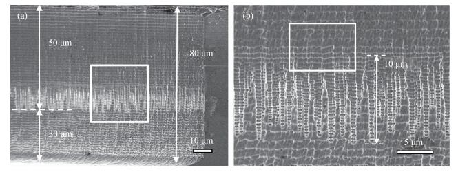
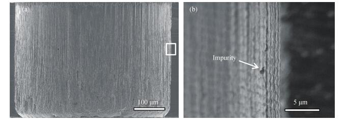
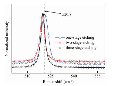
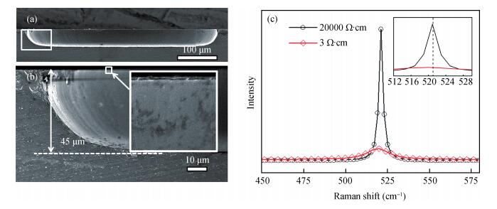
| [1] |
Li R, Jin C, Ong S C, et al. Embedded wafer level packaging for 77-GHz automotive radar front-end with through silicon via and its 3-D integration. IEEE Trans Compon, Packag Manufact Technol, 2013, 3: 1481 doi: 10.1109/TCPMT.2012.2236385 |
| [2] |
Lincelles J B, Marcelot O, Magnan P, et al. Enhanced nearinfrared response CMOS image sensors using high-resistivity substrate: photodiodes design impact on performances. IEEE Trans Electron Devices, 2016, 63: 120 doi: 10.1109/TED.2015.2477897 |
| [3] |
Chahat N, Tang A, Lee C, et al. Efficient CMOS systems with beam-lead interconnects for space instruments. IEEE Trans Terahertz Sci Technol, 2015, 5: 637 doi: 10.1109/TTHZ.2015.2446200 |
| [4] |
Ok S J, Kim C, Baldwin D F. High density, high aspect ratio through-wafer electrical interconnect vias for MEMS packaging. IEEE Trans Adv Packag, 2003, 26: 302 doi: 10.1109/TADVP.2003.818060 |
| [5] |
Fischer A C, Bleiker S J, Haraldsson T, et al. Very high aspect ratio through-silicon vias (TSVs) fabricated using automated magnetic assembly of nickel wires. J Micromechan Microeng, 2012, 22: 105001 doi: 10.1088/0960-1317/22/10/105001 |
| [6] |
|
| [7] |
Ren Z, McNie M E. Inductively coupled plasma etching of tapered via in silicon for MEMS integration. Microelectron Eng, 2015, 141: 261 doi: 10.1016/j.mee.2015.03.071 |
| [8] |
Jo S B, Lee M W, Lee S G, et al. Characterization of a modified Bosch-type process for silicon mold fabrication. J Vac Sci Technol A, 2005, 23: 905 doi: 10.1116/1.1943467 |
| [9] |
Li R, Lamy Y, Besling W F A, et al. Continuous deep reactive ion etching of tapered via holes for three-dimensional integration. J Micromechan Microeng, 2008, 18: 125023 doi: 10.1088/0960-1317/18/12/125023 |
| [10] |
Lee Y H, Chen M M. Silicon doping effects in reactive plasma etching. J Vac Sci Technol B, 1986, 4: 468 doi: 10.1116/1.583405 |
| [11] |
Bleiker S J, Fischer A C, Shah U, et al. High-aspect-ratio through silicon vias for high-frequency application fabricated by magnetic assembly of gold-coated nickel wires. IEEE Trans Compon, Packag Manufact Technol, 2015, 5: 21 doi: 10.1109/TCPMT.2014.2369236 |
| [12] |
Wu B Q, Kumar A, Pamarthy S. High aspect ratio silicon etch: a review. J Appl Phys, 2010, 108: 051101 doi: 10.1063/1.3474652 |
| [13] |
Bates R L, Thamban P L S, Goeckner M J, et al. Silicon etch using SF 6/C 4F 8/Ar gas mixtures. J Vac Sci Technol A, 2014, 32: 041302 doi: 10.1116/1.4880800 |
| [14] |
Li C T, Hsieh F C, Wang L. Performance improvement of p-type silicon solar cells with thin silicon films deposited by low pressure chemical vapor deposition method. Sol Energy, 2013, 88: 104 doi: 10.1016/j.solener.2012.12.001 |
| [15] |
Smit C, Van Swaaij R A C M M, Donker H, et al. Determining the material structure of microcrystalline silicon from Raman spectra. J Appl Phys, 2003, 94: 3582 doi: 10.1063/1.1596364 |
| [16] |
|
| [17] |
Pessoa R S, Maciel H S, Petraconi G, et al. Effect of gas residence time on the morphology of silicon surface etched in SF 6 plasmas. Appl Surf Sci, 2008, 255: 749 doi: 10.1016/j.apsusc.2008.07.057 |
| [18] |
Waits C M, Morgan B, Kastantin M, et al. Microfabrication of 3D silicon MEMS structures using gray-scale lithography and deep reactive ion etching. Sens Actuators A, 2005, 119: 245 doi: 10.1016/S0924-4247(04)00193-1 |
| [19] |
|
| [20] |
Lill T, Grimbergen M, Mui D. In situ measurement of aspect ratio dependent etch rates of polysilicon in an inductively coupled fluorine plasma. J Vac Sci Technol B, 2001, 19: 2123 doi: 10.1116/1.1415514 |
| [21] |
Chang C, Wang Y F, Kanamori Y, et al. Etching submicrometer trenches by using the Bosch process and its application to the fabrication of antireflection structures. J Micromechan Microeng, 2005, 15: 580 doi: 10.1088/0960-1317/15/3/020 |
| [22] |
Lee H C, Hong S P, Kang S K, et al. Residual stress on nanocrystalline silicon thin films deposited under energetic ion bombardment by using internal ICP-CVD. Thin Solid Films, 2009, 517: 4100 doi: 10.1016/j.tsf.2009.01.140 |


 DownLoad: