


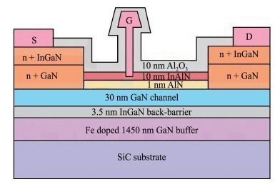
Fig. 1.
30 nm InAlN/AlN/GaN HEMT with InGaN back-barrier.
SEMICONDUCTOR DEVICES
P. Murugapandiyan1, , S. Ravimaran2 and J. William3
Corresponding author: P.Murugapandiyan, Email:murugavlsi@gmail.com
Abstract: The DC and RF performance of 30 nm gate length enhancement mode (E-mode) InAlN/AlN/GaN high electron mobility transistor (HEMT) on SiC substrate with heavily doped source and drain region have been investigated using the Synopsys TCAD tool. The proposed device has the features of a recessed T-gate structure, InGaN back barrier and Al2O3 passivated device surface. The proposed HEMT exhibits a maximum drain current density of 2.1 A/mm, transconductance gm of 1050 mS/mm, current gain cut-off frequency ft of 350 GHz and power gain cut-off frequency fmax of 340 GHz. At room temperature the measured carrier mobility (μ), sheet charge carrier density (ns) and breakdown voltage are 1580 cm2/(V·s), 1.9×1013 cm-2, and 10.7 V respectively. The superlatives of the proposed HEMTs are bewitching competitor or future sub-millimeter wave high power RF VLSI circuit applications.
Keywords: HEMT, back-barrier, recessed gate, cut-off frequency, regrown ohmic contact, short channel effects
| [1] |
Mishra U K, Shen L K, Kazior T E, et al. GaN-based RF power devices and amplifiers. Proc IEEE, 2008, 96:287 doi: 10.1109/JPROC.2007.911060
|
| [2] |
Arulkumaran S, Egawa T, Selvaraj L, et al. On the effects of gaterecess etching in current-collapse of different cap layers grown AlGaN/GaN high-electron-mobility transistors. Jpn J Appl Phys, 2006, 45:L220 doi: 10.1143/JJAP.45.L220
|
| [3] |
Drozdovski N V, Caverly R H. GaN-based high electronmobility transistors for microwave and RF control applications. IEEE Trans Microwave Theory Tech, 2002, 50:4 doi: 10.1109/22.981235
|
| [4] |
Shinohara K, Regan D C, Tang Y, et al. Scaling of GaN HEMTs and Schottky diodes for submillimeter-wave MMIC applications. IEEE Electron Device Lett, 2013, 60:2982 doi: 10.1109/TED.2013.2268160
|
| [5] |
Schwantuschke D, Brückner P, Quay R, et al. High-gain millimeter-wave AlGaN/GaN transistors. IEEE Trans Electron Devices, 2013, 60:3112 doi: 10.1109/TED.2013.2272180
|
| [6] |
Fitch R C, Walker D E, Green A J, et al. Implementation of highpower-density X-band AlGaN/GaN high electron mobility transistors in a millimeter-wave monolithic microwave integrated circuit process. IEEE Electron Device Lett, 2015, 36:1004 doi: 10.1109/LED.2015.2474265
|
| [7] |
Higashiwaki M, Mimura T, Matsui T. AlGaN/GaN heterostructure field-effect transistors on 4H-SiC substrates with currentgain cutoff frequency of 190 GHz. Appl Phys Exp, 2008, 1:021103 doi: 10.1143/APEX.1.021103
|
| [8] |
Zimmermann T, Deen D, Cao Y, et al. AlN/GaN insulated-gate HEMTs with 2.3 A/mm output current and 480 mS/mm transconductance. IEEE Electron Device Lett, 2008, 29:661 doi: 10.1109/LED.2008.923318
|
| [9] |
Bisi D, Chini A, Soci F, et al. Hot-electron degradation of AlGaN/GaN high-electron mobility transistors during RF operation:correlation with GaN buffer design. IEEE Electron Device Lett, 2015, 36:1011 doi: 10.1109/LED.2015.2474116
|
| [10] |
Chung J W, Hoke W E, Chumbes E M, et al. AlGaN/GaN HEMT with 300-GHz fmax. IEEE Electron Device Lett, 2010, 31:195 doi: 10.1109/LED.2009.2038935
|
| [11] |
Kuzmík J. Power electronics on InAlN/(In)GaN:prospect for a record performance. IEEE Electron Device Lett, 2001, 22:510 doi: 10.1109/55.962646
|
| [12] |
Marti D, Tirelli S, Teppati V, et al. 94-GHz large-signal operation of AlInN/GaN high-electron-mobility transistors on silicon with regrown ohmic contacts. IEEE Electron Device Lett, 2015, 36:17 doi: 10.1109/LED.2014.2367093
|
| [13] |
Kuzmík J, Kostopoulos A, Konstantinidis G, et al. InAlN/GaN HEMTs:a first insight into technological optimization. IEEE Trans Electron Devices, 2006, 53:422 doi: 10.1109/TED.2005.864379
|
| [14] |
Lugani L, Carlin J, Py M A, et al. Ultrathin InAlN/GaN heterostructures on sapphire for high on/off current ratio high electron mobility transistors. J Appl Phys, 2013, 113:214503 doi: 10.1063/1.4808260
|
| [15] |
Sun H F, Alt A R, Benedickter H, et al. 205-GHz (Al, In)N/GaN HEMTs. IEEE Electron Device Lett, 2010, 31:957 doi: 10.1109/LED.2010.2055826
|
| [16] |
Tirelli S, Marti D, Sun H F, et al. Fully passivated AlInN/GaN HEMTs with fT=fMAX of 205/220 GHz. IEEE Electron Device Lett, 2011, 32:1364 doi: 10.1109/LED.2011.2162087
|
| [17] |
Wang R H, Li G W, Laboutin O, et al. 210-GHz InAlN/GaN HEMTs with dielectric-free passivation. IEEE Electron Device Lett, 2011, 32:892 doi: 10.1109/LED.2011.2147753
|
| [18] |
Downey B P, Meyer D J, Katzer D J, et al. SiNx/InAlN/AlN/GaN MIS-HEMTs with 10.8 THz V Johnson figure of merit. IEEE Electron Device Lett, 2014, 35:527 doi: 10.1109/LED.2014.2313023
|
| [19] |
Lee D S, Gao X, Guo S P, et al. 300-GHz InAlN/GaN HEMTs with InGaN back barrier. IEEE Electron Device Lett, 2011, 32:1525 doi: 10.1109/LED.2011.2164613
|
| [20] |
Yue Y Z, Hu Z Y, Guo J, et al. InAlN/AlN/GaN HEMTs with regrown ohmic contacts and fT of 370 GHz. IEEE Electron Device Lett, 2012, 33:988 doi: 10.1109/LED.2012.2196751
|
| [21] |
Yue Y Z, Hu Z Y, Guo J, et al. Ultrascaled InAlN/GaN high electron mobility transistors with cutoff frequency of 400 GHz. Jpn J Appl Phys, 2013, 52:08JN14-1 https://www.researchgate.net/publication/260972645_Ultrascaled_InAlNGaN_High_Electron_Mobility_Transistors_with_Cutoff_Frequency_of_400_GHz
|
| [22] |
Lee H S, Piedra D, Sun M, et al. 3000-V 4.3-mΩ cm2 InAlN/GaN MOSHEMTs with AlGaN back barrier. IEEE Electron Device Lett, 2012, 33:982 doi: 10.1109/LED.2012.2196673
|
| [23] |
Chung J W, Saadat O I, Tirado J M, et al. Gate-recessed InAlN/GaN HEMTs on SiC substrate with Al2O3 passivation. IEEE Electron Device Lett, 2009, 30:904 doi: 10.1109/LED.2009.2026718
|
| [24] |
Wang R H, Saunier P, Xing X, et al. Gate-recessed enhancementmode InAlN/AlN/GaN HEMTs with 1.9-A/mm drain current density and 800-mS/mm transconductance. IEEE Electron Device Lett, 2010, 31:1383 doi: 10.1109/LED.2010.2072771
|
| [25] |
Kuzmik J, Ostermaier C, Pozzovivo G, et al. Proposal and performance analysis of normally off nCC GaN/InAlN/AlN/GaN HEMTs with 1-nm-thick InAlN barrier. IEEE Trans Electron Devices, 2010, 57:988 https://www.researchgate.net/publication/224157061_Proposal_and_performance_analysis_of_normally_off_n_GaNInAlNAlNGaN_HEMTs_with_1-nm-thick_InAlN_barrier
|
| [26] |
Crespo A, Bellot M M, Chabak K D, et al. High-power Kaband performance of AlInN/GaN HEMT with 9.8-nm-thin barrier. IEEE Electron Device Lett, 2010, 31:2 doi: 10.1109/LED.2009.2034875
|
| [27] |
Medjdoub F, Carlin J F, Gonschorek M, et al. Can InAlN/GaN be an alternative to high power/high temperature AlGaN/GaN devices. IEDM Tech Dig, 2006:673 https://www.researchgate.net/publication/224697680_Can_InAlNGaN_be_an_alternative_to_high_power_high_temperature_AlGaNGaN_devices
|
| [28] |
Palacios T, Chakraborty A, Heikman S, et al. AlGaN/GaN high electron mobility transistors with InGaN back-barriers. IEEE Electron Device Lett, 2006, 27:13 doi: 10.1109/LED.2005.860882
|
| [29] |
Chung J W, Saadat O I, TIirado J M, et al. Gate recessed InAlN/GaN HEMTs on SiC substrate with Al2O3 passivation. IEEE Electron Device Lett, 2009, 30:904 doi: 10.1109/LED.2009.2026718
|
| [30] |
Bouzid-Driad S, Maher H, Defrance N, et al. AlGaN/GaN HEMTs on silicon substrate with 206-GHz FMAX. IEEE Electron Device Lett, 2013, 34:36 doi: 10.1109/LED.2012.2224313
|
| [31] |
Khan M A, Kuznia J N, Bhattarai A R, et al. Metal semiconductor field effect transistor based on single crystal GaN. Appl Phys Lett, 1993, 62:1786 doi: 10.1063/1.109549
|
| [32] |
Khan M A, Bhattarai A, Kuznia J N, et al. High electron mobility transistor based on GaN/AlGaN heterojunction. Appl Phys Lett, 1993, 63:1214 doi: 10.1063/1.109775
|
| [33] |
Lee D S, Chung J W, Wang H, et al. 245 GHz InAlN/GaN HEMTs with oxygen plasma treatment. IEEE Electron Device Lett, 2011, 32:755 doi: 10.1109/LED.2011.2132751
|
| [34] |
Chung J W, Hoke W E, Chumbes E M. AlGaN/GaN HEMT with 300-GHz fmax. IEEE Electron Device Lett, 2009, 31:195
|
| [35] |
Song B, Sensale-Rodriguez B, Wang R H, et al. Effect of fringing capacitances on the RF performance of GaN HEMTs with T-gates. IEEE Electron Device Lett, 2014, 61:747 doi: 10.1109/TED.2014.2299810
|
| [36] |
Cico K, Gregusova D, Kuzmik J, et al. Influence of processing and annealing steps on electrical properties of InAlN/GaN high electron mobility transistor with Al2O3 gate insulation and passivation. Solid State Electron, 2012, 67:74 doi: 10.1016/j.sse.2011.09.002
|
| [37] |
Meyer D J, Bass R, Katzer E S, et al. Self aligned ALD AlOx Tgate insulator for gate leakage current suppression in SiNx passivated AlGaN/GaN HEMTs. Solid State Electron, 2010, 54:1098 doi: 10.1016/j.sse.2010.05.024
|
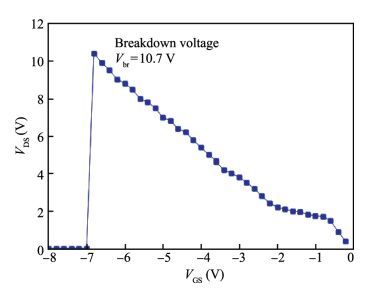
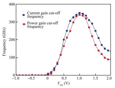
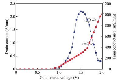
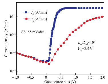
Table 1.
 |
| [1] |
Mishra U K, Shen L K, Kazior T E, et al. GaN-based RF power devices and amplifiers. Proc IEEE, 2008, 96:287 doi: 10.1109/JPROC.2007.911060
|
| [2] |
Arulkumaran S, Egawa T, Selvaraj L, et al. On the effects of gaterecess etching in current-collapse of different cap layers grown AlGaN/GaN high-electron-mobility transistors. Jpn J Appl Phys, 2006, 45:L220 doi: 10.1143/JJAP.45.L220
|
| [3] |
Drozdovski N V, Caverly R H. GaN-based high electronmobility transistors for microwave and RF control applications. IEEE Trans Microwave Theory Tech, 2002, 50:4 doi: 10.1109/22.981235
|
| [4] |
Shinohara K, Regan D C, Tang Y, et al. Scaling of GaN HEMTs and Schottky diodes for submillimeter-wave MMIC applications. IEEE Electron Device Lett, 2013, 60:2982 doi: 10.1109/TED.2013.2268160
|
| [5] |
Schwantuschke D, Brückner P, Quay R, et al. High-gain millimeter-wave AlGaN/GaN transistors. IEEE Trans Electron Devices, 2013, 60:3112 doi: 10.1109/TED.2013.2272180
|
| [6] |
Fitch R C, Walker D E, Green A J, et al. Implementation of highpower-density X-band AlGaN/GaN high electron mobility transistors in a millimeter-wave monolithic microwave integrated circuit process. IEEE Electron Device Lett, 2015, 36:1004 doi: 10.1109/LED.2015.2474265
|
| [7] |
Higashiwaki M, Mimura T, Matsui T. AlGaN/GaN heterostructure field-effect transistors on 4H-SiC substrates with currentgain cutoff frequency of 190 GHz. Appl Phys Exp, 2008, 1:021103 doi: 10.1143/APEX.1.021103
|
| [8] |
Zimmermann T, Deen D, Cao Y, et al. AlN/GaN insulated-gate HEMTs with 2.3 A/mm output current and 480 mS/mm transconductance. IEEE Electron Device Lett, 2008, 29:661 doi: 10.1109/LED.2008.923318
|
| [9] |
Bisi D, Chini A, Soci F, et al. Hot-electron degradation of AlGaN/GaN high-electron mobility transistors during RF operation:correlation with GaN buffer design. IEEE Electron Device Lett, 2015, 36:1011 doi: 10.1109/LED.2015.2474116
|
| [10] |
Chung J W, Hoke W E, Chumbes E M, et al. AlGaN/GaN HEMT with 300-GHz fmax. IEEE Electron Device Lett, 2010, 31:195 doi: 10.1109/LED.2009.2038935
|
| [11] |
Kuzmík J. Power electronics on InAlN/(In)GaN:prospect for a record performance. IEEE Electron Device Lett, 2001, 22:510 doi: 10.1109/55.962646
|
| [12] |
Marti D, Tirelli S, Teppati V, et al. 94-GHz large-signal operation of AlInN/GaN high-electron-mobility transistors on silicon with regrown ohmic contacts. IEEE Electron Device Lett, 2015, 36:17 doi: 10.1109/LED.2014.2367093
|
| [13] |
Kuzmík J, Kostopoulos A, Konstantinidis G, et al. InAlN/GaN HEMTs:a first insight into technological optimization. IEEE Trans Electron Devices, 2006, 53:422 doi: 10.1109/TED.2005.864379
|
| [14] |
Lugani L, Carlin J, Py M A, et al. Ultrathin InAlN/GaN heterostructures on sapphire for high on/off current ratio high electron mobility transistors. J Appl Phys, 2013, 113:214503 doi: 10.1063/1.4808260
|
| [15] |
Sun H F, Alt A R, Benedickter H, et al. 205-GHz (Al, In)N/GaN HEMTs. IEEE Electron Device Lett, 2010, 31:957 doi: 10.1109/LED.2010.2055826
|
| [16] |
Tirelli S, Marti D, Sun H F, et al. Fully passivated AlInN/GaN HEMTs with fT=fMAX of 205/220 GHz. IEEE Electron Device Lett, 2011, 32:1364 doi: 10.1109/LED.2011.2162087
|
| [17] |
Wang R H, Li G W, Laboutin O, et al. 210-GHz InAlN/GaN HEMTs with dielectric-free passivation. IEEE Electron Device Lett, 2011, 32:892 doi: 10.1109/LED.2011.2147753
|
| [18] |
Downey B P, Meyer D J, Katzer D J, et al. SiNx/InAlN/AlN/GaN MIS-HEMTs with 10.8 THz V Johnson figure of merit. IEEE Electron Device Lett, 2014, 35:527 doi: 10.1109/LED.2014.2313023
|
| [19] |
Lee D S, Gao X, Guo S P, et al. 300-GHz InAlN/GaN HEMTs with InGaN back barrier. IEEE Electron Device Lett, 2011, 32:1525 doi: 10.1109/LED.2011.2164613
|
| [20] |
Yue Y Z, Hu Z Y, Guo J, et al. InAlN/AlN/GaN HEMTs with regrown ohmic contacts and fT of 370 GHz. IEEE Electron Device Lett, 2012, 33:988 doi: 10.1109/LED.2012.2196751
|
| [21] |
Yue Y Z, Hu Z Y, Guo J, et al. Ultrascaled InAlN/GaN high electron mobility transistors with cutoff frequency of 400 GHz. Jpn J Appl Phys, 2013, 52:08JN14-1 https://www.researchgate.net/publication/260972645_Ultrascaled_InAlNGaN_High_Electron_Mobility_Transistors_with_Cutoff_Frequency_of_400_GHz
|
| [22] |
Lee H S, Piedra D, Sun M, et al. 3000-V 4.3-mΩ cm2 InAlN/GaN MOSHEMTs with AlGaN back barrier. IEEE Electron Device Lett, 2012, 33:982 doi: 10.1109/LED.2012.2196673
|
| [23] |
Chung J W, Saadat O I, Tirado J M, et al. Gate-recessed InAlN/GaN HEMTs on SiC substrate with Al2O3 passivation. IEEE Electron Device Lett, 2009, 30:904 doi: 10.1109/LED.2009.2026718
|
| [24] |
Wang R H, Saunier P, Xing X, et al. Gate-recessed enhancementmode InAlN/AlN/GaN HEMTs with 1.9-A/mm drain current density and 800-mS/mm transconductance. IEEE Electron Device Lett, 2010, 31:1383 doi: 10.1109/LED.2010.2072771
|
| [25] |
Kuzmik J, Ostermaier C, Pozzovivo G, et al. Proposal and performance analysis of normally off nCC GaN/InAlN/AlN/GaN HEMTs with 1-nm-thick InAlN barrier. IEEE Trans Electron Devices, 2010, 57:988 https://www.researchgate.net/publication/224157061_Proposal_and_performance_analysis_of_normally_off_n_GaNInAlNAlNGaN_HEMTs_with_1-nm-thick_InAlN_barrier
|
| [26] |
Crespo A, Bellot M M, Chabak K D, et al. High-power Kaband performance of AlInN/GaN HEMT with 9.8-nm-thin barrier. IEEE Electron Device Lett, 2010, 31:2 doi: 10.1109/LED.2009.2034875
|
| [27] |
Medjdoub F, Carlin J F, Gonschorek M, et al. Can InAlN/GaN be an alternative to high power/high temperature AlGaN/GaN devices. IEDM Tech Dig, 2006:673 https://www.researchgate.net/publication/224697680_Can_InAlNGaN_be_an_alternative_to_high_power_high_temperature_AlGaNGaN_devices
|
| [28] |
Palacios T, Chakraborty A, Heikman S, et al. AlGaN/GaN high electron mobility transistors with InGaN back-barriers. IEEE Electron Device Lett, 2006, 27:13 doi: 10.1109/LED.2005.860882
|
| [29] |
Chung J W, Saadat O I, TIirado J M, et al. Gate recessed InAlN/GaN HEMTs on SiC substrate with Al2O3 passivation. IEEE Electron Device Lett, 2009, 30:904 doi: 10.1109/LED.2009.2026718
|
| [30] |
Bouzid-Driad S, Maher H, Defrance N, et al. AlGaN/GaN HEMTs on silicon substrate with 206-GHz FMAX. IEEE Electron Device Lett, 2013, 34:36 doi: 10.1109/LED.2012.2224313
|
| [31] |
Khan M A, Kuznia J N, Bhattarai A R, et al. Metal semiconductor field effect transistor based on single crystal GaN. Appl Phys Lett, 1993, 62:1786 doi: 10.1063/1.109549
|
| [32] |
Khan M A, Bhattarai A, Kuznia J N, et al. High electron mobility transistor based on GaN/AlGaN heterojunction. Appl Phys Lett, 1993, 63:1214 doi: 10.1063/1.109775
|
| [33] |
Lee D S, Chung J W, Wang H, et al. 245 GHz InAlN/GaN HEMTs with oxygen plasma treatment. IEEE Electron Device Lett, 2011, 32:755 doi: 10.1109/LED.2011.2132751
|
| [34] |
Chung J W, Hoke W E, Chumbes E M. AlGaN/GaN HEMT with 300-GHz fmax. IEEE Electron Device Lett, 2009, 31:195
|
| [35] |
Song B, Sensale-Rodriguez B, Wang R H, et al. Effect of fringing capacitances on the RF performance of GaN HEMTs with T-gates. IEEE Electron Device Lett, 2014, 61:747 doi: 10.1109/TED.2014.2299810
|
| [36] |
Cico K, Gregusova D, Kuzmik J, et al. Influence of processing and annealing steps on electrical properties of InAlN/GaN high electron mobility transistor with Al2O3 gate insulation and passivation. Solid State Electron, 2012, 67:74 doi: 10.1016/j.sse.2011.09.002
|
| [37] |
Meyer D J, Bass R, Katzer E S, et al. Self aligned ALD AlOx Tgate insulator for gate leakage current suppression in SiNx passivated AlGaN/GaN HEMTs. Solid State Electron, 2010, 54:1098 doi: 10.1016/j.sse.2010.05.024
|


Article views: 3693 Times PDF downloads: 71 Times Cited by: 0 Times
Received: 07 September 2016 Revised: 07 February 2017 Online: Published: 01 August 2017
| Citation: |
P. Murugapandiyan, S. Ravimaran, J. William. 30 nm T-gate enhancement-mode InAlN/AlN/GaN HEMT on SiC substrates for future high power RF applications[J]. Journal of Semiconductors, 2017, 38(8): 084001. doi: 10.1088/1674-4926/38/8/084001
****
P. Murugapandiyan, S. Ravimaran, J. William. 30 nm T-gate enhancement-mode InAlN/AlN/GaN HEMT on SiC substrates for future high power RF applications[J]. J. Semicond., 2017, 38(8): 084001. doi: 10.1088/1674-4926/38/8/084001.

|
| [1] |
Mishra U K, Shen L K, Kazior T E, et al. GaN-based RF power devices and amplifiers. Proc IEEE, 2008, 96:287 doi: 10.1109/JPROC.2007.911060
|
| [2] |
Arulkumaran S, Egawa T, Selvaraj L, et al. On the effects of gaterecess etching in current-collapse of different cap layers grown AlGaN/GaN high-electron-mobility transistors. Jpn J Appl Phys, 2006, 45:L220 doi: 10.1143/JJAP.45.L220
|
| [3] |
Drozdovski N V, Caverly R H. GaN-based high electronmobility transistors for microwave and RF control applications. IEEE Trans Microwave Theory Tech, 2002, 50:4 doi: 10.1109/22.981235
|
| [4] |
Shinohara K, Regan D C, Tang Y, et al. Scaling of GaN HEMTs and Schottky diodes for submillimeter-wave MMIC applications. IEEE Electron Device Lett, 2013, 60:2982 doi: 10.1109/TED.2013.2268160
|
| [5] |
Schwantuschke D, Brückner P, Quay R, et al. High-gain millimeter-wave AlGaN/GaN transistors. IEEE Trans Electron Devices, 2013, 60:3112 doi: 10.1109/TED.2013.2272180
|
| [6] |
Fitch R C, Walker D E, Green A J, et al. Implementation of highpower-density X-band AlGaN/GaN high electron mobility transistors in a millimeter-wave monolithic microwave integrated circuit process. IEEE Electron Device Lett, 2015, 36:1004 doi: 10.1109/LED.2015.2474265
|
| [7] |
Higashiwaki M, Mimura T, Matsui T. AlGaN/GaN heterostructure field-effect transistors on 4H-SiC substrates with currentgain cutoff frequency of 190 GHz. Appl Phys Exp, 2008, 1:021103 doi: 10.1143/APEX.1.021103
|
| [8] |
Zimmermann T, Deen D, Cao Y, et al. AlN/GaN insulated-gate HEMTs with 2.3 A/mm output current and 480 mS/mm transconductance. IEEE Electron Device Lett, 2008, 29:661 doi: 10.1109/LED.2008.923318
|
| [9] |
Bisi D, Chini A, Soci F, et al. Hot-electron degradation of AlGaN/GaN high-electron mobility transistors during RF operation:correlation with GaN buffer design. IEEE Electron Device Lett, 2015, 36:1011 doi: 10.1109/LED.2015.2474116
|
| [10] |
Chung J W, Hoke W E, Chumbes E M, et al. AlGaN/GaN HEMT with 300-GHz fmax. IEEE Electron Device Lett, 2010, 31:195 doi: 10.1109/LED.2009.2038935
|
| [11] |
Kuzmík J. Power electronics on InAlN/(In)GaN:prospect for a record performance. IEEE Electron Device Lett, 2001, 22:510 doi: 10.1109/55.962646
|
| [12] |
Marti D, Tirelli S, Teppati V, et al. 94-GHz large-signal operation of AlInN/GaN high-electron-mobility transistors on silicon with regrown ohmic contacts. IEEE Electron Device Lett, 2015, 36:17 doi: 10.1109/LED.2014.2367093
|
| [13] |
Kuzmík J, Kostopoulos A, Konstantinidis G, et al. InAlN/GaN HEMTs:a first insight into technological optimization. IEEE Trans Electron Devices, 2006, 53:422 doi: 10.1109/TED.2005.864379
|
| [14] |
Lugani L, Carlin J, Py M A, et al. Ultrathin InAlN/GaN heterostructures on sapphire for high on/off current ratio high electron mobility transistors. J Appl Phys, 2013, 113:214503 doi: 10.1063/1.4808260
|
| [15] |
Sun H F, Alt A R, Benedickter H, et al. 205-GHz (Al, In)N/GaN HEMTs. IEEE Electron Device Lett, 2010, 31:957 doi: 10.1109/LED.2010.2055826
|
| [16] |
Tirelli S, Marti D, Sun H F, et al. Fully passivated AlInN/GaN HEMTs with fT=fMAX of 205/220 GHz. IEEE Electron Device Lett, 2011, 32:1364 doi: 10.1109/LED.2011.2162087
|
| [17] |
Wang R H, Li G W, Laboutin O, et al. 210-GHz InAlN/GaN HEMTs with dielectric-free passivation. IEEE Electron Device Lett, 2011, 32:892 doi: 10.1109/LED.2011.2147753
|
| [18] |
Downey B P, Meyer D J, Katzer D J, et al. SiNx/InAlN/AlN/GaN MIS-HEMTs with 10.8 THz V Johnson figure of merit. IEEE Electron Device Lett, 2014, 35:527 doi: 10.1109/LED.2014.2313023
|
| [19] |
Lee D S, Gao X, Guo S P, et al. 300-GHz InAlN/GaN HEMTs with InGaN back barrier. IEEE Electron Device Lett, 2011, 32:1525 doi: 10.1109/LED.2011.2164613
|
| [20] |
Yue Y Z, Hu Z Y, Guo J, et al. InAlN/AlN/GaN HEMTs with regrown ohmic contacts and fT of 370 GHz. IEEE Electron Device Lett, 2012, 33:988 doi: 10.1109/LED.2012.2196751
|
| [21] |
Yue Y Z, Hu Z Y, Guo J, et al. Ultrascaled InAlN/GaN high electron mobility transistors with cutoff frequency of 400 GHz. Jpn J Appl Phys, 2013, 52:08JN14-1 https://www.researchgate.net/publication/260972645_Ultrascaled_InAlNGaN_High_Electron_Mobility_Transistors_with_Cutoff_Frequency_of_400_GHz
|
| [22] |
Lee H S, Piedra D, Sun M, et al. 3000-V 4.3-mΩ cm2 InAlN/GaN MOSHEMTs with AlGaN back barrier. IEEE Electron Device Lett, 2012, 33:982 doi: 10.1109/LED.2012.2196673
|
| [23] |
Chung J W, Saadat O I, Tirado J M, et al. Gate-recessed InAlN/GaN HEMTs on SiC substrate with Al2O3 passivation. IEEE Electron Device Lett, 2009, 30:904 doi: 10.1109/LED.2009.2026718
|
| [24] |
Wang R H, Saunier P, Xing X, et al. Gate-recessed enhancementmode InAlN/AlN/GaN HEMTs with 1.9-A/mm drain current density and 800-mS/mm transconductance. IEEE Electron Device Lett, 2010, 31:1383 doi: 10.1109/LED.2010.2072771
|
| [25] |
Kuzmik J, Ostermaier C, Pozzovivo G, et al. Proposal and performance analysis of normally off nCC GaN/InAlN/AlN/GaN HEMTs with 1-nm-thick InAlN barrier. IEEE Trans Electron Devices, 2010, 57:988 https://www.researchgate.net/publication/224157061_Proposal_and_performance_analysis_of_normally_off_n_GaNInAlNAlNGaN_HEMTs_with_1-nm-thick_InAlN_barrier
|
| [26] |
Crespo A, Bellot M M, Chabak K D, et al. High-power Kaband performance of AlInN/GaN HEMT with 9.8-nm-thin barrier. IEEE Electron Device Lett, 2010, 31:2 doi: 10.1109/LED.2009.2034875
|
| [27] |
Medjdoub F, Carlin J F, Gonschorek M, et al. Can InAlN/GaN be an alternative to high power/high temperature AlGaN/GaN devices. IEDM Tech Dig, 2006:673 https://www.researchgate.net/publication/224697680_Can_InAlNGaN_be_an_alternative_to_high_power_high_temperature_AlGaNGaN_devices
|
| [28] |
Palacios T, Chakraborty A, Heikman S, et al. AlGaN/GaN high electron mobility transistors with InGaN back-barriers. IEEE Electron Device Lett, 2006, 27:13 doi: 10.1109/LED.2005.860882
|
| [29] |
Chung J W, Saadat O I, TIirado J M, et al. Gate recessed InAlN/GaN HEMTs on SiC substrate with Al2O3 passivation. IEEE Electron Device Lett, 2009, 30:904 doi: 10.1109/LED.2009.2026718
|
| [30] |
Bouzid-Driad S, Maher H, Defrance N, et al. AlGaN/GaN HEMTs on silicon substrate with 206-GHz FMAX. IEEE Electron Device Lett, 2013, 34:36 doi: 10.1109/LED.2012.2224313
|
| [31] |
Khan M A, Kuznia J N, Bhattarai A R, et al. Metal semiconductor field effect transistor based on single crystal GaN. Appl Phys Lett, 1993, 62:1786 doi: 10.1063/1.109549
|
| [32] |
Khan M A, Bhattarai A, Kuznia J N, et al. High electron mobility transistor based on GaN/AlGaN heterojunction. Appl Phys Lett, 1993, 63:1214 doi: 10.1063/1.109775
|
| [33] |
Lee D S, Chung J W, Wang H, et al. 245 GHz InAlN/GaN HEMTs with oxygen plasma treatment. IEEE Electron Device Lett, 2011, 32:755 doi: 10.1109/LED.2011.2132751
|
| [34] |
Chung J W, Hoke W E, Chumbes E M. AlGaN/GaN HEMT with 300-GHz fmax. IEEE Electron Device Lett, 2009, 31:195
|
| [35] |
Song B, Sensale-Rodriguez B, Wang R H, et al. Effect of fringing capacitances on the RF performance of GaN HEMTs with T-gates. IEEE Electron Device Lett, 2014, 61:747 doi: 10.1109/TED.2014.2299810
|
| [36] |
Cico K, Gregusova D, Kuzmik J, et al. Influence of processing and annealing steps on electrical properties of InAlN/GaN high electron mobility transistor with Al2O3 gate insulation and passivation. Solid State Electron, 2012, 67:74 doi: 10.1016/j.sse.2011.09.002
|
| [37] |
Meyer D J, Bass R, Katzer E S, et al. Self aligned ALD AlOx Tgate insulator for gate leakage current suppression in SiNx passivated AlGaN/GaN HEMTs. Solid State Electron, 2010, 54:1098 doi: 10.1016/j.sse.2010.05.024
|

 WeChat ID
Journal of Semiconductors © 2017 All Rights Reserved 京ICP备05085259号-2

 DownLoad:

