


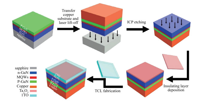
Fig. 1.
(Color online) Fabrication process of EIS structure based on the LED epilayers.
SEMICONDUCTOR DEVICES
Chenglin Qi, Yang Huang, Teng Zhan, Qinjin Wang, Xiaoyan Yi and Zhiqiang Liu
Corresponding author: Chenglin Qi, Email:qichenglin@semi.ac.cn
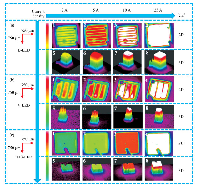
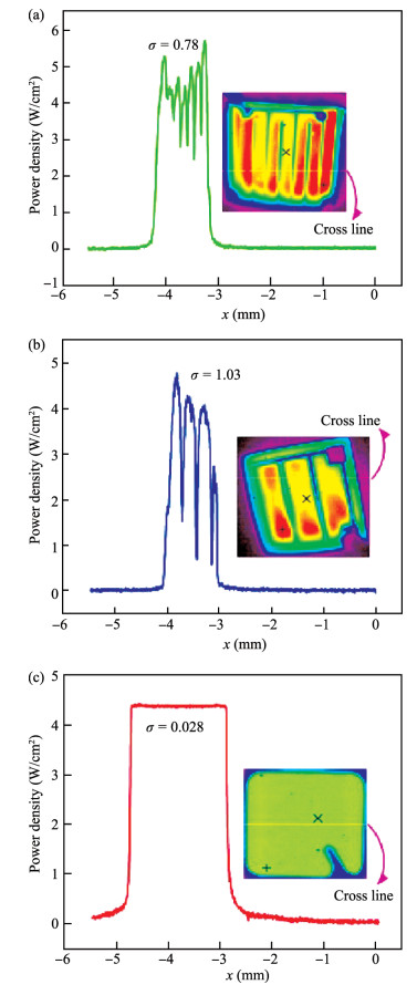
Abstract: GaN-based vertical light-emitting-diodes (V-LEDs) with an improved current injection pattern were fabricated and a novel current injection pattern of LEDs which consists of electrode-insulator-semiconductor (EIS) structure was proposed. The EIS structure was achieved by an insulator layer (20-nm Ta2O5) deposited between the p-GaN and the ITO layer. This kind of EIS structure works through a defect-assisted tunneling mechanism to realize current injection and obtains a uniform current distribution on the chip surface, thus greatly improving the current spreading ability of LEDs. The appearance of this novel current injection pattern of V-LEDs will subvert the impression of the conventional LEDs structure, including simplifying the chip manufacture technology and reducing the chip cost. Under a current density of 2, 5, 10, and 25 A/cm2, the luminous uniformity was better than conventional structure LEDs. The standard deviation of power density distribution in light distribution was 0.028, which was much smaller than that of conventional structure LEDs and illustrated a huge advantage on the current spreading ability of EIS-LEDs.
Keywords: electrode-insulator-semiconductor (EIS), light emitting diodes (LEDs), tunneling mechanism, luminous uniformity, current spreading
| [1] |
Singh S, Nandini A D S, Pal S, et al. Enhancement of light extraction efficiency of vertical LED with patterned graphene as current spreading layer. Superlattices Microstruct, 2016, 89:89 doi: 10.1016/j.spmi.2015.11.007
|
| [2] |
Cho J, Schubert E F, Kim J F. Efficiency droop in light-emitting diodes:challenges and countermeasures. Laser Photonics Rev, 2013, 7(3):408 doi: 10.1002/lpor.201200025
|
| [3] |
Verzellesi G, Saguatti D, Meneghini M, et al. Efficiency droop in InGaN/GaN blue light-emitting diodes:physical mechanisms and remedies. J Appl Phys, 2013, 114(7):14 doi: 10.1063/1.4816434
|
| [4] |
Zhang Y Y, Zheng H Y, Guo E Q, et al. Effects of light extraction efficiency to the efficiency droop of InGaN-based light-emitting diodes. J Appl Phys, 2013, 113(1):6 doi: 10.1063/1.4772669
|
| [5] |
Zhan T, Zhang Y, Ma J, et al. Characteristics of GaN-based highvoltage LEDs compared to traditional high power LEDs. IEEE Photonics Technol Lett, 2013, 25(9):844 doi: 10.1109/LPT.2013.2251878
|
| [6] |
Tajima J, Ono H, Ito T, et al. Fabrication and characteristics of high-power multijunction LEDs using GaN-on-Si technologies. Phys Status Solidi A, 2016, 213(5):1177 doi: 10.1002/pssa.v213.5
|
| [7] |
Kang D, Jung M, Choi E, et al. Comparison of the performance of lateral and vertical InGaN/GaN-based light-emitting diodes with GaN and AlN nucleation layers. ECS J Solid State Sci Technol, 2016, 5(2):Q1 doi: 10.1149/2.0011602jss
|
| [8] |
Malyutenko V K, Podoltsev A D, Malyutenko O Y. Current crowding impact at spatially and temporarily resolved thermal characters of large-area AlGaInP light emitting diodes operating in dimming/flashing modes. J Appl Phys, 2015, 118(15):153105 doi: 10.1063/1.4933390
|
| [9] |
Tian T, Zhan T, Guo J, et al. Transparent graphene interconnects for monolithic integration of GaN-based LEDs. Appl Phys Express, 2015, 8(4):042102 doi: 10.7567/APEX.8.042102
|
| [10] |
Kim S J, Kim H D, Kim K H, et al. Fabrication of wide-bandgap transparent electrodes by using conductive filaments:performance breakthrough in vertical-type GaN LED. Sci Rep, 2014, 4:5827 http://www.nature.com/srep/2014/140725/srep05827/full/srep05827.html?WT.ec_id=SREP-639-20140729
|
| [11] |
Tsai M L, Liao J H, Yeh J H, et al. High-voltage thin-film GaN LEDs fabricated on ceramic substrates:the alleviated droop effect at 670 W/cm2. Opt Express, 2013, 21(22):27102 doi: 10.1364/OE.21.027102
|
| [12] |
Cai Y, Zou X, Chong W C, et al. Optimization of electrode structure for flip-chip HVLED via two-level metallization. Physica Status Solidi A, 2016, 213(5):1199 doi: 10.1002/pssa.v213.5
|
| [13] |
Zhu W J, Ma T P, Tamagawa T, et al. Current transport in metal/hafnium oxide/silicon structure. IEEE Electron Device Lett, 2002, 23(2):97 doi: 10.1109/55.981318
|
| [14] |
Ning T H, Osburn C M, Yu H N. Hot-electron emission from silicon into silicon dioxide. Solid-State Electron, 1978, 21(1):273 doi: 10.1016/0038-1101(78)90148-X
|
| [15] |
Oh M, Jeong S, Gil Y, et al. Highly reflective Ti/Ag/Pt contacts to p-GaN for high-efficiency GaN-based light-emitting diodes. Jpn J Appl Phys, 2015, 54(2):5 doi: 10.7567/JJAP.54.02BB01
|
| [16] |
Tian T, Wang L C, Guo E Q, et al. Optimized subsequentannealing-free Ni/Ag based metallization contact to p-type GaN for vertical light emitting diodes with high yield and extremely low operating voltage (2.75 V@350 mA, > 95%). J Phys D, 2014, 47(11):7 https://www.researchgate.net/publication/260420312_Optimized_subsequent-annealing-free_NiAg_based_metallization_contact_to_p-type_GaN_for_vertical_light_emitting_diodes_with_high_yield_and_extremely_low_operating_voltage_275_V350_mA_95
|
| [17] |
Chen J L, Brewer W D. Ohmic contacts on p-GaN. Adv Electron Mater, 2015, 1(8):7 http://www.sciencedirect.com/science/article/pii/S1369800100001773
|
| [18] |
Cha Y J, Oh S K, Kwak J S. Low-damage sputtered silver ohmic contacts to p-GaN with thermal stability. Mater Lett, 2015, 158:363 doi: 10.1016/j.matlet.2015.05.169
|
| [19] |
Jung S, Song K R, Lee S N, et al. Wet chemical etching of semipolar GaN planes to obtain brighter and cost-competitive light emitters. Adv Mater, 2013, 25(32):4470 doi: 10.1002/adma.v25.32
|


Article views: 4524 Times PDF downloads: 67 Times Cited by: 0 Times
Received: 09 February 2017 Revised: 01 March 2017 Online: Published: 01 August 2017
| Citation: |
Chenglin Qi, Yang Huang, Teng Zhan, Qinjin Wang, Xiaoyan Yi, Zhiqiang Liu. Fabrication and characteristics of excellent current spreading GaN-based LED by using transparent electrode-insulator-semiconductor structure[J]. Journal of Semiconductors, 2017, 38(8): 084005. doi: 10.1088/1674-4926/38/8/084005
****
C L Qi, Y Huang, T Zhan, Q J Wang, X Y Yi, Z Q Liu. Fabrication and characteristics of excellent current spreading GaN-based LED by using transparent electrode-insulator-semiconductor structure[J]. J. Semicond., 2017, 38(8): 084005. doi: 10.1088/1674-4926/38/8/084005.

|
| [1] |
Singh S, Nandini A D S, Pal S, et al. Enhancement of light extraction efficiency of vertical LED with patterned graphene as current spreading layer. Superlattices Microstruct, 2016, 89:89 doi: 10.1016/j.spmi.2015.11.007
|
| [2] |
Cho J, Schubert E F, Kim J F. Efficiency droop in light-emitting diodes:challenges and countermeasures. Laser Photonics Rev, 2013, 7(3):408 doi: 10.1002/lpor.201200025
|
| [3] |
Verzellesi G, Saguatti D, Meneghini M, et al. Efficiency droop in InGaN/GaN blue light-emitting diodes:physical mechanisms and remedies. J Appl Phys, 2013, 114(7):14 doi: 10.1063/1.4816434
|
| [4] |
Zhang Y Y, Zheng H Y, Guo E Q, et al. Effects of light extraction efficiency to the efficiency droop of InGaN-based light-emitting diodes. J Appl Phys, 2013, 113(1):6 doi: 10.1063/1.4772669
|
| [5] |
Zhan T, Zhang Y, Ma J, et al. Characteristics of GaN-based highvoltage LEDs compared to traditional high power LEDs. IEEE Photonics Technol Lett, 2013, 25(9):844 doi: 10.1109/LPT.2013.2251878
|
| [6] |
Tajima J, Ono H, Ito T, et al. Fabrication and characteristics of high-power multijunction LEDs using GaN-on-Si technologies. Phys Status Solidi A, 2016, 213(5):1177 doi: 10.1002/pssa.v213.5
|
| [7] |
Kang D, Jung M, Choi E, et al. Comparison of the performance of lateral and vertical InGaN/GaN-based light-emitting diodes with GaN and AlN nucleation layers. ECS J Solid State Sci Technol, 2016, 5(2):Q1 doi: 10.1149/2.0011602jss
|
| [8] |
Malyutenko V K, Podoltsev A D, Malyutenko O Y. Current crowding impact at spatially and temporarily resolved thermal characters of large-area AlGaInP light emitting diodes operating in dimming/flashing modes. J Appl Phys, 2015, 118(15):153105 doi: 10.1063/1.4933390
|
| [9] |
Tian T, Zhan T, Guo J, et al. Transparent graphene interconnects for monolithic integration of GaN-based LEDs. Appl Phys Express, 2015, 8(4):042102 doi: 10.7567/APEX.8.042102
|
| [10] |
Kim S J, Kim H D, Kim K H, et al. Fabrication of wide-bandgap transparent electrodes by using conductive filaments:performance breakthrough in vertical-type GaN LED. Sci Rep, 2014, 4:5827 http://www.nature.com/srep/2014/140725/srep05827/full/srep05827.html?WT.ec_id=SREP-639-20140729
|
| [11] |
Tsai M L, Liao J H, Yeh J H, et al. High-voltage thin-film GaN LEDs fabricated on ceramic substrates:the alleviated droop effect at 670 W/cm2. Opt Express, 2013, 21(22):27102 doi: 10.1364/OE.21.027102
|
| [12] |
Cai Y, Zou X, Chong W C, et al. Optimization of electrode structure for flip-chip HVLED via two-level metallization. Physica Status Solidi A, 2016, 213(5):1199 doi: 10.1002/pssa.v213.5
|
| [13] |
Zhu W J, Ma T P, Tamagawa T, et al. Current transport in metal/hafnium oxide/silicon structure. IEEE Electron Device Lett, 2002, 23(2):97 doi: 10.1109/55.981318
|
| [14] |
Ning T H, Osburn C M, Yu H N. Hot-electron emission from silicon into silicon dioxide. Solid-State Electron, 1978, 21(1):273 doi: 10.1016/0038-1101(78)90148-X
|
| [15] |
Oh M, Jeong S, Gil Y, et al. Highly reflective Ti/Ag/Pt contacts to p-GaN for high-efficiency GaN-based light-emitting diodes. Jpn J Appl Phys, 2015, 54(2):5 doi: 10.7567/JJAP.54.02BB01
|
| [16] |
Tian T, Wang L C, Guo E Q, et al. Optimized subsequentannealing-free Ni/Ag based metallization contact to p-type GaN for vertical light emitting diodes with high yield and extremely low operating voltage (2.75 V@350 mA, > 95%). J Phys D, 2014, 47(11):7 https://www.researchgate.net/publication/260420312_Optimized_subsequent-annealing-free_NiAg_based_metallization_contact_to_p-type_GaN_for_vertical_light_emitting_diodes_with_high_yield_and_extremely_low_operating_voltage_275_V350_mA_95
|
| [17] |
Chen J L, Brewer W D. Ohmic contacts on p-GaN. Adv Electron Mater, 2015, 1(8):7 http://www.sciencedirect.com/science/article/pii/S1369800100001773
|
| [18] |
Cha Y J, Oh S K, Kwak J S. Low-damage sputtered silver ohmic contacts to p-GaN with thermal stability. Mater Lett, 2015, 158:363 doi: 10.1016/j.matlet.2015.05.169
|
| [19] |
Jung S, Song K R, Lee S N, et al. Wet chemical etching of semipolar GaN planes to obtain brighter and cost-competitive light emitters. Adv Mater, 2013, 25(32):4470 doi: 10.1002/adma.v25.32
|

 WeChat ID
Journal of Semiconductors © 2017 All Rights Reserved 京ICP备05085259号-2

 DownLoad:

