


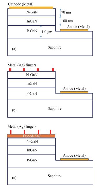
Fig. 1.
(a), (b), (c) Schematic of GaN/InGaN solar cell with metal (Ag) film and metal fingers electrode and metal (Ag)-fingers/doped-ZnO electrodes respectively.
SEMICONDUCTOR PHYSICS
Corresponding author: S. R. Routray, Email: t.r.lenka@ieee.org
Abstract: The effect of doped-ZnO transparent conductive oxide (TCO) with metal (Ag)-fingers contact on GaN/InGaN solar cell is investigated through numerical simulations. An optical and electrical analysis of different dopant elements (such as B, Al, Ga, In and Sn) with ZnO as a top TCO layer is studied. A comparative analysis of metal square pad electrode, metal grid pattern electrode and metal-finger/ZnO type electrodes are taken into consideration to ensure the effect of anti-reflectivity by ZnO. The effect of thickness of ZnO and i-InGaN layer on performance of solar cell is also studied in detail. The proposed solar cell structure with Ag-fingers/ZnO:Al as top contact electrode shows interesting device characteristics compared to other dopants and metal top electrodes. The device achieves open circuit voltage~2.525 V, short circuit current~4.256 mA/cm2, fill factor~87.86% and efficiency~9.22% under 1 Sun, air mass 1.5 global illumination.
Keywords: Ag-finger/doped-ZnO TCO, resistivity, dopants, GaN/InGaN solar cell
| [1] |
Mclaughlin D V P, Pearce J M. Progress in indium gallium nitride materials for solar photovoltaic energy conversion. Metall Mater Trans A, 2013, 44A(44):1947 doi: 10.1007/s11661-013-1622-1
|
| [2] |
Jiang L R, Liu J P, Tian A Q, et al. GaN-based green laser diodes. J Semicond, 2016, 37(11):111001 doi: 10.1088/1674-4926/37/11/111001
|
| [3] |
Zhang H, Messanvi A, Durand C, et al. InGaN/GaN core/shell nanowires for visible to ultraviolet range photodetection. Phys Status Solidi Appl Mater Sci, 2016, 940(4):936 doi: 10.1002/pssa.201532573/abstract
|
| [4] |
Qian F, Li Y, Gradecak S, et al. Multi-quantum-well nanowire heterostructures for wavelength-controlled lasers. Nat Mater, 2008, 7(9):701 doi: 10.1038/nmat2253
|
| [5] |
Green M A, Emery K, Hishikawa Y, et al. Solar cell efficiency tables (version 48). Prog Photovolt Res, 2016, 24(7):905 doi: 10.1002/pip.v24.7
|
| [6] |
Lin M, Xu Y X, Zhang J H, et al. Hybrid functional calculations on the band gap bowing parameters of InxGa1-xN. J Semicond, 2016, 37(4):42001 doi: 10.1088/1674-4926/37/4/042001
|
| [7] |
Jing L, Xiao H L, Wang X L, et al. Enhanced performance of InGaN/GaN multiple quantum well solar cells with patterned sapphire substrate. J Semicond, 2013, 34(12):24004 http://d.wanfangdata.com.cn/Periodical/bdtxb201312010
|
| [8] |
Wu J, Walukiewicz W, Yu K M, et al. Superior radiation resistance of In1-xGaxN alloys:full-solar-spectrum photovoltaic material system. J Appl Phys, 2003, 94(10):6477 doi: 10.1063/1.1618353
|
| [9] |
Hamzaoui H, Bouazzi A S, Rezig B. Theoretical possibilities of InxGa1-xN tandem PV structures. Sol Energy Mater Sol Cells, 2005, 87(1-4):595 doi: 10.1016/j.solmat.2004.08.020
|
| [10] |
Chang J Y, Yen S H, Chang Y A, et al. Numerical investigation of high-efficiency InGaN-based multi-junction solar cell. IEEE Trans Electron Devices, 2013, 60(12):4140 doi: 10.1109/TED.2013.2285573
|
| [11] |
Cai X, Wang Y, Chen B, et al. Investigation of InGaN p-i-n homojunction and heterojunction solar cells. IEEE Photon Technol Lett, 2013, 25(1):59 doi: 10.1109/LPT.2012.2227702
|
| [12] |
Jani O, Honsberg C, Huang Y, et al. Design, growth, fabrication and characterization of high-band gap InGaN/GaN solar cells. WCPEC, 2006:20 http://ieeexplore.ieee.org/document/4059552/
|
| [13] |
Liou B W. InxGa1-xN-GaN-based solar cells with a multiple quantum-well structure on SiCN-Si (111) substrates. Thin Solid Film, 2011, 520(3):1084 doi: 10.1016/j.tsf.2011.01.086
|
| [14] |
Bhuiyan A G, Sugita K, Hashimoto A, et al. InGaN solar cells:Present state of the art and important challenges. IEEE J Photovoltaics, 2012, 2(3):276 doi: 10.1109/JPHOTOV.2012.2193384
|
| [15] |
Chang J Y, Kuo Y K. Numerical study on the influence of piezoelectric polarization on the performance of p-on-n (0001)-face GaN/InGaN p-i-n solar cells. IEEE Electron Device Lett, 2011, 32(7):937 doi: 10.1109/LED.2011.2150195
|
| [16] |
Dickerson J R, Pantzas K, Ougazzaden A, et al. Polarization-induced electric fields make robust n-GaN/i-InGaN/p-GaN solar cells. IEEE Electron Device Lett, 2013, 34(3):363 doi: 10.1109/LED.2012.2237376
|
| [17] |
Hartlieb P J, Roskowski A, Davis R F, et al. Chemical, electrical, and structural properties of Ni/Au contacts on chemical vapor cleaned p-type GaN. J Appl Phys, 2002, 91(11):9151 doi: 10.1063/1.1471578
|
| [18] |
Arai T, Sueyoshi H, Koide Y, et al. Development of Pt-based ohmic contact materials for p-type GaN. J Appl Phys, 2001, 89(5):2826 doi: 10.1063/1.1344578
|
| [19] |
Zhou L, Lanford W, Ping A T, et al. Low resistance Ti/Pt/Au ohmic contacts to p-type GaN. Appl Phys Lett, 2000, 76(23):3451 doi: 10.1063/1.126674
|
| [20] |
Kim T W, Choo D C, No Y S, et al. High work function of Al-doped zinc-oxide thin films as transparent conductive anodes in organic light-emitting devices. Appl Surf Sci, 2006, 253(4):1917 doi: 10.1016/j.apsusc.2006.03.032
|
| [21] |
Minami T. Transparent conducting oxide semiconductors for transparent electrodes. Semi Sci Technol, 2005, 20(4):35 doi: 10.1088/0268-1242/20/4/004
|
| [22] |
Krc C J, Malmstrom J, Edoff M, et al. The potential of textured front ZnO and flat TCO/metal back contact to improve optical absorption in thin Cu(In, Ga)Se2 solar cells. Thin solid films, 2007, 515(15):5968 doi: 10.1016/j.tsf.2006.12.093
|
| [23] |
Hartnagel H L, Dawar A L, Jain A K, et al. Semiconducting transparent thin films. Bristol:Institute of Physics Publishing, 1995
|
| [24] |
Ellmer K. Past achievements and future challenges in the development of optically transparent electrodes. Nat Photonics, 2012, 6:809 doi: 10.1038/nphoton.2012.282
|
| [25] |
Tun C J, Sheu J K, Pong B J, et al. Enhanced light output of GaN-based power LEDs with transparent Al-doped ZnO current spreading layer. IEEE Photonics Technol Lett, 2006, 18(1):274 doi: 10.1109/LPT.2005.861987
|
| [26] |
Kang D W, Kwon J Y, Shim J, et al. Highly conductive GaN anti-reflection layer at transparent conducting oxide/Si interface for silicon thin film solar cells. Sol Energy Mater Sol C, 2012, 105:317 doi: 10.1016/j.solmat.2012.06.041
|
| [27] |
Victory Device User's Manual. California: Silvaco International, 2015
|
| [28] |
Maldonado F, Stashans A. Al-doped ZnO:electronic, electrical and structural properties. J Phys Chem Solids, 2010, 71(5):784 doi: 10.1016/j.jpcs.2010.02.001
|
| [29] |
Kumar V, Singh R G, Purohit L P, et al. Structural, transport and optical properties of boron-doped zinc oxide nanocrystalline. J Mater Sci Technol, 2011, 27(6):481 doi: 10.1016/S1005-0302(11)60095-9
|
| [30] |
Hsieh J H, Chang C K, Hsieh H H, et al. Electrical and optical properties of gallium-doped zinc oxide thin films prepared by ion-beam-assisted deposition. Vaccum, 2015, 118:43 doi: 10.1016/j.vacuum.2015.02.034
|
| [31] |
Biswal R, Maldonado A, Vega-Pérez J, et al. Indium doped zinc oxide thin films deposited by ultrasonic chemical spray technique starting from zinc acetylacetonate and indium chloride. Materials, 2014, 7:5038 doi: 10.3390/ma7075038
|
| [32] |
Bedia F Z, Bedia A, Aillerie M, et al. Structural, optical and electrical properties of Sn-doped zinc oxide transparent films interesting for organic solar cells (OSCs). TMREES15, 2015:539 http://www.sciencedirect.com/science/article/pii/S1876610215015131
|
| [33] |
Liu Y, Li Y, Zeng H. ZnO-based transparent conductive thin films:doping, performance, and processing. J Nanomater, 2013, 2013:1 http://connection.ebscohost.com/c/articles/95401246/zno-based-transparent-conductive-thin-films-doping-performance-processing
|
| [34] |
Holec D, Costa P M F J, Kappers M J, et al. Critical thickness calculations for InGaN/GaN. J Cryst Growth, 2007, 303:314 doi: 10.1016/j.jcrysgro.2006.12.054
|
| [35] |
Kuo Y K, Chang J Y, Shih Y H. Numerical study of the effects of hetero-interfaces, polarization charges, and step-graded interlayers on the photovoltaic properties of (0001) face GaN/InGaN p-i-n solar cell. IEEE J Quantum Electron, 2012, 48(3):367 doi: 10.1109/JQE.2011.2181972
|
| [36] |
Walukiewicz W, Ager J W, Yu K M, et al. Structure and electronic properties of InN and in-rich group Ⅲ-nitride alloys. J Phys D, 2006, 39:R83 doi: 10.1088/0022-3727/39/5/R01
|
| [37] |
Fiorentini V, Bernardini F, Ambacher O. Evidence for nonlinear macroscopic polarization in Ⅲ-Ⅴ nitride alloy heterostructures. Appl Phys Lett, 2002, 80(7):1204 doi: 10.1063/1.1448668
|
| [38] |
Brown G F, Ager J W, Walukiewicz W, et al. Finite element simulations of compositionally graded InGaN solar cells. Sol Energy Mater Sol Cells, 2010, 94(3):478 doi: 10.1016/j.solmat.2009.11.010
|
| [39] |
Li Z Q, Lestradet M, Xiao Y G, et al. Effects of polarization charge on the photovoltaic properties of InGaN solar cells. Phys Status Solidi Appl Mater Sci, 2011, 208(4):928 doi: 10.1002/pssa.v208.4
|
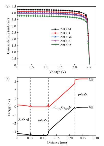
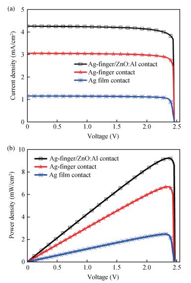
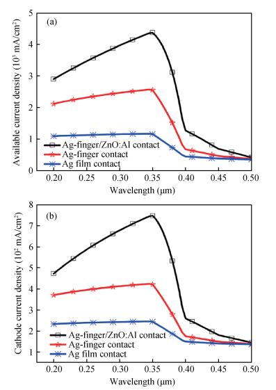
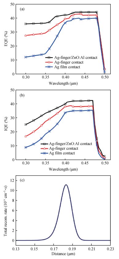
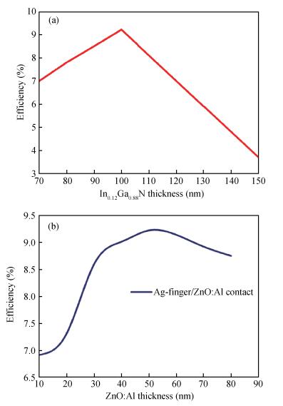
Table 3. Measuring parameters of GaN/InGaN solar cell with different types of contacts.

|
 DownLoad: CSV
| [1] |
Mclaughlin D V P, Pearce J M. Progress in indium gallium nitride materials for solar photovoltaic energy conversion. Metall Mater Trans A, 2013, 44A(44):1947 doi: 10.1007/s11661-013-1622-1
|
| [2] |
Jiang L R, Liu J P, Tian A Q, et al. GaN-based green laser diodes. J Semicond, 2016, 37(11):111001 doi: 10.1088/1674-4926/37/11/111001
|
| [3] |
Zhang H, Messanvi A, Durand C, et al. InGaN/GaN core/shell nanowires for visible to ultraviolet range photodetection. Phys Status Solidi Appl Mater Sci, 2016, 940(4):936 doi: 10.1002/pssa.201532573/abstract
|
| [4] |
Qian F, Li Y, Gradecak S, et al. Multi-quantum-well nanowire heterostructures for wavelength-controlled lasers. Nat Mater, 2008, 7(9):701 doi: 10.1038/nmat2253
|
| [5] |
Green M A, Emery K, Hishikawa Y, et al. Solar cell efficiency tables (version 48). Prog Photovolt Res, 2016, 24(7):905 doi: 10.1002/pip.v24.7
|
| [6] |
Lin M, Xu Y X, Zhang J H, et al. Hybrid functional calculations on the band gap bowing parameters of InxGa1-xN. J Semicond, 2016, 37(4):42001 doi: 10.1088/1674-4926/37/4/042001
|
| [7] |
Jing L, Xiao H L, Wang X L, et al. Enhanced performance of InGaN/GaN multiple quantum well solar cells with patterned sapphire substrate. J Semicond, 2013, 34(12):24004 http://d.wanfangdata.com.cn/Periodical/bdtxb201312010
|
| [8] |
Wu J, Walukiewicz W, Yu K M, et al. Superior radiation resistance of In1-xGaxN alloys:full-solar-spectrum photovoltaic material system. J Appl Phys, 2003, 94(10):6477 doi: 10.1063/1.1618353
|
| [9] |
Hamzaoui H, Bouazzi A S, Rezig B. Theoretical possibilities of InxGa1-xN tandem PV structures. Sol Energy Mater Sol Cells, 2005, 87(1-4):595 doi: 10.1016/j.solmat.2004.08.020
|
| [10] |
Chang J Y, Yen S H, Chang Y A, et al. Numerical investigation of high-efficiency InGaN-based multi-junction solar cell. IEEE Trans Electron Devices, 2013, 60(12):4140 doi: 10.1109/TED.2013.2285573
|
| [11] |
Cai X, Wang Y, Chen B, et al. Investigation of InGaN p-i-n homojunction and heterojunction solar cells. IEEE Photon Technol Lett, 2013, 25(1):59 doi: 10.1109/LPT.2012.2227702
|
| [12] |
Jani O, Honsberg C, Huang Y, et al. Design, growth, fabrication and characterization of high-band gap InGaN/GaN solar cells. WCPEC, 2006:20 http://ieeexplore.ieee.org/document/4059552/
|
| [13] |
Liou B W. InxGa1-xN-GaN-based solar cells with a multiple quantum-well structure on SiCN-Si (111) substrates. Thin Solid Film, 2011, 520(3):1084 doi: 10.1016/j.tsf.2011.01.086
|
| [14] |
Bhuiyan A G, Sugita K, Hashimoto A, et al. InGaN solar cells:Present state of the art and important challenges. IEEE J Photovoltaics, 2012, 2(3):276 doi: 10.1109/JPHOTOV.2012.2193384
|
| [15] |
Chang J Y, Kuo Y K. Numerical study on the influence of piezoelectric polarization on the performance of p-on-n (0001)-face GaN/InGaN p-i-n solar cells. IEEE Electron Device Lett, 2011, 32(7):937 doi: 10.1109/LED.2011.2150195
|
| [16] |
Dickerson J R, Pantzas K, Ougazzaden A, et al. Polarization-induced electric fields make robust n-GaN/i-InGaN/p-GaN solar cells. IEEE Electron Device Lett, 2013, 34(3):363 doi: 10.1109/LED.2012.2237376
|
| [17] |
Hartlieb P J, Roskowski A, Davis R F, et al. Chemical, electrical, and structural properties of Ni/Au contacts on chemical vapor cleaned p-type GaN. J Appl Phys, 2002, 91(11):9151 doi: 10.1063/1.1471578
|
| [18] |
Arai T, Sueyoshi H, Koide Y, et al. Development of Pt-based ohmic contact materials for p-type GaN. J Appl Phys, 2001, 89(5):2826 doi: 10.1063/1.1344578
|
| [19] |
Zhou L, Lanford W, Ping A T, et al. Low resistance Ti/Pt/Au ohmic contacts to p-type GaN. Appl Phys Lett, 2000, 76(23):3451 doi: 10.1063/1.126674
|
| [20] |
Kim T W, Choo D C, No Y S, et al. High work function of Al-doped zinc-oxide thin films as transparent conductive anodes in organic light-emitting devices. Appl Surf Sci, 2006, 253(4):1917 doi: 10.1016/j.apsusc.2006.03.032
|
| [21] |
Minami T. Transparent conducting oxide semiconductors for transparent electrodes. Semi Sci Technol, 2005, 20(4):35 doi: 10.1088/0268-1242/20/4/004
|
| [22] |
Krc C J, Malmstrom J, Edoff M, et al. The potential of textured front ZnO and flat TCO/metal back contact to improve optical absorption in thin Cu(In, Ga)Se2 solar cells. Thin solid films, 2007, 515(15):5968 doi: 10.1016/j.tsf.2006.12.093
|
| [23] |
Hartnagel H L, Dawar A L, Jain A K, et al. Semiconducting transparent thin films. Bristol:Institute of Physics Publishing, 1995
|
| [24] |
Ellmer K. Past achievements and future challenges in the development of optically transparent electrodes. Nat Photonics, 2012, 6:809 doi: 10.1038/nphoton.2012.282
|
| [25] |
Tun C J, Sheu J K, Pong B J, et al. Enhanced light output of GaN-based power LEDs with transparent Al-doped ZnO current spreading layer. IEEE Photonics Technol Lett, 2006, 18(1):274 doi: 10.1109/LPT.2005.861987
|
| [26] |
Kang D W, Kwon J Y, Shim J, et al. Highly conductive GaN anti-reflection layer at transparent conducting oxide/Si interface for silicon thin film solar cells. Sol Energy Mater Sol C, 2012, 105:317 doi: 10.1016/j.solmat.2012.06.041
|
| [27] |
Victory Device User's Manual. California: Silvaco International, 2015
|
| [28] |
Maldonado F, Stashans A. Al-doped ZnO:electronic, electrical and structural properties. J Phys Chem Solids, 2010, 71(5):784 doi: 10.1016/j.jpcs.2010.02.001
|
| [29] |
Kumar V, Singh R G, Purohit L P, et al. Structural, transport and optical properties of boron-doped zinc oxide nanocrystalline. J Mater Sci Technol, 2011, 27(6):481 doi: 10.1016/S1005-0302(11)60095-9
|
| [30] |
Hsieh J H, Chang C K, Hsieh H H, et al. Electrical and optical properties of gallium-doped zinc oxide thin films prepared by ion-beam-assisted deposition. Vaccum, 2015, 118:43 doi: 10.1016/j.vacuum.2015.02.034
|
| [31] |
Biswal R, Maldonado A, Vega-Pérez J, et al. Indium doped zinc oxide thin films deposited by ultrasonic chemical spray technique starting from zinc acetylacetonate and indium chloride. Materials, 2014, 7:5038 doi: 10.3390/ma7075038
|
| [32] |
Bedia F Z, Bedia A, Aillerie M, et al. Structural, optical and electrical properties of Sn-doped zinc oxide transparent films interesting for organic solar cells (OSCs). TMREES15, 2015:539 http://www.sciencedirect.com/science/article/pii/S1876610215015131
|
| [33] |
Liu Y, Li Y, Zeng H. ZnO-based transparent conductive thin films:doping, performance, and processing. J Nanomater, 2013, 2013:1 http://connection.ebscohost.com/c/articles/95401246/zno-based-transparent-conductive-thin-films-doping-performance-processing
|
| [34] |
Holec D, Costa P M F J, Kappers M J, et al. Critical thickness calculations for InGaN/GaN. J Cryst Growth, 2007, 303:314 doi: 10.1016/j.jcrysgro.2006.12.054
|
| [35] |
Kuo Y K, Chang J Y, Shih Y H. Numerical study of the effects of hetero-interfaces, polarization charges, and step-graded interlayers on the photovoltaic properties of (0001) face GaN/InGaN p-i-n solar cell. IEEE J Quantum Electron, 2012, 48(3):367 doi: 10.1109/JQE.2011.2181972
|
| [36] |
Walukiewicz W, Ager J W, Yu K M, et al. Structure and electronic properties of InN and in-rich group Ⅲ-nitride alloys. J Phys D, 2006, 39:R83 doi: 10.1088/0022-3727/39/5/R01
|
| [37] |
Fiorentini V, Bernardini F, Ambacher O. Evidence for nonlinear macroscopic polarization in Ⅲ-Ⅴ nitride alloy heterostructures. Appl Phys Lett, 2002, 80(7):1204 doi: 10.1063/1.1448668
|
| [38] |
Brown G F, Ager J W, Walukiewicz W, et al. Finite element simulations of compositionally graded InGaN solar cells. Sol Energy Mater Sol Cells, 2010, 94(3):478 doi: 10.1016/j.solmat.2009.11.010
|
| [39] |
Li Z Q, Lestradet M, Xiao Y G, et al. Effects of polarization charge on the photovoltaic properties of InGaN solar cells. Phys Status Solidi Appl Mater Sci, 2011, 208(4):928 doi: 10.1002/pssa.v208.4
|


Article views: 6159 Times PDF downloads: 48 Times Cited by: 0 Times
Received: 20 January 2017 Revised: 07 March 2017 Online: Published: 01 September 2017
| Citation: |
S.R. Routray, T.R. Lenka. Effect of metal-fingers/doped-ZnO transparent electrode on performance of GaN/InGaN solar cell[J]. Journal of Semiconductors, 2017, 38(9): 092001. doi: 10.1088/1674-4926/38/9/092001
****
S R Routray, T R Lenka. Effect of metal-fingers/doped-ZnO transparent electrode on performance of GaN/InGaN solar cell[J]. J. Semicond., 2017, 38(9): 092001. doi: 10.1088/1674-4926/38/9/092001.

|
| [1] |
Mclaughlin D V P, Pearce J M. Progress in indium gallium nitride materials for solar photovoltaic energy conversion. Metall Mater Trans A, 2013, 44A(44):1947 doi: 10.1007/s11661-013-1622-1
|
| [2] |
Jiang L R, Liu J P, Tian A Q, et al. GaN-based green laser diodes. J Semicond, 2016, 37(11):111001 doi: 10.1088/1674-4926/37/11/111001
|
| [3] |
Zhang H, Messanvi A, Durand C, et al. InGaN/GaN core/shell nanowires for visible to ultraviolet range photodetection. Phys Status Solidi Appl Mater Sci, 2016, 940(4):936 doi: 10.1002/pssa.201532573/abstract
|
| [4] |
Qian F, Li Y, Gradecak S, et al. Multi-quantum-well nanowire heterostructures for wavelength-controlled lasers. Nat Mater, 2008, 7(9):701 doi: 10.1038/nmat2253
|
| [5] |
Green M A, Emery K, Hishikawa Y, et al. Solar cell efficiency tables (version 48). Prog Photovolt Res, 2016, 24(7):905 doi: 10.1002/pip.v24.7
|
| [6] |
Lin M, Xu Y X, Zhang J H, et al. Hybrid functional calculations on the band gap bowing parameters of InxGa1-xN. J Semicond, 2016, 37(4):42001 doi: 10.1088/1674-4926/37/4/042001
|
| [7] |
Jing L, Xiao H L, Wang X L, et al. Enhanced performance of InGaN/GaN multiple quantum well solar cells with patterned sapphire substrate. J Semicond, 2013, 34(12):24004 http://d.wanfangdata.com.cn/Periodical/bdtxb201312010
|
| [8] |
Wu J, Walukiewicz W, Yu K M, et al. Superior radiation resistance of In1-xGaxN alloys:full-solar-spectrum photovoltaic material system. J Appl Phys, 2003, 94(10):6477 doi: 10.1063/1.1618353
|
| [9] |
Hamzaoui H, Bouazzi A S, Rezig B. Theoretical possibilities of InxGa1-xN tandem PV structures. Sol Energy Mater Sol Cells, 2005, 87(1-4):595 doi: 10.1016/j.solmat.2004.08.020
|
| [10] |
Chang J Y, Yen S H, Chang Y A, et al. Numerical investigation of high-efficiency InGaN-based multi-junction solar cell. IEEE Trans Electron Devices, 2013, 60(12):4140 doi: 10.1109/TED.2013.2285573
|
| [11] |
Cai X, Wang Y, Chen B, et al. Investigation of InGaN p-i-n homojunction and heterojunction solar cells. IEEE Photon Technol Lett, 2013, 25(1):59 doi: 10.1109/LPT.2012.2227702
|
| [12] |
Jani O, Honsberg C, Huang Y, et al. Design, growth, fabrication and characterization of high-band gap InGaN/GaN solar cells. WCPEC, 2006:20 http://ieeexplore.ieee.org/document/4059552/
|
| [13] |
Liou B W. InxGa1-xN-GaN-based solar cells with a multiple quantum-well structure on SiCN-Si (111) substrates. Thin Solid Film, 2011, 520(3):1084 doi: 10.1016/j.tsf.2011.01.086
|
| [14] |
Bhuiyan A G, Sugita K, Hashimoto A, et al. InGaN solar cells:Present state of the art and important challenges. IEEE J Photovoltaics, 2012, 2(3):276 doi: 10.1109/JPHOTOV.2012.2193384
|
| [15] |
Chang J Y, Kuo Y K. Numerical study on the influence of piezoelectric polarization on the performance of p-on-n (0001)-face GaN/InGaN p-i-n solar cells. IEEE Electron Device Lett, 2011, 32(7):937 doi: 10.1109/LED.2011.2150195
|
| [16] |
Dickerson J R, Pantzas K, Ougazzaden A, et al. Polarization-induced electric fields make robust n-GaN/i-InGaN/p-GaN solar cells. IEEE Electron Device Lett, 2013, 34(3):363 doi: 10.1109/LED.2012.2237376
|
| [17] |
Hartlieb P J, Roskowski A, Davis R F, et al. Chemical, electrical, and structural properties of Ni/Au contacts on chemical vapor cleaned p-type GaN. J Appl Phys, 2002, 91(11):9151 doi: 10.1063/1.1471578
|
| [18] |
Arai T, Sueyoshi H, Koide Y, et al. Development of Pt-based ohmic contact materials for p-type GaN. J Appl Phys, 2001, 89(5):2826 doi: 10.1063/1.1344578
|
| [19] |
Zhou L, Lanford W, Ping A T, et al. Low resistance Ti/Pt/Au ohmic contacts to p-type GaN. Appl Phys Lett, 2000, 76(23):3451 doi: 10.1063/1.126674
|
| [20] |
Kim T W, Choo D C, No Y S, et al. High work function of Al-doped zinc-oxide thin films as transparent conductive anodes in organic light-emitting devices. Appl Surf Sci, 2006, 253(4):1917 doi: 10.1016/j.apsusc.2006.03.032
|
| [21] |
Minami T. Transparent conducting oxide semiconductors for transparent electrodes. Semi Sci Technol, 2005, 20(4):35 doi: 10.1088/0268-1242/20/4/004
|
| [22] |
Krc C J, Malmstrom J, Edoff M, et al. The potential of textured front ZnO and flat TCO/metal back contact to improve optical absorption in thin Cu(In, Ga)Se2 solar cells. Thin solid films, 2007, 515(15):5968 doi: 10.1016/j.tsf.2006.12.093
|
| [23] |
Hartnagel H L, Dawar A L, Jain A K, et al. Semiconducting transparent thin films. Bristol:Institute of Physics Publishing, 1995
|
| [24] |
Ellmer K. Past achievements and future challenges in the development of optically transparent electrodes. Nat Photonics, 2012, 6:809 doi: 10.1038/nphoton.2012.282
|
| [25] |
Tun C J, Sheu J K, Pong B J, et al. Enhanced light output of GaN-based power LEDs with transparent Al-doped ZnO current spreading layer. IEEE Photonics Technol Lett, 2006, 18(1):274 doi: 10.1109/LPT.2005.861987
|
| [26] |
Kang D W, Kwon J Y, Shim J, et al. Highly conductive GaN anti-reflection layer at transparent conducting oxide/Si interface for silicon thin film solar cells. Sol Energy Mater Sol C, 2012, 105:317 doi: 10.1016/j.solmat.2012.06.041
|
| [27] |
Victory Device User's Manual. California: Silvaco International, 2015
|
| [28] |
Maldonado F, Stashans A. Al-doped ZnO:electronic, electrical and structural properties. J Phys Chem Solids, 2010, 71(5):784 doi: 10.1016/j.jpcs.2010.02.001
|
| [29] |
Kumar V, Singh R G, Purohit L P, et al. Structural, transport and optical properties of boron-doped zinc oxide nanocrystalline. J Mater Sci Technol, 2011, 27(6):481 doi: 10.1016/S1005-0302(11)60095-9
|
| [30] |
Hsieh J H, Chang C K, Hsieh H H, et al. Electrical and optical properties of gallium-doped zinc oxide thin films prepared by ion-beam-assisted deposition. Vaccum, 2015, 118:43 doi: 10.1016/j.vacuum.2015.02.034
|
| [31] |
Biswal R, Maldonado A, Vega-Pérez J, et al. Indium doped zinc oxide thin films deposited by ultrasonic chemical spray technique starting from zinc acetylacetonate and indium chloride. Materials, 2014, 7:5038 doi: 10.3390/ma7075038
|
| [32] |
Bedia F Z, Bedia A, Aillerie M, et al. Structural, optical and electrical properties of Sn-doped zinc oxide transparent films interesting for organic solar cells (OSCs). TMREES15, 2015:539 http://www.sciencedirect.com/science/article/pii/S1876610215015131
|
| [33] |
Liu Y, Li Y, Zeng H. ZnO-based transparent conductive thin films:doping, performance, and processing. J Nanomater, 2013, 2013:1 http://connection.ebscohost.com/c/articles/95401246/zno-based-transparent-conductive-thin-films-doping-performance-processing
|
| [34] |
Holec D, Costa P M F J, Kappers M J, et al. Critical thickness calculations for InGaN/GaN. J Cryst Growth, 2007, 303:314 doi: 10.1016/j.jcrysgro.2006.12.054
|
| [35] |
Kuo Y K, Chang J Y, Shih Y H. Numerical study of the effects of hetero-interfaces, polarization charges, and step-graded interlayers on the photovoltaic properties of (0001) face GaN/InGaN p-i-n solar cell. IEEE J Quantum Electron, 2012, 48(3):367 doi: 10.1109/JQE.2011.2181972
|
| [36] |
Walukiewicz W, Ager J W, Yu K M, et al. Structure and electronic properties of InN and in-rich group Ⅲ-nitride alloys. J Phys D, 2006, 39:R83 doi: 10.1088/0022-3727/39/5/R01
|
| [37] |
Fiorentini V, Bernardini F, Ambacher O. Evidence for nonlinear macroscopic polarization in Ⅲ-Ⅴ nitride alloy heterostructures. Appl Phys Lett, 2002, 80(7):1204 doi: 10.1063/1.1448668
|
| [38] |
Brown G F, Ager J W, Walukiewicz W, et al. Finite element simulations of compositionally graded InGaN solar cells. Sol Energy Mater Sol Cells, 2010, 94(3):478 doi: 10.1016/j.solmat.2009.11.010
|
| [39] |
Li Z Q, Lestradet M, Xiao Y G, et al. Effects of polarization charge on the photovoltaic properties of InGaN solar cells. Phys Status Solidi Appl Mater Sci, 2011, 208(4):928 doi: 10.1002/pssa.v208.4
|
 2017年中国高校科技期刊“优秀团队及优秀个人”入选名单.xlsx
|

|

 WeChat ID
Journal of Semiconductors © 2017 All Rights Reserved 京ICP备05085259号-2


