Fig. 1.
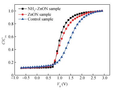
Normalized HF (1 MHz) C-V curve of the three samples
SEMICONDUCTOR DEVICES
Jingkang Gong, Jingping Xu, Lu Liu, Hanhan Lu, Xiaoyu Liu and Yaoyao Feng
Corresponding author: Jingping Xu Email: jpxu@mail.hust.edu.cn
Abstract: The GaAs MOS capacitor was fabricated with HfTiON as high-k gate dielectric and NH3-plasma-treated ZnON as interfacial passivation layer (IPL), and its interfacial and electrical properties are investigated compared to its counterparts with ZnON IPL but no NH3-plasma treatment and without ZnON IPL and no plasma treatment. Experimental results show that low interface-state density near midgap (1.17×1012 cm-2eV-1) and small gate leakage current density have been achieved for the GaAs MOS device with the stacked gate dielectric of HfTiON/ZnON plus NH3-plasma treatment. These improvements could be ascribed to the fact that the ZnON IPL can effectively block in-diffusion of oxygen atoms and out-diffusion of Ga and As atoms, and the NH3-plasma treatment can provide not only N atoms but also H atoms and NH radicals, which is greatly beneficial to removal of defective Ga/As oxides and As-As band, giving a high-quality ZnON/GaAs interface.
Keywords: GaAs MOS, ZnON interfacial passivation layer, NH3-plasma treatment
| [1] |
He G, Chen X, Sun Z. Interface engineering and chemistry of Hf-based high-k dielectrics on Ⅲ-V substrates. Surf Sci Rep, 2013, 68(1):68 doi: 10.1016/j.surfrep.2013.01.002
|
| [2] |
Suzuki R, Taoka N, Yokoyama M, et al. 1-nm-capacitance-equivalent-thickness HfO2/Al2O3/InGaAs metal-oxide-semiconductor structure with low interface trap density and low gate leakage current density. Appl Phys Lett, 2012, 100(13):132906 doi: 10.1063/1.3698095
|
| [3] |
Das P S, Biswas A. Investigations on electrical characteristics and reliability properties of MOS capacitors using HfAlOx on n-GaAs substrates. Microelectron Reliab, 2012, 52(1):112 doi: 10.1016/j.microrel.2011.08.005
|
| [4] |
Kundu S, Roy S, Banerji P, et al. Studies on Al/ZrO2/GaAs metal-oxide-semiconductor capacitors and determination of its electrical parameters in the frequency range of 10 kHz-1 MHz. J Vac Sci Technol B, 2011, 29(3):1203 http://independent.academia.edu/souvikkundu1
|
| [5] |
Ji F, Xu J P, Liu J G, et al. Improved interface properties of Ge metal-oxide-semiconductor capacitor with TaTiO gate dielectric by using in situ TaON passivation interlayer. Appl Phys Lett, 2011, 98(18):182901 doi: 10.1063/1.3581891
|
| [6] |
Passlack M, Medendorp N, Gregory R, et al. Role of Ga2O3 template thickness and gadolinium mole fraction in GdxGa0.4-xO0.6/Ga2O3 gate dielectric stacks on GaAs. Appl Phys Lett, 2003, 83(25):5262 doi: 10.1063/1.1635068
|
| [7] |
Wang L S, Xu J P, Zhu S Y, et al. Improved interfacial and electrical properties of GaAs metal-oxide-semiconductor capacitors with HfTiON as gate dielectric and TaON as passivation interlayer. Appl Phys Lett, 2013, 103(9):112901 http://hub.hku.hk/bitstream/10722/202921/1/Content.pdf?accept=1
|
| [8] |
Shahrjerdi D, Oye M M, Holmes A L Jr, et al. Unpinned metal gate/high-k GaAs capacitors:fabrication and characterization. Appl Phys Lett, 2006, 89(4):49 doi: 10.1063/1.2234837?journalCode=apl
|
| [9] |
Liu C, Zhang Y M, Zhang Y M, et al. Interfacial characteristics of Al/Al2O3/ZnO/n-GaAs MOS capacitor. Chin Phys B, 2013, 22(7):406 http://kns.cnki.net/KCMS/detail/detail.aspx?filename=zgwl201307070&dbname=CJFD&dbcode=CJFQ
|
| [10] |
Kundu S, Shripathi T, Banerji P. Interface engineering with an MOCVD grown ZnO interface passivation layer for ZrO2-GaAs metal-oxide-semiconductor devices. Solid State Commun, 2011, 151(24):1881 doi: 10.1016/j.ssc.2011.09.033
|
| [11] |
Lee S, Nathan A, Ye Y, et al. Localized tail states and electron mobility in amorphous ZnON thin film transistors. Sci Rep, 2015, 5:13467 doi: 10.1038/srep13467
|
| [12] |
Ghosh C K, Malkhandi S, Mitra M K, et al. Effect of Ni doping on the dielectric constant of ZnO and its frequency dependent exchange interaction. J Phys D, 2008, 41(41):245113 http://shodhganga.inflibnet.ac.in/bitstream/10603/42983/14/14chapter7.pdf
|
| [13] |
Lu H, Xu J P, Liu L, et al. Improved interfacial quality of GaAs metal-oxide-semiconductor device with NH3-plasma treated yittrium-oxynitride as interfacial passivation layer. Microelectron Reliab, 2016, 56:17 https://dialnet.unirioja.es/servlet/articulo?codigo=5305745
|
| [14] |
Yasui K, Arayama T, Okutani S, et al. Generation of ammonia plasma using a helical antenna and nitridation of GaAs surface. Appl Surf Sci, 2003, 212(2):619 http://cat.inist.fr/?aModele=exportN&cpsidt=14887882
|
| [15] |
O'Connor E, Djara V, Monaghan S, et al. Capacitance-voltage and interface state density characteristics of GaAs and InGaAs MOS capacitors incorporating a PECVD SiN dielectric. ES Trans, 2011, 415:35 https://www.mendeley.com/research-papers/capacitancevoltage-interface-state-density-characteristics-gaas-ingaas-mos-capacitors-incorporating/
|
| [16] |
Losurdo M, Capezzuto P, Bruno G, et al. N2-H2 remote plasma nitridation for GaAs surface passivation. Appl Phys Lett, 2002, 81(1):16 doi: 10.1063/1.1490414
|
| [17] |
Frank M M, Wilk G D, Starodub D, et al. HfO2 and Al2O3 gate dielectrics on GaAs grown by atomic layer deposition. Appl Phys Lett, 2005, 86(15):87 http://www.fujitsu.com/global/documents/about/resources/publications/fstj/archives/vol39-1/paper12.pdf
|
| [18] |
Lu H L, Sun L, Ding S J, et al. Characterization of atomic-layer-deposited Al2O3/GaAs interface improved by NH3 plasma pretreatment. Appl Phys Lett, 2006, 89(15):1897 doi: 10.1063/1.2363145?journalCode=apl
|
| [19] |
Yang T, Xuan Y, Zemlyanov D, et al. Interface studies of GaAs metal-oxide-semiconductor structures using atomic-layer-deposited HfO2/Al2O3 nanolaminate gate dielectric. Appl Phys Lett, 2007, 91(14):1099 http://ieeexplore.ieee.org/document/4829101/
|
| [20] |
Wang L S, Xu J P, Liu L, et al. Plasma-nitrided Ga2O3(Gd2O3) as interfacial passivation layer for InGaAs metal-oxide-semiconductor capacitor with HfTiON gate dielectric. IEEE Trans Electron Devices, 2015, 62(4):1235 doi: 10.1109/TED.2015.2396972
|
| [21] |
Terman L M. An investigation of surface states at a silicon/silicon oxide interface employing metal-oxide-silicon diodes. Solid State Electron, 1962, 5:285 doi: 10.1016/0038-1101(62)90111-9
|
| [22] |
Li C C, Chang-Liao K S, Fu C H, et al. Improved electrical characteristics high-k gated MOS devices with in-situ remote plasma treatment in atomic layer deposition. Microelectron Eng, 2013, 109(6):64 http://www.sciencedirect.com/science/article/pii/S0167931713002773
|
| [23] |
Dasa T, Mahata C, Sutradharb G, et al. Characterization of Ti-based high-k gate dielectrics on GaAs. ECS Trans, 201135:325 http://ma.ecsdl.org/content/MA2011-01/18/1209.short
|
| [24] |
Crupi F, Ciofi C, Germanó A, et al. On the role of interface states in low-voltage leakage currents of metal-oxide-semiconductor structures. Appl Phys Lett, 2002, 80(24):4597 doi: 10.1063/1.1487450
|
| [25] |
Xu H X, Xu J P. Electrical properties of Ge metal-oxide-semiconductor capacitors with high-k La2O3 gate dielectric incorporated by N or/and Ti. J Semicond, 2016, 37(6):77 http://d.wanfangdata.com.cn/Periodical/bdtxb201606011
|
| [26] |
Wang L S, Liu L, Xu J P, et al. Electrical properties of HfTiON gate-dielectric GaAs metal-oxide-semiconductor capacitor with AlON as interlayer. IEEE Trans Electron Devices, 2014, 61:1 doi: 10.1109/TED.2013.2292251
|
| [27] |
Lee S, Nathan A, Ye Y, et al. Localized tail states and electron mobility in amorphous ZnON thin film transistors. Sci Rep, 2015, 5:13467 doi: 10.1038/srep13467
|
| [28] |
Gonbeau D, Guimon C, Pfister-Guillouzo G, et al. XPS study of thin films of titanium oxysulfides. Surf Sci, 1991, 254(1-3):81 doi: 10.1016/0039-6028(91)90640-E
|
| [29] |
Flina B J McIntyre N S. Studies of the UV/ozone oxidation of GaAs using angle-resolved X-ray photoelectron spectroscopy. Surf Interface Anal, 1990, 15:19 doi: 10.1002/(ISSN)1096-9918
|
| [30] |
Sugahara H, Oshima M, Oigawa H, et al. Synchrotron radiation photoemission analysis for (NH4)2Sx-treated GaAs. J Appl Phys, 1991, 69(8):4349 doi: 10.1063/1.348380
|
| [31] |
Liu C W, Xu J P, Liu L, et al. High-gate dielectric GaAs MOS device with LaON as interlayer and NH-plasma surface pretreatment. Chin Phys B, 2015, 24:494 http://cpb.iphy.ac.cn/fileup/PDF/2015-12-127304.pdf
|
| [32] |
Ould-Metidji Y, Bideux L, Baca D, et al. Nitridation of GaAs(100) substrates and Ga/GaAs systems studied by XPS spectroscopy. Appl Surf Sci, 2003, 212(2):614 http://www.sciencedirect.com/science/article/pii/S0169433203003957
|
| [33] |
Zhu S Y, Xu J P, Wang L S, et al. Comparison of interfacial and electrical properties between Al2O3 and ZnO as interface passivation layer of GaAs MOS device with HfTiO gate dielectric. J Semicond, 2015, 36(3):74 doi: 10.1021/am506351u?src=recsys
|
| [34] |
Wu Y C, Chang E Y, Lin Y C, et al. Study of the inversion behaviors of Al2O3/InxGa1-xAs metal-oxide-semiconductor capacitors with different In contents. Solid State Electron, 2010, 54(1):37 doi: 10.1016/j.sse.2009.09.033
|
| [35] |
Yan T, Zhang Y M, Lü H L, et al. Temperature dependent interfacial and electrical characteristics during atomic layer deposition and annealing of HfO2 films in p-GaAs metal-oxide-semiconductor capacitors. J Semicond, 2015, 36(12):124003 doi: 10.1088/1674-4926/36/12/124003
|
| [36] |
Pal S, Bose D N. Fabrication and characterization of GaAs MIS devices with N-rich PEVCD SiN dielectric. Appl Surf Sci, 2001, 181:179 doi: 10.1016/S0169-4332(01)00196-9
|
| [37] |
Marchiori C, Webb D J, Rossel C, et al. H plasma cleaning and a-Si passivation of GaAs for surface channel device applications. J Appl Phys, 2009, 106(11):1245 doi: 10.1063/1.3260251?journalCode=jap
|

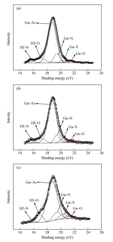
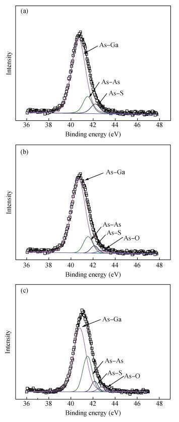
Table 1. Electrical and physical parameters of three samples extracted from their HF C-V curves
 |
| [1] |
He G, Chen X, Sun Z. Interface engineering and chemistry of Hf-based high-k dielectrics on Ⅲ-V substrates. Surf Sci Rep, 2013, 68(1):68 doi: 10.1016/j.surfrep.2013.01.002
|
| [2] |
Suzuki R, Taoka N, Yokoyama M, et al. 1-nm-capacitance-equivalent-thickness HfO2/Al2O3/InGaAs metal-oxide-semiconductor structure with low interface trap density and low gate leakage current density. Appl Phys Lett, 2012, 100(13):132906 doi: 10.1063/1.3698095
|
| [3] |
Das P S, Biswas A. Investigations on electrical characteristics and reliability properties of MOS capacitors using HfAlOx on n-GaAs substrates. Microelectron Reliab, 2012, 52(1):112 doi: 10.1016/j.microrel.2011.08.005
|
| [4] |
Kundu S, Roy S, Banerji P, et al. Studies on Al/ZrO2/GaAs metal-oxide-semiconductor capacitors and determination of its electrical parameters in the frequency range of 10 kHz-1 MHz. J Vac Sci Technol B, 2011, 29(3):1203 http://independent.academia.edu/souvikkundu1
|
| [5] |
Ji F, Xu J P, Liu J G, et al. Improved interface properties of Ge metal-oxide-semiconductor capacitor with TaTiO gate dielectric by using in situ TaON passivation interlayer. Appl Phys Lett, 2011, 98(18):182901 doi: 10.1063/1.3581891
|
| [6] |
Passlack M, Medendorp N, Gregory R, et al. Role of Ga2O3 template thickness and gadolinium mole fraction in GdxGa0.4-xO0.6/Ga2O3 gate dielectric stacks on GaAs. Appl Phys Lett, 2003, 83(25):5262 doi: 10.1063/1.1635068
|
| [7] |
Wang L S, Xu J P, Zhu S Y, et al. Improved interfacial and electrical properties of GaAs metal-oxide-semiconductor capacitors with HfTiON as gate dielectric and TaON as passivation interlayer. Appl Phys Lett, 2013, 103(9):112901 http://hub.hku.hk/bitstream/10722/202921/1/Content.pdf?accept=1
|
| [8] |
Shahrjerdi D, Oye M M, Holmes A L Jr, et al. Unpinned metal gate/high-k GaAs capacitors:fabrication and characterization. Appl Phys Lett, 2006, 89(4):49 doi: 10.1063/1.2234837?journalCode=apl
|
| [9] |
Liu C, Zhang Y M, Zhang Y M, et al. Interfacial characteristics of Al/Al2O3/ZnO/n-GaAs MOS capacitor. Chin Phys B, 2013, 22(7):406 http://kns.cnki.net/KCMS/detail/detail.aspx?filename=zgwl201307070&dbname=CJFD&dbcode=CJFQ
|
| [10] |
Kundu S, Shripathi T, Banerji P. Interface engineering with an MOCVD grown ZnO interface passivation layer for ZrO2-GaAs metal-oxide-semiconductor devices. Solid State Commun, 2011, 151(24):1881 doi: 10.1016/j.ssc.2011.09.033
|
| [11] |
Lee S, Nathan A, Ye Y, et al. Localized tail states and electron mobility in amorphous ZnON thin film transistors. Sci Rep, 2015, 5:13467 doi: 10.1038/srep13467
|
| [12] |
Ghosh C K, Malkhandi S, Mitra M K, et al. Effect of Ni doping on the dielectric constant of ZnO and its frequency dependent exchange interaction. J Phys D, 2008, 41(41):245113 http://shodhganga.inflibnet.ac.in/bitstream/10603/42983/14/14chapter7.pdf
|
| [13] |
Lu H, Xu J P, Liu L, et al. Improved interfacial quality of GaAs metal-oxide-semiconductor device with NH3-plasma treated yittrium-oxynitride as interfacial passivation layer. Microelectron Reliab, 2016, 56:17 https://dialnet.unirioja.es/servlet/articulo?codigo=5305745
|
| [14] |
Yasui K, Arayama T, Okutani S, et al. Generation of ammonia plasma using a helical antenna and nitridation of GaAs surface. Appl Surf Sci, 2003, 212(2):619 http://cat.inist.fr/?aModele=exportN&cpsidt=14887882
|
| [15] |
O'Connor E, Djara V, Monaghan S, et al. Capacitance-voltage and interface state density characteristics of GaAs and InGaAs MOS capacitors incorporating a PECVD SiN dielectric. ES Trans, 2011, 415:35 https://www.mendeley.com/research-papers/capacitancevoltage-interface-state-density-characteristics-gaas-ingaas-mos-capacitors-incorporating/
|
| [16] |
Losurdo M, Capezzuto P, Bruno G, et al. N2-H2 remote plasma nitridation for GaAs surface passivation. Appl Phys Lett, 2002, 81(1):16 doi: 10.1063/1.1490414
|
| [17] |
Frank M M, Wilk G D, Starodub D, et al. HfO2 and Al2O3 gate dielectrics on GaAs grown by atomic layer deposition. Appl Phys Lett, 2005, 86(15):87 http://www.fujitsu.com/global/documents/about/resources/publications/fstj/archives/vol39-1/paper12.pdf
|
| [18] |
Lu H L, Sun L, Ding S J, et al. Characterization of atomic-layer-deposited Al2O3/GaAs interface improved by NH3 plasma pretreatment. Appl Phys Lett, 2006, 89(15):1897 doi: 10.1063/1.2363145?journalCode=apl
|
| [19] |
Yang T, Xuan Y, Zemlyanov D, et al. Interface studies of GaAs metal-oxide-semiconductor structures using atomic-layer-deposited HfO2/Al2O3 nanolaminate gate dielectric. Appl Phys Lett, 2007, 91(14):1099 http://ieeexplore.ieee.org/document/4829101/
|
| [20] |
Wang L S, Xu J P, Liu L, et al. Plasma-nitrided Ga2O3(Gd2O3) as interfacial passivation layer for InGaAs metal-oxide-semiconductor capacitor with HfTiON gate dielectric. IEEE Trans Electron Devices, 2015, 62(4):1235 doi: 10.1109/TED.2015.2396972
|
| [21] |
Terman L M. An investigation of surface states at a silicon/silicon oxide interface employing metal-oxide-silicon diodes. Solid State Electron, 1962, 5:285 doi: 10.1016/0038-1101(62)90111-9
|
| [22] |
Li C C, Chang-Liao K S, Fu C H, et al. Improved electrical characteristics high-k gated MOS devices with in-situ remote plasma treatment in atomic layer deposition. Microelectron Eng, 2013, 109(6):64 http://www.sciencedirect.com/science/article/pii/S0167931713002773
|
| [23] |
Dasa T, Mahata C, Sutradharb G, et al. Characterization of Ti-based high-k gate dielectrics on GaAs. ECS Trans, 201135:325 http://ma.ecsdl.org/content/MA2011-01/18/1209.short
|
| [24] |
Crupi F, Ciofi C, Germanó A, et al. On the role of interface states in low-voltage leakage currents of metal-oxide-semiconductor structures. Appl Phys Lett, 2002, 80(24):4597 doi: 10.1063/1.1487450
|
| [25] |
Xu H X, Xu J P. Electrical properties of Ge metal-oxide-semiconductor capacitors with high-k La2O3 gate dielectric incorporated by N or/and Ti. J Semicond, 2016, 37(6):77 http://d.wanfangdata.com.cn/Periodical/bdtxb201606011
|
| [26] |
Wang L S, Liu L, Xu J P, et al. Electrical properties of HfTiON gate-dielectric GaAs metal-oxide-semiconductor capacitor with AlON as interlayer. IEEE Trans Electron Devices, 2014, 61:1 doi: 10.1109/TED.2013.2292251
|
| [27] |
Lee S, Nathan A, Ye Y, et al. Localized tail states and electron mobility in amorphous ZnON thin film transistors. Sci Rep, 2015, 5:13467 doi: 10.1038/srep13467
|
| [28] |
Gonbeau D, Guimon C, Pfister-Guillouzo G, et al. XPS study of thin films of titanium oxysulfides. Surf Sci, 1991, 254(1-3):81 doi: 10.1016/0039-6028(91)90640-E
|
| [29] |
Flina B J McIntyre N S. Studies of the UV/ozone oxidation of GaAs using angle-resolved X-ray photoelectron spectroscopy. Surf Interface Anal, 1990, 15:19 doi: 10.1002/(ISSN)1096-9918
|
| [30] |
Sugahara H, Oshima M, Oigawa H, et al. Synchrotron radiation photoemission analysis for (NH4)2Sx-treated GaAs. J Appl Phys, 1991, 69(8):4349 doi: 10.1063/1.348380
|
| [31] |
Liu C W, Xu J P, Liu L, et al. High-gate dielectric GaAs MOS device with LaON as interlayer and NH-plasma surface pretreatment. Chin Phys B, 2015, 24:494 http://cpb.iphy.ac.cn/fileup/PDF/2015-12-127304.pdf
|
| [32] |
Ould-Metidji Y, Bideux L, Baca D, et al. Nitridation of GaAs(100) substrates and Ga/GaAs systems studied by XPS spectroscopy. Appl Surf Sci, 2003, 212(2):614 http://www.sciencedirect.com/science/article/pii/S0169433203003957
|
| [33] |
Zhu S Y, Xu J P, Wang L S, et al. Comparison of interfacial and electrical properties between Al2O3 and ZnO as interface passivation layer of GaAs MOS device with HfTiO gate dielectric. J Semicond, 2015, 36(3):74 doi: 10.1021/am506351u?src=recsys
|
| [34] |
Wu Y C, Chang E Y, Lin Y C, et al. Study of the inversion behaviors of Al2O3/InxGa1-xAs metal-oxide-semiconductor capacitors with different In contents. Solid State Electron, 2010, 54(1):37 doi: 10.1016/j.sse.2009.09.033
|
| [35] |
Yan T, Zhang Y M, Lü H L, et al. Temperature dependent interfacial and electrical characteristics during atomic layer deposition and annealing of HfO2 films in p-GaAs metal-oxide-semiconductor capacitors. J Semicond, 2015, 36(12):124003 doi: 10.1088/1674-4926/36/12/124003
|
| [36] |
Pal S, Bose D N. Fabrication and characterization of GaAs MIS devices with N-rich PEVCD SiN dielectric. Appl Surf Sci, 2001, 181:179 doi: 10.1016/S0169-4332(01)00196-9
|
| [37] |
Marchiori C, Webb D J, Rossel C, et al. H plasma cleaning and a-Si passivation of GaAs for surface channel device applications. J Appl Phys, 2009, 106(11):1245 doi: 10.1063/1.3260251?journalCode=jap
|


Article views: 4478 Times PDF downloads: 20 Times Cited by: 0 Times
Received: 20 October 2016 Revised: 17 March 2017 Online: Published: 01 September 2017
| Citation: |
Jingkang Gong, Jingping Xu, Lu Liu, Hanhan Lu, Xiaoyu Liu, Yaoyao Feng. Improved interfacial properties of GaAs MOS capacitor with NH3-plasma-treated ZnON as interfacial passivation layer[J]. Journal of Semiconductors, 2017, 38(9): 094004. doi: 10.1088/1674-4926/38/9/094004
****
J K Gong, J P Xu, L Liu, H H Lu, X Y Liu, Y Y Feng. Improved interfacial properties of GaAs MOS capacitor with NH3-plasma-treated ZnON as interfacial passivation layer[J]. J. Semicond., 2017, 38(9): 094004. doi: 10.1088/1674-4926/38/9/094004.

|
| [1] |
He G, Chen X, Sun Z. Interface engineering and chemistry of Hf-based high-k dielectrics on Ⅲ-V substrates. Surf Sci Rep, 2013, 68(1):68 doi: 10.1016/j.surfrep.2013.01.002
|
| [2] |
Suzuki R, Taoka N, Yokoyama M, et al. 1-nm-capacitance-equivalent-thickness HfO2/Al2O3/InGaAs metal-oxide-semiconductor structure with low interface trap density and low gate leakage current density. Appl Phys Lett, 2012, 100(13):132906 doi: 10.1063/1.3698095
|
| [3] |
Das P S, Biswas A. Investigations on electrical characteristics and reliability properties of MOS capacitors using HfAlOx on n-GaAs substrates. Microelectron Reliab, 2012, 52(1):112 doi: 10.1016/j.microrel.2011.08.005
|
| [4] |
Kundu S, Roy S, Banerji P, et al. Studies on Al/ZrO2/GaAs metal-oxide-semiconductor capacitors and determination of its electrical parameters in the frequency range of 10 kHz-1 MHz. J Vac Sci Technol B, 2011, 29(3):1203 http://independent.academia.edu/souvikkundu1
|
| [5] |
Ji F, Xu J P, Liu J G, et al. Improved interface properties of Ge metal-oxide-semiconductor capacitor with TaTiO gate dielectric by using in situ TaON passivation interlayer. Appl Phys Lett, 2011, 98(18):182901 doi: 10.1063/1.3581891
|
| [6] |
Passlack M, Medendorp N, Gregory R, et al. Role of Ga2O3 template thickness and gadolinium mole fraction in GdxGa0.4-xO0.6/Ga2O3 gate dielectric stacks on GaAs. Appl Phys Lett, 2003, 83(25):5262 doi: 10.1063/1.1635068
|
| [7] |
Wang L S, Xu J P, Zhu S Y, et al. Improved interfacial and electrical properties of GaAs metal-oxide-semiconductor capacitors with HfTiON as gate dielectric and TaON as passivation interlayer. Appl Phys Lett, 2013, 103(9):112901 http://hub.hku.hk/bitstream/10722/202921/1/Content.pdf?accept=1
|
| [8] |
Shahrjerdi D, Oye M M, Holmes A L Jr, et al. Unpinned metal gate/high-k GaAs capacitors:fabrication and characterization. Appl Phys Lett, 2006, 89(4):49 doi: 10.1063/1.2234837?journalCode=apl
|
| [9] |
Liu C, Zhang Y M, Zhang Y M, et al. Interfacial characteristics of Al/Al2O3/ZnO/n-GaAs MOS capacitor. Chin Phys B, 2013, 22(7):406 http://kns.cnki.net/KCMS/detail/detail.aspx?filename=zgwl201307070&dbname=CJFD&dbcode=CJFQ
|
| [10] |
Kundu S, Shripathi T, Banerji P. Interface engineering with an MOCVD grown ZnO interface passivation layer for ZrO2-GaAs metal-oxide-semiconductor devices. Solid State Commun, 2011, 151(24):1881 doi: 10.1016/j.ssc.2011.09.033
|
| [11] |
Lee S, Nathan A, Ye Y, et al. Localized tail states and electron mobility in amorphous ZnON thin film transistors. Sci Rep, 2015, 5:13467 doi: 10.1038/srep13467
|
| [12] |
Ghosh C K, Malkhandi S, Mitra M K, et al. Effect of Ni doping on the dielectric constant of ZnO and its frequency dependent exchange interaction. J Phys D, 2008, 41(41):245113 http://shodhganga.inflibnet.ac.in/bitstream/10603/42983/14/14chapter7.pdf
|
| [13] |
Lu H, Xu J P, Liu L, et al. Improved interfacial quality of GaAs metal-oxide-semiconductor device with NH3-plasma treated yittrium-oxynitride as interfacial passivation layer. Microelectron Reliab, 2016, 56:17 https://dialnet.unirioja.es/servlet/articulo?codigo=5305745
|
| [14] |
Yasui K, Arayama T, Okutani S, et al. Generation of ammonia plasma using a helical antenna and nitridation of GaAs surface. Appl Surf Sci, 2003, 212(2):619 http://cat.inist.fr/?aModele=exportN&cpsidt=14887882
|
| [15] |
O'Connor E, Djara V, Monaghan S, et al. Capacitance-voltage and interface state density characteristics of GaAs and InGaAs MOS capacitors incorporating a PECVD SiN dielectric. ES Trans, 2011, 415:35 https://www.mendeley.com/research-papers/capacitancevoltage-interface-state-density-characteristics-gaas-ingaas-mos-capacitors-incorporating/
|
| [16] |
Losurdo M, Capezzuto P, Bruno G, et al. N2-H2 remote plasma nitridation for GaAs surface passivation. Appl Phys Lett, 2002, 81(1):16 doi: 10.1063/1.1490414
|
| [17] |
Frank M M, Wilk G D, Starodub D, et al. HfO2 and Al2O3 gate dielectrics on GaAs grown by atomic layer deposition. Appl Phys Lett, 2005, 86(15):87 http://www.fujitsu.com/global/documents/about/resources/publications/fstj/archives/vol39-1/paper12.pdf
|
| [18] |
Lu H L, Sun L, Ding S J, et al. Characterization of atomic-layer-deposited Al2O3/GaAs interface improved by NH3 plasma pretreatment. Appl Phys Lett, 2006, 89(15):1897 doi: 10.1063/1.2363145?journalCode=apl
|
| [19] |
Yang T, Xuan Y, Zemlyanov D, et al. Interface studies of GaAs metal-oxide-semiconductor structures using atomic-layer-deposited HfO2/Al2O3 nanolaminate gate dielectric. Appl Phys Lett, 2007, 91(14):1099 http://ieeexplore.ieee.org/document/4829101/
|
| [20] |
Wang L S, Xu J P, Liu L, et al. Plasma-nitrided Ga2O3(Gd2O3) as interfacial passivation layer for InGaAs metal-oxide-semiconductor capacitor with HfTiON gate dielectric. IEEE Trans Electron Devices, 2015, 62(4):1235 doi: 10.1109/TED.2015.2396972
|
| [21] |
Terman L M. An investigation of surface states at a silicon/silicon oxide interface employing metal-oxide-silicon diodes. Solid State Electron, 1962, 5:285 doi: 10.1016/0038-1101(62)90111-9
|
| [22] |
Li C C, Chang-Liao K S, Fu C H, et al. Improved electrical characteristics high-k gated MOS devices with in-situ remote plasma treatment in atomic layer deposition. Microelectron Eng, 2013, 109(6):64 http://www.sciencedirect.com/science/article/pii/S0167931713002773
|
| [23] |
Dasa T, Mahata C, Sutradharb G, et al. Characterization of Ti-based high-k gate dielectrics on GaAs. ECS Trans, 201135:325 http://ma.ecsdl.org/content/MA2011-01/18/1209.short
|
| [24] |
Crupi F, Ciofi C, Germanó A, et al. On the role of interface states in low-voltage leakage currents of metal-oxide-semiconductor structures. Appl Phys Lett, 2002, 80(24):4597 doi: 10.1063/1.1487450
|
| [25] |
Xu H X, Xu J P. Electrical properties of Ge metal-oxide-semiconductor capacitors with high-k La2O3 gate dielectric incorporated by N or/and Ti. J Semicond, 2016, 37(6):77 http://d.wanfangdata.com.cn/Periodical/bdtxb201606011
|
| [26] |
Wang L S, Liu L, Xu J P, et al. Electrical properties of HfTiON gate-dielectric GaAs metal-oxide-semiconductor capacitor with AlON as interlayer. IEEE Trans Electron Devices, 2014, 61:1 doi: 10.1109/TED.2013.2292251
|
| [27] |
Lee S, Nathan A, Ye Y, et al. Localized tail states and electron mobility in amorphous ZnON thin film transistors. Sci Rep, 2015, 5:13467 doi: 10.1038/srep13467
|
| [28] |
Gonbeau D, Guimon C, Pfister-Guillouzo G, et al. XPS study of thin films of titanium oxysulfides. Surf Sci, 1991, 254(1-3):81 doi: 10.1016/0039-6028(91)90640-E
|
| [29] |
Flina B J McIntyre N S. Studies of the UV/ozone oxidation of GaAs using angle-resolved X-ray photoelectron spectroscopy. Surf Interface Anal, 1990, 15:19 doi: 10.1002/(ISSN)1096-9918
|
| [30] |
Sugahara H, Oshima M, Oigawa H, et al. Synchrotron radiation photoemission analysis for (NH4)2Sx-treated GaAs. J Appl Phys, 1991, 69(8):4349 doi: 10.1063/1.348380
|
| [31] |
Liu C W, Xu J P, Liu L, et al. High-gate dielectric GaAs MOS device with LaON as interlayer and NH-plasma surface pretreatment. Chin Phys B, 2015, 24:494 http://cpb.iphy.ac.cn/fileup/PDF/2015-12-127304.pdf
|
| [32] |
Ould-Metidji Y, Bideux L, Baca D, et al. Nitridation of GaAs(100) substrates and Ga/GaAs systems studied by XPS spectroscopy. Appl Surf Sci, 2003, 212(2):614 http://www.sciencedirect.com/science/article/pii/S0169433203003957
|
| [33] |
Zhu S Y, Xu J P, Wang L S, et al. Comparison of interfacial and electrical properties between Al2O3 and ZnO as interface passivation layer of GaAs MOS device with HfTiO gate dielectric. J Semicond, 2015, 36(3):74 doi: 10.1021/am506351u?src=recsys
|
| [34] |
Wu Y C, Chang E Y, Lin Y C, et al. Study of the inversion behaviors of Al2O3/InxGa1-xAs metal-oxide-semiconductor capacitors with different In contents. Solid State Electron, 2010, 54(1):37 doi: 10.1016/j.sse.2009.09.033
|
| [35] |
Yan T, Zhang Y M, Lü H L, et al. Temperature dependent interfacial and electrical characteristics during atomic layer deposition and annealing of HfO2 films in p-GaAs metal-oxide-semiconductor capacitors. J Semicond, 2015, 36(12):124003 doi: 10.1088/1674-4926/36/12/124003
|
| [36] |
Pal S, Bose D N. Fabrication and characterization of GaAs MIS devices with N-rich PEVCD SiN dielectric. Appl Surf Sci, 2001, 181:179 doi: 10.1016/S0169-4332(01)00196-9
|
| [37] |
Marchiori C, Webb D J, Rossel C, et al. H plasma cleaning and a-Si passivation of GaAs for surface channel device applications. J Appl Phys, 2009, 106(11):1245 doi: 10.1063/1.3260251?journalCode=jap
|

 WeChat ID
Journal of Semiconductors © 2017 All Rights Reserved 京ICP备05085259号-2

 DownLoad: