


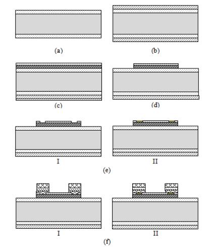
Fig. 1.
The micro-fabrication processes sequence of the metal lines
SEMICONDUCTOR TECHNOLOGY
Jie Zhang, Jianqiang Han, Yijun Yin, Lizhen Dong and Wenju Niu
Corresponding author: Jianqiang Han Email: hjqsmx@163.com
Abstract: The Ti/Pt/Au metallization system has an advantage of resisting KOH or TMAH solution etching. To form a good ohmic contact, the Ti/Pt/Au metallization system must be alloyed at 400℃. However, the process temperatures of typical MEMS packaging technologies, such as anodic bonding, glass solder bonding and eutectic bonding, generally exceed 400℃. It is puzzling if the Ti/Pt/Au system is destroyed during the subsequent packaging process. In the present work, the resistance of doped polysilicon resistors contacted by the Ti/Pt/Au metallization system that have undergone different temperatures and time are measured. The experimental results show that the ohmic contacts will be destroyed if heated to 500℃. But if a 20 nm Pt film is sputtered on heavily doped polysilicon and alloyed at 700℃ before sputtering Ti/Pt/Au films, the Pt5Si2-Ti/Pt/Au metallization system has a higher service temperature of 500℃, which exceeds process temperatures of most typical MEMS packaging technologies.
Keywords: Ti/Pt/Au metallization system, packaging, ohmic contacts, MEMS
| [1] |
Card H C. Aluminum-silicon Schottky barriers and ohmic contacts in integrated circuits. IEEE Trans Electron Devices, 1976, 23(6):538 doi: 10.1109/T-ED.1976.18449
|
| [2] |
Mayumi S, Umemoto T, Shishino M, et al. The effect of Cu addition to Al-Si interconnects on stress induced open-circuit failures. Reliab Phys Symp, 1987:15 https://www.mendeley.com/research-papers/effect-cu-addition-alsi-interconnects-stress-induced-opencircuit-failures/
|
| [3] |
Kanamori S, Sudo H. Effects of titanium layer as diffusion barrier in Ti/Pt/Au beam lead metallization on polysilicon. IEEE Trans Compon, 1982, 5(3):318 http://ieeexplore.ieee.org/document/1135973/
|
| [4] |
Sozza A, Dua C, Kerlain A, et al. Long-term reliability of Ti-Pt-Au metallization system for Schottky contact and first-level metallization on SiC MESFET. Microelectron Reliab, 2004, 44(7):1109 doi: 10.1016/j.microrel.2004.01.017
|
| [5] |
Zhou J, Xia G, Li B, et al, Structural and electrical properties of Au/Pt/Ti ohmic contacts to degenerated doped n-GaAS. Appl Phys A, 2003, 76(6):939 doi: 10.1007/s00339-002-1439-z
|
| [6] |
Wang G H, Liu Z M, Dai J L. Application of Ti-Pt-Au multi-layer metallized syetem to semiconductor devices. J Harbin Institute Technol, 1985, (4):26 http://en.cnki.com.cn/Article_en/CJFDTotal-HEBX198504004.htm
|
| [7] |
Wu Z W, Chen D Y, Xia S H. Research on the failed mechanism of anodic bonding of silicon to glass. Micronanoelectron Technol, 2010, 10:619 http://en.cnki.com.cn/Article_en/CJFDTOTAL-BDTQ201010008.htm
|
| [8] |
Xu W, Wang Y C, Luo L. Wafer-level hermetic packaging of MEMS by glass solder at low temperature. J Func Mater Devices, 2005, 11:343 http://en.cnki.com.cn/Article_en/CJFDTOTAL-GNCQ200503016.htm
|
| [9] |
Liu B W, Zhang Z H, Tan Z M, et al. Au-Si eutectic bonding technology for MEMS device. Semicond Technol, 2006, 12:896 http://en.cnki.com.cn/Article_en/CJFDTOTAL-BDTJ200612004.htm
|
| [10] |
Zhong B F. An approach to PtSi contact alloying. Microelectronics, 1988, 18:1 http://en.cnki.com.cn/Article_en/CJFDTotal-MINI198804000.htm
|
| [11] |
Xiong P, Liao S R. Study on the formation of PtSi with Pt-Si alloy. Semicond Optoelectron, 1992, 13:359 http://en.cnki.com.cn/Article_en/CJFDTotal-BDTG199204012.htm
|
| [12] |
Yin J H, Cai W, Wang M G, et al Surface and interface characteristic of sputtered nanometer PtSi film. J Semicond, 2003, 24(S1):74 http://ieeexplore.ieee.org/document/4963291/
|
| [13] |
Wang Q, Ding J N, Wang W X, et al. Fabrication of a pressure sensor gauge chip based on SIMOX. J Semicond, 2005, 26:1595 http://www.oalib.com/paper/1519655
|
| [14] |
Yin Y, Rioux R M, Erdonmez C K, et al. Formation of hollow nanocrystals through the nanoscale Kirkendall effect. Science, 2004, 304(5671):711 doi: 10.1126/science.1096566
|
| [15] |
Campbell S A. Fabrication engineering at the micro and nanoscale. 3th ed. Beijing: Publishing House of Electronics Industry, 2008
|
| [16] |
Wu D F, Yan B D. Metallurgical basis of ohmic contacts. Principle, measurement and process of ohmic contact at metal-semiconductor interface. Shanghai:Profile of Shanghai Jiao Tong University Press, 1989
|
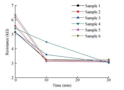
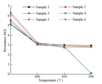
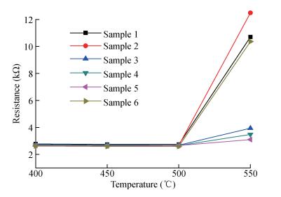
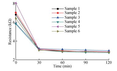
Table 1. The resistance of polysilicon resistors connected by Ti/Pt/Au system that have undergone different temperature and time
 |
Table 2.
The resistance of polysilicon resistors connected by Pt
 |
| [1] |
Card H C. Aluminum-silicon Schottky barriers and ohmic contacts in integrated circuits. IEEE Trans Electron Devices, 1976, 23(6):538 doi: 10.1109/T-ED.1976.18449
|
| [2] |
Mayumi S, Umemoto T, Shishino M, et al. The effect of Cu addition to Al-Si interconnects on stress induced open-circuit failures. Reliab Phys Symp, 1987:15 https://www.mendeley.com/research-papers/effect-cu-addition-alsi-interconnects-stress-induced-opencircuit-failures/
|
| [3] |
Kanamori S, Sudo H. Effects of titanium layer as diffusion barrier in Ti/Pt/Au beam lead metallization on polysilicon. IEEE Trans Compon, 1982, 5(3):318 http://ieeexplore.ieee.org/document/1135973/
|
| [4] |
Sozza A, Dua C, Kerlain A, et al. Long-term reliability of Ti-Pt-Au metallization system for Schottky contact and first-level metallization on SiC MESFET. Microelectron Reliab, 2004, 44(7):1109 doi: 10.1016/j.microrel.2004.01.017
|
| [5] |
Zhou J, Xia G, Li B, et al, Structural and electrical properties of Au/Pt/Ti ohmic contacts to degenerated doped n-GaAS. Appl Phys A, 2003, 76(6):939 doi: 10.1007/s00339-002-1439-z
|
| [6] |
Wang G H, Liu Z M, Dai J L. Application of Ti-Pt-Au multi-layer metallized syetem to semiconductor devices. J Harbin Institute Technol, 1985, (4):26 http://en.cnki.com.cn/Article_en/CJFDTotal-HEBX198504004.htm
|
| [7] |
Wu Z W, Chen D Y, Xia S H. Research on the failed mechanism of anodic bonding of silicon to glass. Micronanoelectron Technol, 2010, 10:619 http://en.cnki.com.cn/Article_en/CJFDTOTAL-BDTQ201010008.htm
|
| [8] |
Xu W, Wang Y C, Luo L. Wafer-level hermetic packaging of MEMS by glass solder at low temperature. J Func Mater Devices, 2005, 11:343 http://en.cnki.com.cn/Article_en/CJFDTOTAL-GNCQ200503016.htm
|
| [9] |
Liu B W, Zhang Z H, Tan Z M, et al. Au-Si eutectic bonding technology for MEMS device. Semicond Technol, 2006, 12:896 http://en.cnki.com.cn/Article_en/CJFDTOTAL-BDTJ200612004.htm
|
| [10] |
Zhong B F. An approach to PtSi contact alloying. Microelectronics, 1988, 18:1 http://en.cnki.com.cn/Article_en/CJFDTotal-MINI198804000.htm
|
| [11] |
Xiong P, Liao S R. Study on the formation of PtSi with Pt-Si alloy. Semicond Optoelectron, 1992, 13:359 http://en.cnki.com.cn/Article_en/CJFDTotal-BDTG199204012.htm
|
| [12] |
Yin J H, Cai W, Wang M G, et al Surface and interface characteristic of sputtered nanometer PtSi film. J Semicond, 2003, 24(S1):74 http://ieeexplore.ieee.org/document/4963291/
|
| [13] |
Wang Q, Ding J N, Wang W X, et al. Fabrication of a pressure sensor gauge chip based on SIMOX. J Semicond, 2005, 26:1595 http://www.oalib.com/paper/1519655
|
| [14] |
Yin Y, Rioux R M, Erdonmez C K, et al. Formation of hollow nanocrystals through the nanoscale Kirkendall effect. Science, 2004, 304(5671):711 doi: 10.1126/science.1096566
|
| [15] |
Campbell S A. Fabrication engineering at the micro and nanoscale. 3th ed. Beijing: Publishing House of Electronics Industry, 2008
|
| [16] |
Wu D F, Yan B D. Metallurgical basis of ohmic contacts. Principle, measurement and process of ohmic contact at metal-semiconductor interface. Shanghai:Profile of Shanghai Jiao Tong University Press, 1989
|


Article views: 5688 Times PDF downloads: 86 Times Cited by: 0 Times
Received: 17 January 2017 Revised: 15 February 2017 Online: Published: 01 September 2017
| Citation: |
Jie Zhang, Jianqiang Han, Yijun Yin, Lizhen Dong, Wenju Niu. Study on the failure temperature of Ti/Pt/Au and Pt5Si2-Ti/Pt/Au metallization systems[J]. Journal of Semiconductors, 2017, 38(9): 096005. doi: 10.1088/1674-4926/38/9/096005
****
J Zhang, J Q Han, Y J Yin, L Z Dong, W J Niu. Study on the failure temperature of Ti/Pt/Au and Pt5Si2-Ti/Pt/Au metallization systems[J]. J. Semicond., 2017, 38(9): 096005. doi: 10.1088/1674-4926/38/9/096005.

|
| [1] |
Card H C. Aluminum-silicon Schottky barriers and ohmic contacts in integrated circuits. IEEE Trans Electron Devices, 1976, 23(6):538 doi: 10.1109/T-ED.1976.18449
|
| [2] |
Mayumi S, Umemoto T, Shishino M, et al. The effect of Cu addition to Al-Si interconnects on stress induced open-circuit failures. Reliab Phys Symp, 1987:15 https://www.mendeley.com/research-papers/effect-cu-addition-alsi-interconnects-stress-induced-opencircuit-failures/
|
| [3] |
Kanamori S, Sudo H. Effects of titanium layer as diffusion barrier in Ti/Pt/Au beam lead metallization on polysilicon. IEEE Trans Compon, 1982, 5(3):318 http://ieeexplore.ieee.org/document/1135973/
|
| [4] |
Sozza A, Dua C, Kerlain A, et al. Long-term reliability of Ti-Pt-Au metallization system for Schottky contact and first-level metallization on SiC MESFET. Microelectron Reliab, 2004, 44(7):1109 doi: 10.1016/j.microrel.2004.01.017
|
| [5] |
Zhou J, Xia G, Li B, et al, Structural and electrical properties of Au/Pt/Ti ohmic contacts to degenerated doped n-GaAS. Appl Phys A, 2003, 76(6):939 doi: 10.1007/s00339-002-1439-z
|
| [6] |
Wang G H, Liu Z M, Dai J L. Application of Ti-Pt-Au multi-layer metallized syetem to semiconductor devices. J Harbin Institute Technol, 1985, (4):26 http://en.cnki.com.cn/Article_en/CJFDTotal-HEBX198504004.htm
|
| [7] |
Wu Z W, Chen D Y, Xia S H. Research on the failed mechanism of anodic bonding of silicon to glass. Micronanoelectron Technol, 2010, 10:619 http://en.cnki.com.cn/Article_en/CJFDTOTAL-BDTQ201010008.htm
|
| [8] |
Xu W, Wang Y C, Luo L. Wafer-level hermetic packaging of MEMS by glass solder at low temperature. J Func Mater Devices, 2005, 11:343 http://en.cnki.com.cn/Article_en/CJFDTOTAL-GNCQ200503016.htm
|
| [9] |
Liu B W, Zhang Z H, Tan Z M, et al. Au-Si eutectic bonding technology for MEMS device. Semicond Technol, 2006, 12:896 http://en.cnki.com.cn/Article_en/CJFDTOTAL-BDTJ200612004.htm
|
| [10] |
Zhong B F. An approach to PtSi contact alloying. Microelectronics, 1988, 18:1 http://en.cnki.com.cn/Article_en/CJFDTotal-MINI198804000.htm
|
| [11] |
Xiong P, Liao S R. Study on the formation of PtSi with Pt-Si alloy. Semicond Optoelectron, 1992, 13:359 http://en.cnki.com.cn/Article_en/CJFDTotal-BDTG199204012.htm
|
| [12] |
Yin J H, Cai W, Wang M G, et al Surface and interface characteristic of sputtered nanometer PtSi film. J Semicond, 2003, 24(S1):74 http://ieeexplore.ieee.org/document/4963291/
|
| [13] |
Wang Q, Ding J N, Wang W X, et al. Fabrication of a pressure sensor gauge chip based on SIMOX. J Semicond, 2005, 26:1595 http://www.oalib.com/paper/1519655
|
| [14] |
Yin Y, Rioux R M, Erdonmez C K, et al. Formation of hollow nanocrystals through the nanoscale Kirkendall effect. Science, 2004, 304(5671):711 doi: 10.1126/science.1096566
|
| [15] |
Campbell S A. Fabrication engineering at the micro and nanoscale. 3th ed. Beijing: Publishing House of Electronics Industry, 2008
|
| [16] |
Wu D F, Yan B D. Metallurgical basis of ohmic contacts. Principle, measurement and process of ohmic contact at metal-semiconductor interface. Shanghai:Profile of Shanghai Jiao Tong University Press, 1989
|

 WeChat ID
Journal of Semiconductors © 2017 All Rights Reserved 京ICP备05085259号-2

 DownLoad:

