J. Semicond. > 2018, Volume 39 > Issue 10 > 104002

SEMICONDUCTOR DEVICES

Research progress and challenges of two dimensional MoS2 field effect transistors

N Divya Bharathi and K Sivasankaran

+ Author Affiliations

 Corresponding author: K Sivasankaran, ksivasankaran@vit.ac.in, siva007i@gmail.com

DOI: 10.1088/1674-4926/39/10/104002

PDF

Turn off MathJax

Abstract: This review paper gives an outline of the recent research progress and challenges of 2D TMDs material MoS2 based device, that leads to an interesting path towards approaching the electronic applications due to its sizeable band gap. This review presents the improvement of MoS2 material as an alternate to a silicon channel in a transistor with its excellent energy band gap, thermal conductivity, and exclusive physical properties that are expected to draw attention to focusing on semiconducting devices for most futuristic applications. We discuss the band structure of MoS2 for a different number of layers with its structure, and various synthesis techniques of the MoS2 layer are also reviewed. The MoS2 based field effect transistor has attracted a great deal of attention due to its excellent properties such as mobility, on/off current ratio, and maximum on-current of the devices. The transition of mobility as a function of temperature and thickness dependence are also discussed. However, the mobility of MoS2 material is large in bulk form and lower in monolayer form. The use of a high-k gate dielectric in MoS2 FET is used to enhance the mobility of the device. Different metal contact engineering and different doping techniques were deployed to achieve low contact resistance. This review paper focuses on various aspects of layered TMDs material MoS2 based field effect transistors.

Key words: TMDs materialband structuremobilityon/off current ratiocontact resistance


[1]
Geim A K, Novoselov K S. The rise of graphene. Nat Mater, 2007, 6(3): 183 doi: 10.1038/nmat1849
[2]
Ganatra R, Zhang Q. Few-layer MoS2: a promising layered semiconductor. ACS Nano, 2014, 8(5): 4074 doi: 10.1021/nn405938z
[3]
Geim A K, Grigorieva I V. Van der Waals heterostructures. Nature, 2013, 499: 419 doi: 10.1038/nature12385
[4]
Choi M S, Qu D, Lee D, et al. Lateral MoS2 p–n junction formed by chemical doping for use in high-performance optoelectronics. ACS Nano, 2014, 8(9): 9332 doi: 10.1021/nn503284n
[5]
Izyumskaya N, Demchenko D, Avrutin V, et al. Two-dimensional MoS2 as a new material for electronic devices. Turkish J Phys, 2014, 38(3): 478
[6]
Bertolazzi S, Krasnozhon D, Kis A. Nonvolatile memory cells based on MoS2/graphene heterostructures. ACS Nano, 2013, 7(4): 3246 doi: 10.1021/nn3059136
[7]
Van Leeuwen R, Castellanos-Gomez A, Steele G A, et al. Time-domain response of atomically thin MoS2 nanomechanical resonators. Appl Phys Lett, 2014, 105(4): 041911 doi: 10.1063/1.4892072
[8]
Yin Z, Li H, Li H, et al. Single-layer MoS2 phototransistors. ACS Nano, 2012, 6(1): 74 doi: 10.1021/nn2024557
[9]
Perkins F K, Friedman A L, Cobas E, et al. Chemical vapor sensing with monolayer MoS2. Nano Lett, 2013, 13(2): 668 doi: 10.1021/nl3043079
[10]
Lopez-Sanchez O, Lembke D, Kayci M, et al. Ultrasensitive photodetectors based on monolayer MoS2. Nat Nanotechnol, 2013, 8(7): 497 doi: 10.1038/nnano.2013.100
[11]
Mak K F, Lee C, Hone J, et al. Atomically thin MoS2: a new direct-gap semiconductor. Phys Rev Lett, 2010, 105(13): 136805 doi: 10.1103/PhysRevLett.105.136805
[12]
Splendiani A, Sun L, Zhang Y, et al. Emerging photoluminescence in monolayer MoS2. Nano Lett, 2010, 10(4): 1271 doi: 10.1021/nl903868w
[13]
Ellis J K, Lucero M J, Scuseria G E. The indirect to direct band gap transition in multilayered MoS2 as predicted by screened hybrid density functional theory. Appl Phys Lett, 2011, 99(26): 261908 doi: 10.1063/1.3672219
[14]
Kang J, Cao W, Xie X, et al. Graphene and beyond-graphene 2D crystals for next-generation green electronics. Micro-and Nanotechnology Sensors, Systems, and Applications, 2014, 9083: 908305
[15]
Schwierz F, Pezoldt J, Granzner R. Two-dimensional materials and their prospects in transistor electronics. Nanoscale, 2015, 7(18): 8261 doi: 10.1039/C5NR01052G
[16]
Zhang F, Appenzeller J. Tunability of short-channel effects in MoS2 field-effect devices. Nano Lett, 2014, 15(1): 301
[17]
Ong Z Y, Fischetti M V. Mobility enhancement and temperature dependence in top-gated single-layer MoS2. Phys Rev B, 2013, 88(16): 165316 doi: 10.1103/PhysRevB.88.165316
[18]
Kim J H, Kim T H, Lee H, et al. Thickness-dependent electron mobility of single and few-layer MoS2 thin-film transistors. AIP Adv, 2016, 6(6): 065106 doi: 10.1063/1.4953809
[19]
Radisavljevic B, Kis A. Mobility engineering and a metal–insulator transition in monolayer MoS2. Nat Mater, 2013, 12(9): 815 doi: 10.1038/nmat3687
[20]
Lin M W, Kravchenko I I, Fowlkes J, et al. Thickness-dependent charge transport in few-layer MoS2 field-effect transistors. Nanotechnology, 2016, 27(16): 165203 doi: 10.1088/0957-4484/27/16/165203
[21]
Roy T, Tosun M, Cao X, et al. Dual-gated MoS2/WSe2 van der Waals tunnel diodes and transistors. ACS Nano, 2015, 9(2): 2071-9 doi: 10.1021/nn507278b
[22]
Liu L, Kumar S B, Ouyang Y, et al. Performance limits of monolayer transition metal dichalcogenide transistors. IEEE Trans Electron Devices, 2011, 58(9): 3042 doi: 10.1109/TED.2011.2159221
[23]
Kwak J Y, Hwang J, Calderon B. AIP advances electrical characteristics of multilayer MoS2 FET’s with MoS2/graphene heterojunction contacts. Nano Lett, 2014, 14(8): 4511 doi: 10.1021/nl5015316
[24]
Liu H, Neal A T, Ye P D. Channel length scaling of MoS2 MOSFETs. ACS Nano, 2012, 6(10): 8563 doi: 10.1021/nn303513c
[25]
Li X, Zhu H W. Two-dimensional MoS2: properties, preparation, and applications. J Materiom, 2015, 1(1): 33 doi: 10.1016/j.jmat.2015.03.003
[26]
Nicolosi V, Chhowalla M, Kanatzidis M G. AIP advances liquid exfoliation of layered materials. Science, 2013, 340(6139): 1226419 doi: 10.1126/science.1226419
[27]
Coleman J N, Lotya M, O’Neill A, et al. Two-dimensional nanosheets produced by liquid exfoliation of layered materials. Science, 2011, 331(6017): 568 doi: 10.1126/science.1194975
[28]
Ren J, Wang S, Cheng Z, et al. Passively Q-switched nanosecond erbium-doped fiber laser with MoS2 saturable absorber. Optics Express, 2015, 23(5): 5607 doi: 10.1364/OE.23.005607
[29]
Fominski V Yu, Nevolin V N, Romanov R I. Ion-assisted deposition of MoS2 films from laser-generated plume under pulsed electric field. J Appl Phys, 2001, 89(2): 1449 doi: 10.1063/1.1330558
[30]
Lee Y H, Zhang X Q, Zhang W, et al. Synthesis of large-area MoS2 atomic layers with chemical vapor deposition. Adv Mater, 2012, 24(17): 2320 doi: 10.1002/adma.201104798
[31]
Hong J, Hu Z, Probert M, et al. Exploring atomic defects in molybdenum disulphide monolayers. Nat Commun, 2015, 6: 6293 doi: 10.1038/ncomms7293
[32]
Li H, Kang Z, Liu Y, et al. Carbon nanodots: synthesis, properties and applications. J Mater Chem, 2012, 22(46): 24230 doi: 10.1039/c2jm34690g
[33]
Hussain S, Shehzad M A, Vikraman D, et al. Synthesis and characterization of large-area and continuous MoS2 atomic layers by RF magnetron sputtering. Nanoscale, 2016, 8(7): 4340 doi: 10.1039/C5NR09032F
[34]
Radisavljevic B, Radenovic A, Brivio J, et al. Single-layer MoS2 transistors. Nat Nanotechnol, 2011, 6(3): 147 doi: 10.1038/nnano.2010.279
[35]
Yoon Y, Ganapathi K, Salahuddin S. How good can monolayer MoS2 transistors be. Nano Lett, 2011, 11(9): 3768 doi: 10.1021/nl2018178
[36]
Liu H, Ye P D. Dual-gate MOSFET with atomic-layer-deposited Al2O3 as top gate dielectric. IEEE Electron Device Lett, 2012, 33(4): 546 doi: 10.1109/LED.2012.2184520
[37]
Yoo G, Choi S L, Lee S, et al. Enhancement-mode operation of multilayer MoS2 transistors with a fluoropolymer gate dielectric layer. Appl Phys Lett, 2016, 108(26): 263106 doi: 10.1063/1.4955024
[38]
Ganapathi K L, Bhattacharjee S, Mohan S, et al. High-performance HfO2 back gated multilayer MoS2 transistors. IEEE Electron Device Lett, 2016, 37(6): 797-800
[39]
Wen M, Xu J, Liu L, et al. Improved electrical performance of multilayer MoS2 transistor with NH3-annealed ALD HfTiO gate dielectric. IEEE Trans Electron Devices, 2017, 64(3): 1020 doi: 10.1109/TED.2017.2650920
[40]
Jena D, Konar A. Enhancement of carrier mobility in semiconductor nanostructures by dielectric engineering. Phys Rev Lett, 2007, 98(13): 136805 doi: 10.1103/PhysRevLett.98.136805
[41]
Lee C H, Vardy N, Wong W S. Multilayer MoS2 thin-film transistors employing silicon nitride and silicon oxide dielectric layers. IEEE Electron Device Lett, 2016, 37(6): 731
[42]
Qian Q, Li B, Hua M, et al. Improved gate dielectric deposition and enhanced electrical stability for single-layer MoS2 MOSFET with an AlN interfacial layer. Sci Rep, 2016, 6: 27676 doi: 10.1038/srep27676
[43]
You W X, Su P. A compact subthreshold model for short-channel monolayer transition metal dichalcogenide field-effect transistors. IEEE Trans Electron Devices, 2016, 63(7): 2971 doi: 10.1109/TED.2016.2564424
[44]
Neal A T, Liu H, Gu J J, et al. Metal contacts to MoS2: A two-dimensional semiconductor. 70th Annual Device Research Conference (DRC), 2012 : 65
[45]
Das S, Chen H Y, Penumatcha A V, et al. High performance multilayer MoS2 transistors with scandium contacts. Nano Lett, 2012, 13(1): 100
[46]
Fontana M, Deppe T, Boyd A K, et al. Electron-hole transport and photovoltaic effect in gated MoS2 Schottky junctions. Sci Rep, 2013, 3: 1634 doi: 10.1038/srep01634
[47]
Chuang S, Battaglia C, Azcatl A, et al. MoS2 p-type transistors and diodes enabled by high work function MoOx contacts. Nano Lett, 2014, 14(3): 1337 doi: 10.1021/nl4043505
[48]
Li Z, Li X, Yang J. Comparative study on electronic structures of Sc and Ti contacts with monolayer and multilayer MoS2. ACS Appl Mater Interfaces, 2015, 7(23): 12981 doi: 10.1021/acsami.5b02782
[49]
Yoon J, Park W, Bae G Y, et al. Highly flexible and transparent multilayer MoS2 transistors with graphene electrodes. Small, 2013, 9(19): 3295
[50]
Liu W, Sarkar D, Kang J, et al. Impact of contact on the operation and performance of back-gated monolayer MoS2 field-effect-transistors. ACS Nano, 2015, 9(8): 7904 doi: 10.1021/nn506512j
[51]
Kang J, Liu W, Banerjee K. High-performance MoS2 transistors with low-resistance molybdenum contacts. Appl Phys Lett, 2014, 104(9): 093106 doi: 10.1063/1.4866340
[52]
Han G, Yoon Y. Contact-dependent performance variability of monolayer MoS2 field-effect transistors. Appl Phys Lett, 2014, 105(21): 213508 doi: 10.1063/1.4902866
[53]
Chuang H J, Chamlagain B, Koehler M, et al. Low-resistance 2D/2D ohmic contacts: A universal approach to high-performance WS2, MoS2, and MoSe2 transistors. Nano Lett, 2016, 16(3): 1896 doi: 10.1021/acs.nanolett.5b05066
[54]
Yu A Y. Electron tunneling and contact resistance of metal-silicon contact barriers. Solid-State Electron, 1970, 13(2): 239 doi: 10.1016/0038-1101(70)90056-0
[55]
Du Y, Liu H, Neal A T, et al. Molecular doping of multilayer MoS2 field-effect transistors: reduction in sheet and contact resistances. IEEE Electron Device Lett, 2013, 34(10): 1328 doi: 10.1109/LED.2013.2277311
[56]
Kiriya D, Tosun M, Zhao P, et al. Air-stable surface charge transfer doping of MoS2 by benzyl viologen. J Am Chem Soc, 2014, 136(22): 7853 doi: 10.1021/ja5033327
[57]
Yang L, Majumdar K, Liu H, et al. Chloride molecular doping technique on 2D materials: WS2 and MoS2. Nano Lett, 2014, 14(11): 6275 doi: 10.1021/nl502603d
[58]
Zhang K, Feng S, Wang J, et al. Manganese doping of monolayer MoS2: the substrate is critical. Nano Lett, 2015, 15(10): 6586 doi: 10.1021/acs.nanolett.5b02315
[59]
Fang H, Tosun M, Seol G, et al. Degenerate n-doping of few-layer transition metal dichalcogenides by potassium. Nano Lett, 2013, 13(5): 1991 doi: 10.1021/nl400044m
[60]
Rastogi P, Kumar S, Bhowmick S, et al. Doping strategies for monolayer MoS2 via surface adsorption: a systematic study. J Phys Chem C, 2014, 118(51): 30309 doi: 10.1021/jp510662n
[61]
Shih C J, Wang Q H, Son Y, et al. Tuning on–off current ratio and field-effect mobility in a MoS2–graphene heterostructure via Schottky barrier modulation. ACS Nano, 2014, 19; 8(6): 5790
[62]
Du Y, Yang L, Zhang J, et al. MoS2 Field-effect transistors with graphene/metal heterocontacts. IEEE Electron Device Lett, 2014, 35(5): 599 doi: 10.1109/LED.2014.2313340
[63]
Zou X, Wang J, Chiu C H, et al. Interface engineering for high-performance top-gated MoS2 field-effect transistors. Adv Mater, 2014, 26(36): 6255 doi: 10.1002/adma.201402008
[64]
Zou X, Huang C W, Wang L, et al. Dielectric engineering of a boron nitride/hafnium oxide heterostructure for high-performance 2D field effect transistors. Adv Mater, 2016, 28(10): 2062 doi: 10.1002/adma.201505205
[65]
Georgiou T, Jalil R, Belle B D, et al. Vertical field-effect transistor based on graphene–WS2 heterostructures for flexible and transparent electronics. Nat Nanotechnol, 2013, 8(2): 100 doi: 10.1038/nnano.2012.224
[66]
Schwarz S, Dufferwiel S, Walker P M, et al. Two-dimensional metal–chalcogenide films in tunable optical microcavities. Nano Lett, 2014, 14(12): 7003 doi: 10.1021/nl503312x
[67]
Traversi F, Russo V, Sordan R. Integrated complementary graphene inverter. Appl Phys Lett, 2009, 94(22): 150
[68]
Radisavljevic B, Whitwick M B, Kis A. Integrated circuits and logic operations based on single-layer MoS2. ACS Nano, 2011, 5(12): 9934 doi: 10.1021/nn203715c
[69]
Radisavljevic B, Whitwick M B, Kis A. Small-signal amplifier based on single-layer MoS2. Appl Phys Lett, 2012, 101(4): 043103 doi: 10.1063/1.4738986
[70]
Wang H, Yu L, Lee Y H, et al. Integrated circuits based on bilayer MoS2 transistors. Nano Lett, 2012, 12(9): 4674 doi: 10.1021/nl302015v
[71]
Kim S, Konar A, Hwang W S, et al. High-mobility and low-power thin-film transistors based on multilayer MoS2 crystals. Nat Commun, 2012, 3: 2018
[72]
Wang X R, Shi Y, Zhang R. Field-effect transistors based on two-dimensional materials for logic applications. Chin Phys B, 2013, 22(9): 098505 doi: 10.1088/1674-1056/22/9/098505
[73]
Wu D, Zhang Z, Lv D, et al. High mobility top gated field-effect transistors and integrated circuits based on chemical vapor deposition-derived monolayer MoS2. Mater Express, 2016, 6(2): 198 doi: 10.1166/mex.2016.1289
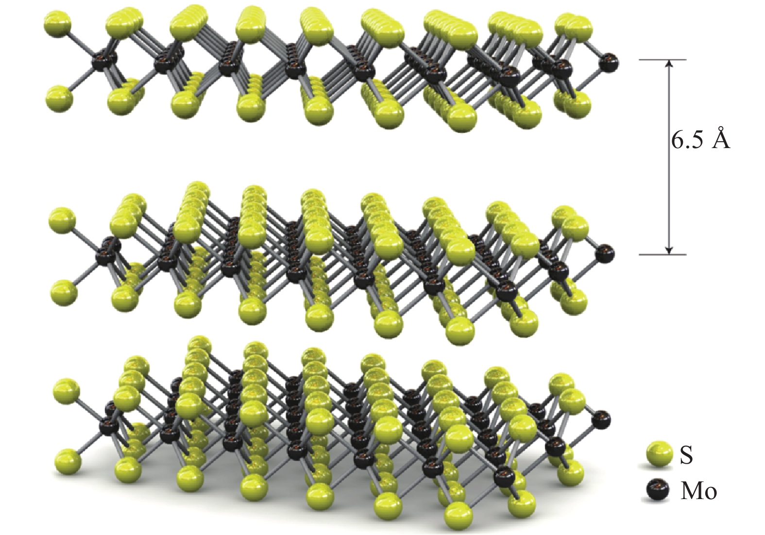
Fig. 1.  (Color online) Schematic structure of MoS2 layer[31].

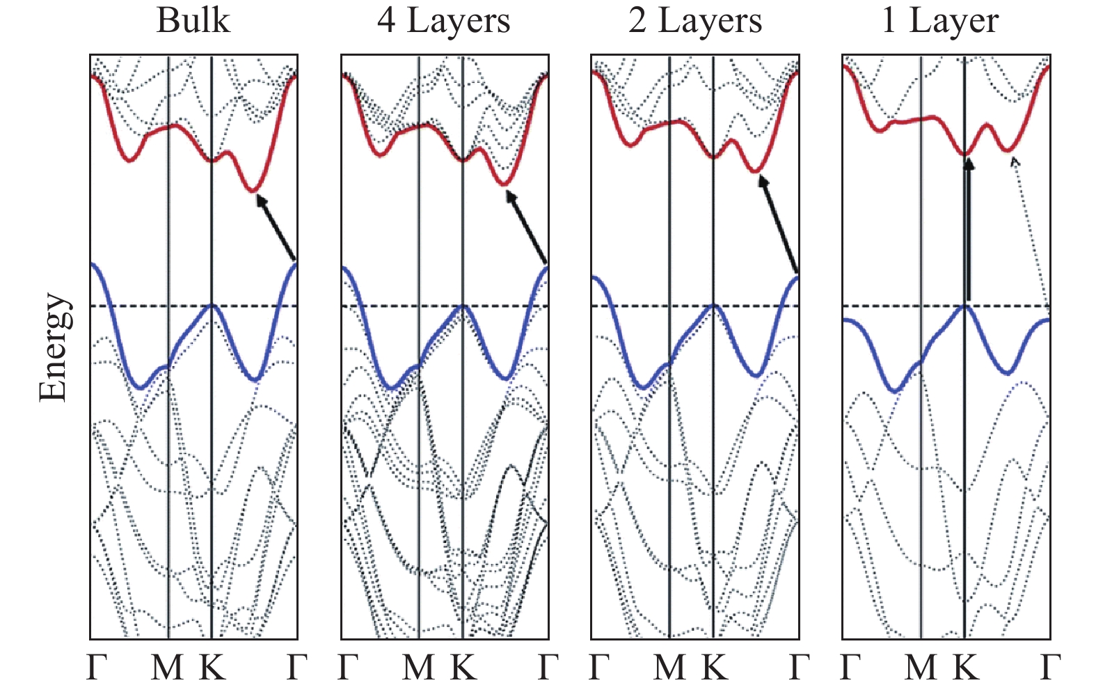
Fig. 2.  (Color online) Band structure for different MoS2 layers[13].

Fig. 3.  (Color online) Scenario of channel material for logic MOSFET[15].

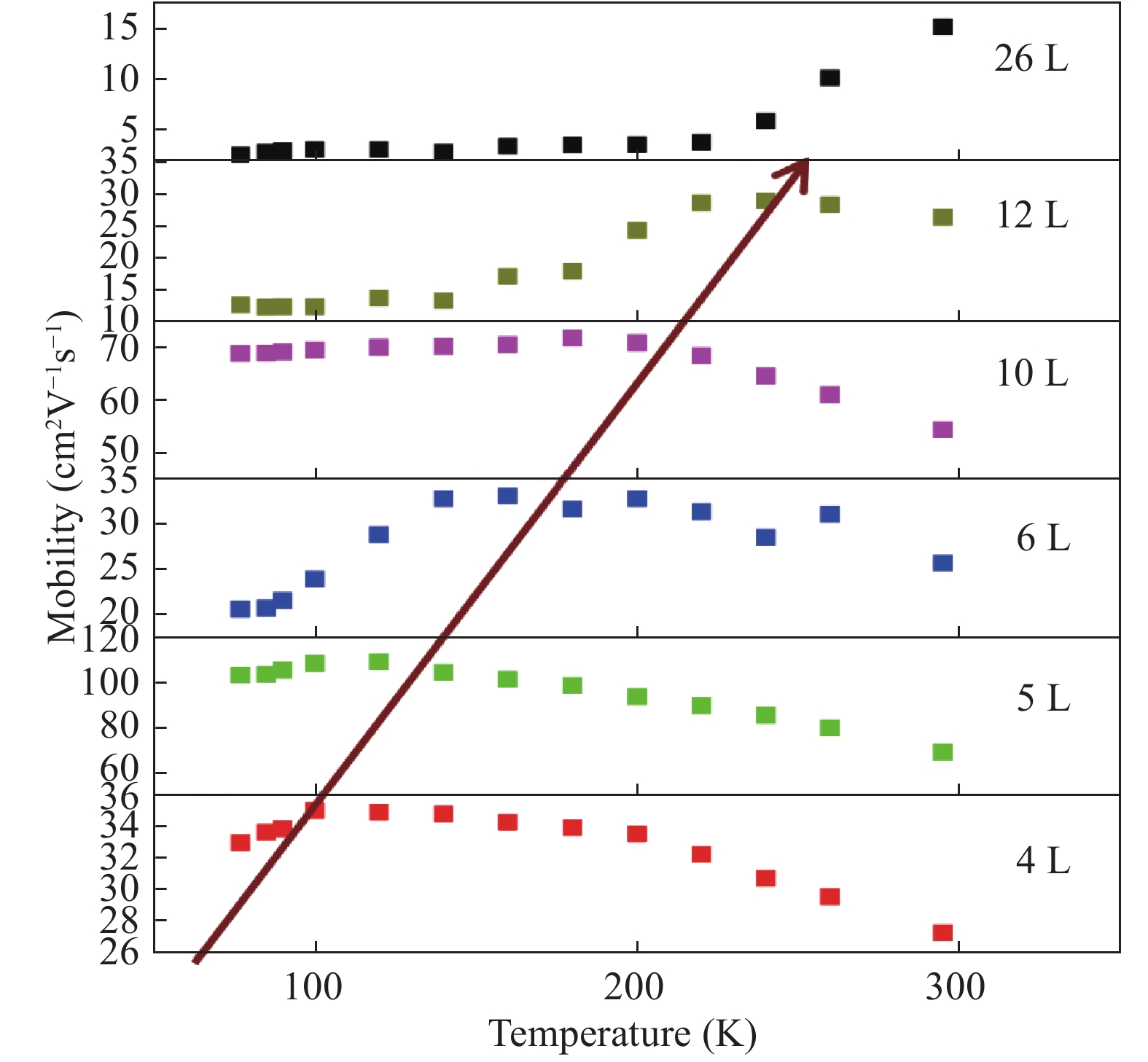
Fig. 4.  (Color online) Mobility and temperature for different channel layers/thickness[17].

Fig. 5.  (Color online) Synthesizing monolayer MoS2 from bulk crystal using the scotch tape method.

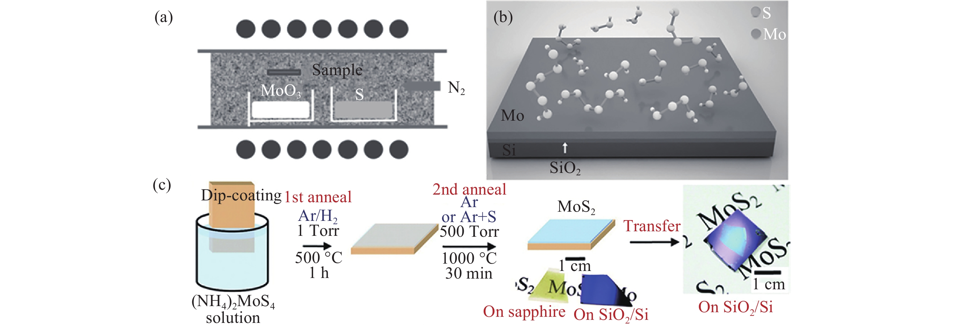
Fig. 6.  (Color online) CVD experimental set-up. (a) Sulfurization of MoO3 powder. (b) Sulfurization of Mo films. (c) Schematic illustration of the two-step thermal decomposition of (NH4)2MoS4[30].

Fig. 7.  (Color online) Single-layer MoS2 transistor[34].

Fig. 8.  (Color online) IDSVGS characteristics for different dielectric materials[43].

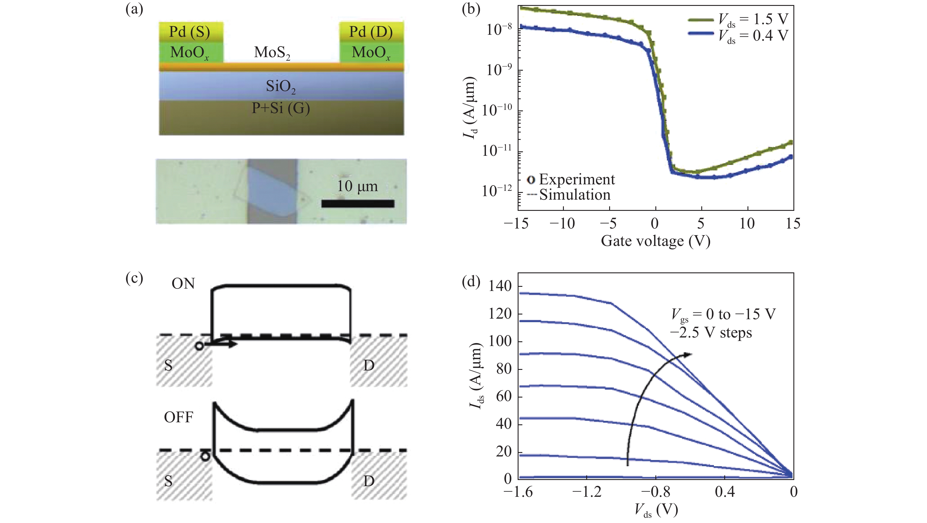
Fig. 9.  (Color online) (a) Schematic and optical microscope image. (b) IDSVGS characteristics at different drain voltage. (c) Band diagram with ON and OFF states. (d) IDSVDS characteristics with MoOx contact at VGS varies from 0 to –15 V[47].

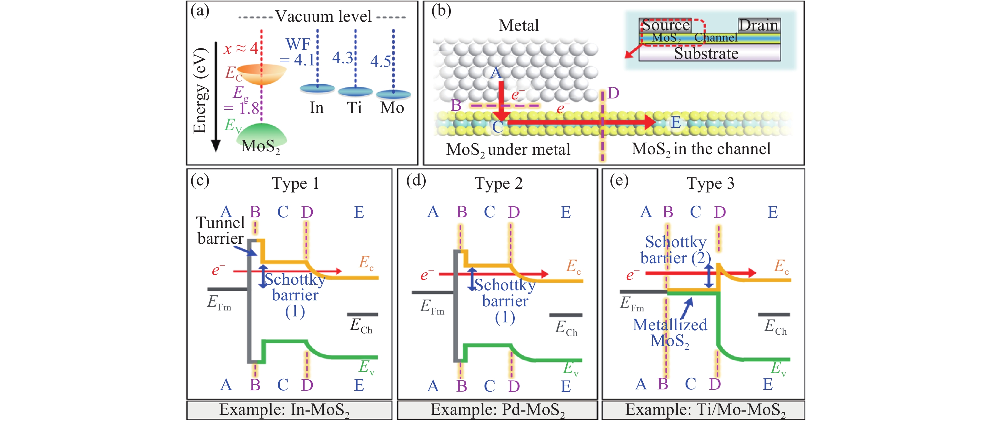
Fig. 11.  (Color online) Band alignment and band diagram of MoS2 with different metal contacts[51].

Fig. 10.  (Color online) IDVG characteristics for multilayer MoS2 transistor for different contact metals[48].

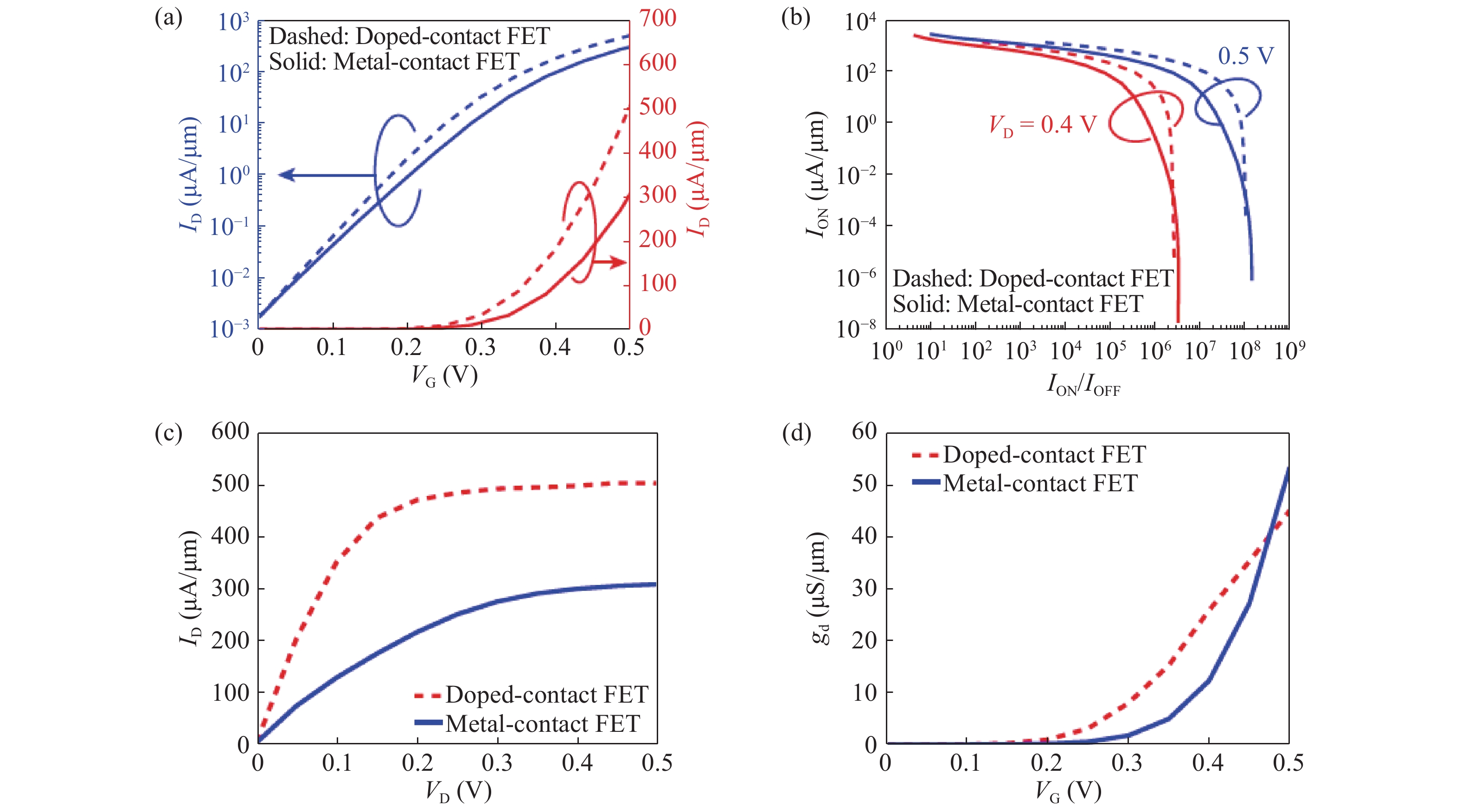
Fig. 12.  (Color online) (a) IDVG characteristics. (b) Ion and Ion/Ioff ratio. (c) IDVD characteristics. (d) Output conductance[52].

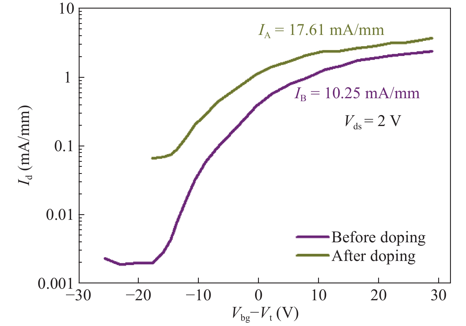
Fig. 13.  (Color online) Electrical behavior of MoS2 FET before and after PEI doping[55].

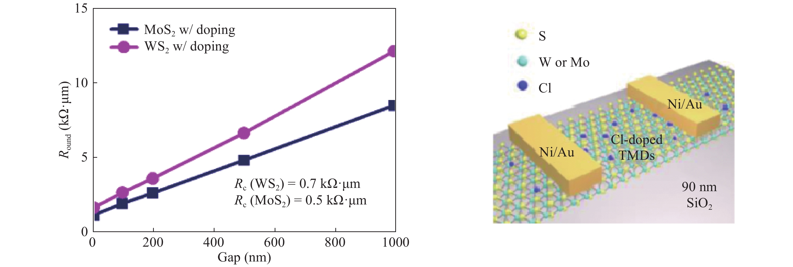
Fig. 14.  (Color online) Chlorine doped TMDs FET and contact resistance after doping for MoS2/WS2[57].

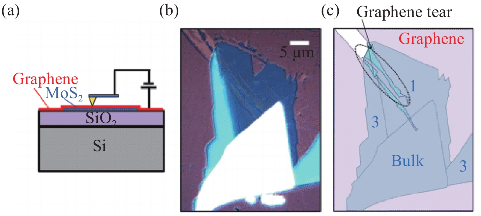
Fig. 15.  (Color online) (a) Cross-sectional view of graphene/MoS2 heterostructure. (b) Optical microscope image. (c) Topographical diagram for a CVD graphene-coated MoS2 single crystal[61].

Fig. 16.  (Color online) (a) Output characteristic with and without graphene at Vbg from −20 to 5 V. (b) Transfer curve of hetero-contacts for FET in linear (right) and log (left) scale[62].

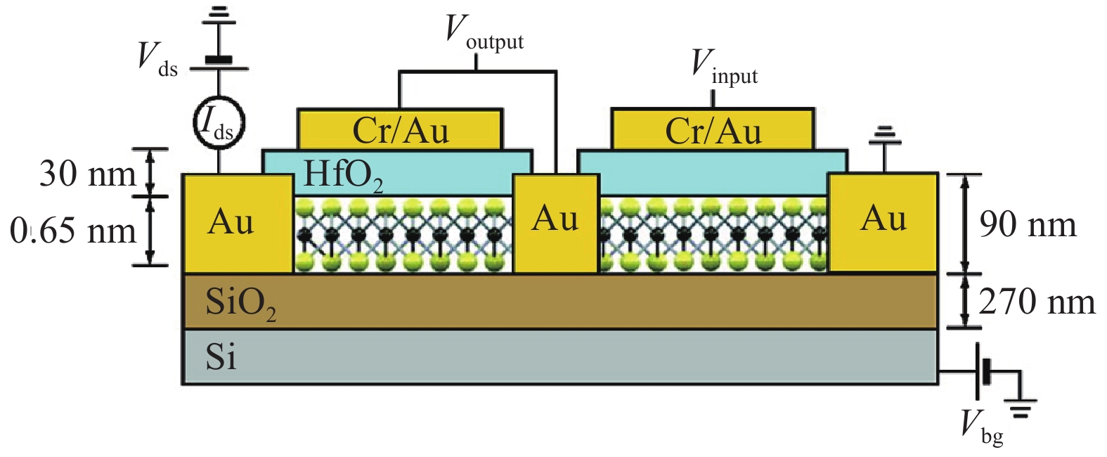
Fig. 17.  (Color online) Single layer of integrated MoS2 transistor[68].

Fig. 18.  (Color online) (a) Optical micrograph of the NAND gate and the SRAM fabricated on the same bilayer MoS2 thin film. (b) The output voltage of the flip-flop memory cell. (c) Output voltage for NAND gate[71].

Table 1.   Performance summary of MoS2 transistor.

Type of layer Ion SS (mV/dec) Mobility (cm2/(V·s)) Ion/Ioff Ref.
SL 2.5 μA/μm 74 217 108 [34]
SL 1.6 mA/μm 60 200 1010 [35]
ML 7.07 mA/mm 140 517 108 [36]
ML 180 μA/μm 100–110 11 106 [38]
ML 461 nA/μm 100 31.1 106 [39]
ML 1 μA/μm 74 700 106 [45]
SL 1L = 18 μA/μm 1L = 11 105 [51]
ML 5L = 34 μA/μm 5L = 25 106 [51]
SL 300 μA/μm 65 106 [52]
ML 160 mA/mm 50.4 107 [62]
SL 1.5 μA/μm 200 36.4 106 [73]
*SL: single layer; ML: multilayer.
DownLoad: CSV
[1]
Geim A K, Novoselov K S. The rise of graphene. Nat Mater, 2007, 6(3): 183 doi: 10.1038/nmat1849
[2]
Ganatra R, Zhang Q. Few-layer MoS2: a promising layered semiconductor. ACS Nano, 2014, 8(5): 4074 doi: 10.1021/nn405938z
[3]
Geim A K, Grigorieva I V. Van der Waals heterostructures. Nature, 2013, 499: 419 doi: 10.1038/nature12385
[4]
Choi M S, Qu D, Lee D, et al. Lateral MoS2 p–n junction formed by chemical doping for use in high-performance optoelectronics. ACS Nano, 2014, 8(9): 9332 doi: 10.1021/nn503284n
[5]
Izyumskaya N, Demchenko D, Avrutin V, et al. Two-dimensional MoS2 as a new material for electronic devices. Turkish J Phys, 2014, 38(3): 478
[6]
Bertolazzi S, Krasnozhon D, Kis A. Nonvolatile memory cells based on MoS2/graphene heterostructures. ACS Nano, 2013, 7(4): 3246 doi: 10.1021/nn3059136
[7]
Van Leeuwen R, Castellanos-Gomez A, Steele G A, et al. Time-domain response of atomically thin MoS2 nanomechanical resonators. Appl Phys Lett, 2014, 105(4): 041911 doi: 10.1063/1.4892072
[8]
Yin Z, Li H, Li H, et al. Single-layer MoS2 phototransistors. ACS Nano, 2012, 6(1): 74 doi: 10.1021/nn2024557
[9]
Perkins F K, Friedman A L, Cobas E, et al. Chemical vapor sensing with monolayer MoS2. Nano Lett, 2013, 13(2): 668 doi: 10.1021/nl3043079
[10]
Lopez-Sanchez O, Lembke D, Kayci M, et al. Ultrasensitive photodetectors based on monolayer MoS2. Nat Nanotechnol, 2013, 8(7): 497 doi: 10.1038/nnano.2013.100
[11]
Mak K F, Lee C, Hone J, et al. Atomically thin MoS2: a new direct-gap semiconductor. Phys Rev Lett, 2010, 105(13): 136805 doi: 10.1103/PhysRevLett.105.136805
[12]
Splendiani A, Sun L, Zhang Y, et al. Emerging photoluminescence in monolayer MoS2. Nano Lett, 2010, 10(4): 1271 doi: 10.1021/nl903868w
[13]
Ellis J K, Lucero M J, Scuseria G E. The indirect to direct band gap transition in multilayered MoS2 as predicted by screened hybrid density functional theory. Appl Phys Lett, 2011, 99(26): 261908 doi: 10.1063/1.3672219
[14]
Kang J, Cao W, Xie X, et al. Graphene and beyond-graphene 2D crystals for next-generation green electronics. Micro-and Nanotechnology Sensors, Systems, and Applications, 2014, 9083: 908305
[15]
Schwierz F, Pezoldt J, Granzner R. Two-dimensional materials and their prospects in transistor electronics. Nanoscale, 2015, 7(18): 8261 doi: 10.1039/C5NR01052G
[16]
Zhang F, Appenzeller J. Tunability of short-channel effects in MoS2 field-effect devices. Nano Lett, 2014, 15(1): 301
[17]
Ong Z Y, Fischetti M V. Mobility enhancement and temperature dependence in top-gated single-layer MoS2. Phys Rev B, 2013, 88(16): 165316 doi: 10.1103/PhysRevB.88.165316
[18]
Kim J H, Kim T H, Lee H, et al. Thickness-dependent electron mobility of single and few-layer MoS2 thin-film transistors. AIP Adv, 2016, 6(6): 065106 doi: 10.1063/1.4953809
[19]
Radisavljevic B, Kis A. Mobility engineering and a metal–insulator transition in monolayer MoS2. Nat Mater, 2013, 12(9): 815 doi: 10.1038/nmat3687
[20]
Lin M W, Kravchenko I I, Fowlkes J, et al. Thickness-dependent charge transport in few-layer MoS2 field-effect transistors. Nanotechnology, 2016, 27(16): 165203 doi: 10.1088/0957-4484/27/16/165203
[21]
Roy T, Tosun M, Cao X, et al. Dual-gated MoS2/WSe2 van der Waals tunnel diodes and transistors. ACS Nano, 2015, 9(2): 2071-9 doi: 10.1021/nn507278b
[22]
Liu L, Kumar S B, Ouyang Y, et al. Performance limits of monolayer transition metal dichalcogenide transistors. IEEE Trans Electron Devices, 2011, 58(9): 3042 doi: 10.1109/TED.2011.2159221
[23]
Kwak J Y, Hwang J, Calderon B. AIP advances electrical characteristics of multilayer MoS2 FET’s with MoS2/graphene heterojunction contacts. Nano Lett, 2014, 14(8): 4511 doi: 10.1021/nl5015316
[24]
Liu H, Neal A T, Ye P D. Channel length scaling of MoS2 MOSFETs. ACS Nano, 2012, 6(10): 8563 doi: 10.1021/nn303513c
[25]
Li X, Zhu H W. Two-dimensional MoS2: properties, preparation, and applications. J Materiom, 2015, 1(1): 33 doi: 10.1016/j.jmat.2015.03.003
[26]
Nicolosi V, Chhowalla M, Kanatzidis M G. AIP advances liquid exfoliation of layered materials. Science, 2013, 340(6139): 1226419 doi: 10.1126/science.1226419
[27]
Coleman J N, Lotya M, O’Neill A, et al. Two-dimensional nanosheets produced by liquid exfoliation of layered materials. Science, 2011, 331(6017): 568 doi: 10.1126/science.1194975
[28]
Ren J, Wang S, Cheng Z, et al. Passively Q-switched nanosecond erbium-doped fiber laser with MoS2 saturable absorber. Optics Express, 2015, 23(5): 5607 doi: 10.1364/OE.23.005607
[29]
Fominski V Yu, Nevolin V N, Romanov R I. Ion-assisted deposition of MoS2 films from laser-generated plume under pulsed electric field. J Appl Phys, 2001, 89(2): 1449 doi: 10.1063/1.1330558
[30]
Lee Y H, Zhang X Q, Zhang W, et al. Synthesis of large-area MoS2 atomic layers with chemical vapor deposition. Adv Mater, 2012, 24(17): 2320 doi: 10.1002/adma.201104798
[31]
Hong J, Hu Z, Probert M, et al. Exploring atomic defects in molybdenum disulphide monolayers. Nat Commun, 2015, 6: 6293 doi: 10.1038/ncomms7293
[32]
Li H, Kang Z, Liu Y, et al. Carbon nanodots: synthesis, properties and applications. J Mater Chem, 2012, 22(46): 24230 doi: 10.1039/c2jm34690g
[33]
Hussain S, Shehzad M A, Vikraman D, et al. Synthesis and characterization of large-area and continuous MoS2 atomic layers by RF magnetron sputtering. Nanoscale, 2016, 8(7): 4340 doi: 10.1039/C5NR09032F
[34]
Radisavljevic B, Radenovic A, Brivio J, et al. Single-layer MoS2 transistors. Nat Nanotechnol, 2011, 6(3): 147 doi: 10.1038/nnano.2010.279
[35]
Yoon Y, Ganapathi K, Salahuddin S. How good can monolayer MoS2 transistors be. Nano Lett, 2011, 11(9): 3768 doi: 10.1021/nl2018178
[36]
Liu H, Ye P D. Dual-gate MOSFET with atomic-layer-deposited Al2O3 as top gate dielectric. IEEE Electron Device Lett, 2012, 33(4): 546 doi: 10.1109/LED.2012.2184520
[37]
Yoo G, Choi S L, Lee S, et al. Enhancement-mode operation of multilayer MoS2 transistors with a fluoropolymer gate dielectric layer. Appl Phys Lett, 2016, 108(26): 263106 doi: 10.1063/1.4955024
[38]
Ganapathi K L, Bhattacharjee S, Mohan S, et al. High-performance HfO2 back gated multilayer MoS2 transistors. IEEE Electron Device Lett, 2016, 37(6): 797-800
[39]
Wen M, Xu J, Liu L, et al. Improved electrical performance of multilayer MoS2 transistor with NH3-annealed ALD HfTiO gate dielectric. IEEE Trans Electron Devices, 2017, 64(3): 1020 doi: 10.1109/TED.2017.2650920
[40]
Jena D, Konar A. Enhancement of carrier mobility in semiconductor nanostructures by dielectric engineering. Phys Rev Lett, 2007, 98(13): 136805 doi: 10.1103/PhysRevLett.98.136805
[41]
Lee C H, Vardy N, Wong W S. Multilayer MoS2 thin-film transistors employing silicon nitride and silicon oxide dielectric layers. IEEE Electron Device Lett, 2016, 37(6): 731
[42]
Qian Q, Li B, Hua M, et al. Improved gate dielectric deposition and enhanced electrical stability for single-layer MoS2 MOSFET with an AlN interfacial layer. Sci Rep, 2016, 6: 27676 doi: 10.1038/srep27676
[43]
You W X, Su P. A compact subthreshold model for short-channel monolayer transition metal dichalcogenide field-effect transistors. IEEE Trans Electron Devices, 2016, 63(7): 2971 doi: 10.1109/TED.2016.2564424
[44]
Neal A T, Liu H, Gu J J, et al. Metal contacts to MoS2: A two-dimensional semiconductor. 70th Annual Device Research Conference (DRC), 2012 : 65
[45]
Das S, Chen H Y, Penumatcha A V, et al. High performance multilayer MoS2 transistors with scandium contacts. Nano Lett, 2012, 13(1): 100
[46]
Fontana M, Deppe T, Boyd A K, et al. Electron-hole transport and photovoltaic effect in gated MoS2 Schottky junctions. Sci Rep, 2013, 3: 1634 doi: 10.1038/srep01634
[47]
Chuang S, Battaglia C, Azcatl A, et al. MoS2 p-type transistors and diodes enabled by high work function MoOx contacts. Nano Lett, 2014, 14(3): 1337 doi: 10.1021/nl4043505
[48]
Li Z, Li X, Yang J. Comparative study on electronic structures of Sc and Ti contacts with monolayer and multilayer MoS2. ACS Appl Mater Interfaces, 2015, 7(23): 12981 doi: 10.1021/acsami.5b02782
[49]
Yoon J, Park W, Bae G Y, et al. Highly flexible and transparent multilayer MoS2 transistors with graphene electrodes. Small, 2013, 9(19): 3295
[50]
Liu W, Sarkar D, Kang J, et al. Impact of contact on the operation and performance of back-gated monolayer MoS2 field-effect-transistors. ACS Nano, 2015, 9(8): 7904 doi: 10.1021/nn506512j
[51]
Kang J, Liu W, Banerjee K. High-performance MoS2 transistors with low-resistance molybdenum contacts. Appl Phys Lett, 2014, 104(9): 093106 doi: 10.1063/1.4866340
[52]
Han G, Yoon Y. Contact-dependent performance variability of monolayer MoS2 field-effect transistors. Appl Phys Lett, 2014, 105(21): 213508 doi: 10.1063/1.4902866
[53]
Chuang H J, Chamlagain B, Koehler M, et al. Low-resistance 2D/2D ohmic contacts: A universal approach to high-performance WS2, MoS2, and MoSe2 transistors. Nano Lett, 2016, 16(3): 1896 doi: 10.1021/acs.nanolett.5b05066
[54]
Yu A Y. Electron tunneling and contact resistance of metal-silicon contact barriers. Solid-State Electron, 1970, 13(2): 239 doi: 10.1016/0038-1101(70)90056-0
[55]
Du Y, Liu H, Neal A T, et al. Molecular doping of multilayer MoS2 field-effect transistors: reduction in sheet and contact resistances. IEEE Electron Device Lett, 2013, 34(10): 1328 doi: 10.1109/LED.2013.2277311
[56]
Kiriya D, Tosun M, Zhao P, et al. Air-stable surface charge transfer doping of MoS2 by benzyl viologen. J Am Chem Soc, 2014, 136(22): 7853 doi: 10.1021/ja5033327
[57]
Yang L, Majumdar K, Liu H, et al. Chloride molecular doping technique on 2D materials: WS2 and MoS2. Nano Lett, 2014, 14(11): 6275 doi: 10.1021/nl502603d
[58]
Zhang K, Feng S, Wang J, et al. Manganese doping of monolayer MoS2: the substrate is critical. Nano Lett, 2015, 15(10): 6586 doi: 10.1021/acs.nanolett.5b02315
[59]
Fang H, Tosun M, Seol G, et al. Degenerate n-doping of few-layer transition metal dichalcogenides by potassium. Nano Lett, 2013, 13(5): 1991 doi: 10.1021/nl400044m
[60]
Rastogi P, Kumar S, Bhowmick S, et al. Doping strategies for monolayer MoS2 via surface adsorption: a systematic study. J Phys Chem C, 2014, 118(51): 30309 doi: 10.1021/jp510662n
[61]
Shih C J, Wang Q H, Son Y, et al. Tuning on–off current ratio and field-effect mobility in a MoS2–graphene heterostructure via Schottky barrier modulation. ACS Nano, 2014, 19; 8(6): 5790
[62]
Du Y, Yang L, Zhang J, et al. MoS2 Field-effect transistors with graphene/metal heterocontacts. IEEE Electron Device Lett, 2014, 35(5): 599 doi: 10.1109/LED.2014.2313340
[63]
Zou X, Wang J, Chiu C H, et al. Interface engineering for high-performance top-gated MoS2 field-effect transistors. Adv Mater, 2014, 26(36): 6255 doi: 10.1002/adma.201402008
[64]
Zou X, Huang C W, Wang L, et al. Dielectric engineering of a boron nitride/hafnium oxide heterostructure for high-performance 2D field effect transistors. Adv Mater, 2016, 28(10): 2062 doi: 10.1002/adma.201505205
[65]
Georgiou T, Jalil R, Belle B D, et al. Vertical field-effect transistor based on graphene–WS2 heterostructures for flexible and transparent electronics. Nat Nanotechnol, 2013, 8(2): 100 doi: 10.1038/nnano.2012.224
[66]
Schwarz S, Dufferwiel S, Walker P M, et al. Two-dimensional metal–chalcogenide films in tunable optical microcavities. Nano Lett, 2014, 14(12): 7003 doi: 10.1021/nl503312x
[67]
Traversi F, Russo V, Sordan R. Integrated complementary graphene inverter. Appl Phys Lett, 2009, 94(22): 150
[68]
Radisavljevic B, Whitwick M B, Kis A. Integrated circuits and logic operations based on single-layer MoS2. ACS Nano, 2011, 5(12): 9934 doi: 10.1021/nn203715c
[69]
Radisavljevic B, Whitwick M B, Kis A. Small-signal amplifier based on single-layer MoS2. Appl Phys Lett, 2012, 101(4): 043103 doi: 10.1063/1.4738986
[70]
Wang H, Yu L, Lee Y H, et al. Integrated circuits based on bilayer MoS2 transistors. Nano Lett, 2012, 12(9): 4674 doi: 10.1021/nl302015v
[71]
Kim S, Konar A, Hwang W S, et al. High-mobility and low-power thin-film transistors based on multilayer MoS2 crystals. Nat Commun, 2012, 3: 2018
[72]
Wang X R, Shi Y, Zhang R. Field-effect transistors based on two-dimensional materials for logic applications. Chin Phys B, 2013, 22(9): 098505 doi: 10.1088/1674-1056/22/9/098505
[73]
Wu D, Zhang Z, Lv D, et al. High mobility top gated field-effect transistors and integrated circuits based on chemical vapor deposition-derived monolayer MoS2. Mater Express, 2016, 6(2): 198 doi: 10.1166/mex.2016.1289
  • Search

    Advanced Search >>

    GET CITATION

    shu

    Export: BibTex EndNote

    Article Metrics

    Article views: 6020 Times PDF downloads: 355 Times Cited by: 0 Times

    History

    Received: 20 February 2018 Revised: 11 April 2018 Online: Uncorrected proof: 25 May 2018Published: 09 October 2018

    Catalog

      Email This Article

      User name:
      Email:*请输入正确邮箱
      Code:*验证码错误
      N Divya Bharathi, K Sivasankaran. Research progress and challenges of two dimensional MoS2 field effect transistors[J]. Journal of Semiconductors, 2018, 39(10): 104002. doi: 10.1088/1674-4926/39/10/104002 ****N D Bharathi, K Sivasankaran, Research progress and challenges of two dimensional MoS2 field effect transistors[J]. J. Semicond., 2018, 39(10): 104002. doi: 10.1088/1674-4926/39/10/104002.
      Citation:
      N Divya Bharathi, K Sivasankaran. Research progress and challenges of two dimensional MoS2 field effect transistors[J]. Journal of Semiconductors, 2018, 39(10): 104002. doi: 10.1088/1674-4926/39/10/104002 ****
      N D Bharathi, K Sivasankaran, Research progress and challenges of two dimensional MoS2 field effect transistors[J]. J. Semicond., 2018, 39(10): 104002. doi: 10.1088/1674-4926/39/10/104002.

      Research progress and challenges of two dimensional MoS2 field effect transistors

      DOI: 10.1088/1674-4926/39/10/104002
      More Information
      • Corresponding author: ksivasankaran@vit.ac.in, siva007i@gmail.com
      • Received Date: 2018-02-20
      • Revised Date: 2018-04-11
      • Published Date: 2018-10-01

      Catalog

        /

        DownLoad:  Full-Size Img  PowerPoint
        Return
        Return