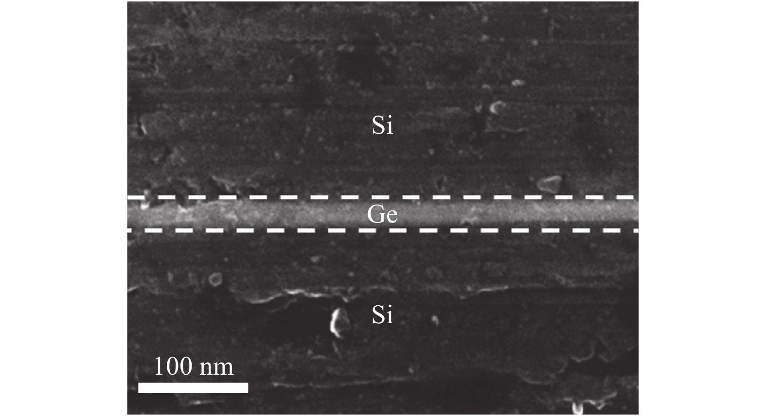
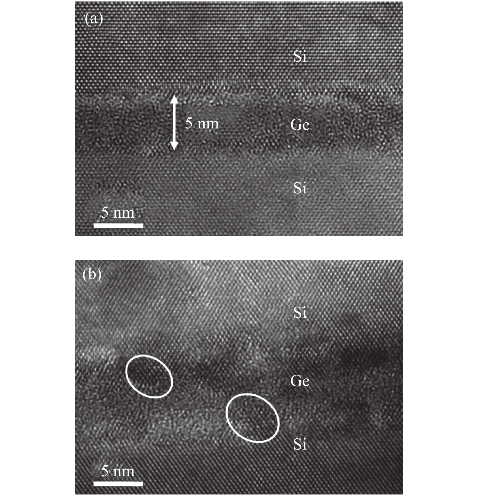
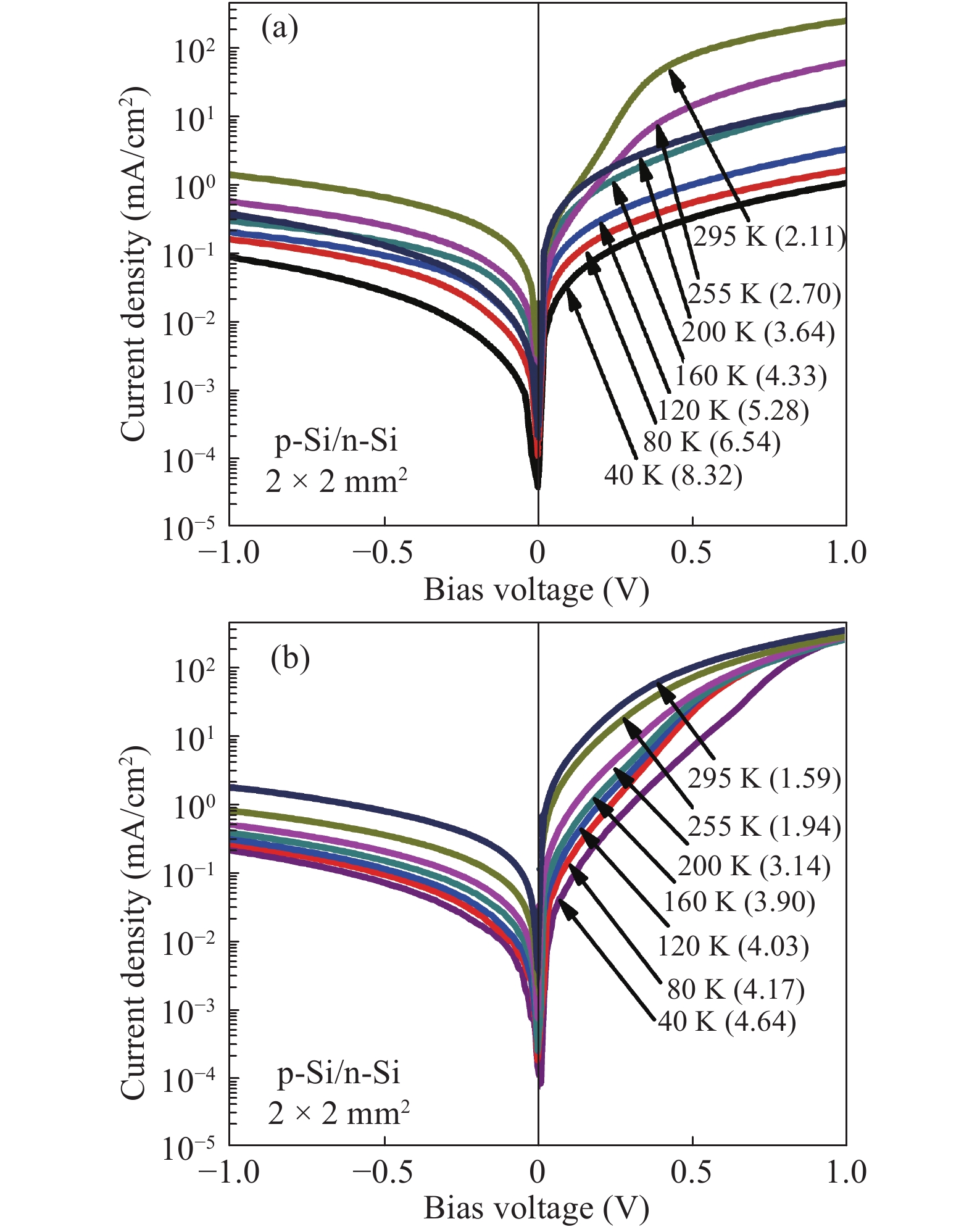
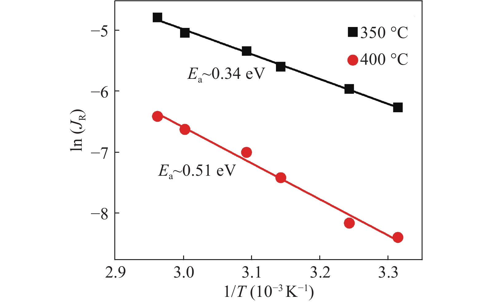
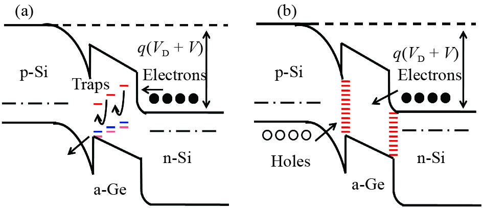
J. Semicond. > 2018, Volume 39 > Issue 11 > 113001

SEMICONDUCTOR MATERIALS

Electrical properties of Si/Si bonded wafers based on an amorphous Ge interlayer

Shaoming Lin, Shaoying Ke, Yujie Ye, Donglin Huang, Jinyong Wu, Songyan Chen, Cheng Li, Jianyuan Wang and Wei Huang

+ Author Affiliations

 Corresponding author: Songyan Chen, Email: sychen@xmu.edu.cn

DOI: 10.1088/1674-4926/39/11/113001

PDF

Turn off MathJax

Abstract: An amorphous Ge (a-Ge) intermediate layer is introduced into the Si bonded interface to lower the annealing temperature and achieve good electrical characteristics. The interface and electrical characteristics of n-Si/n-Si and p-Si/n-Si junctions manufactured by low-temperature wafer bonding based on a thin amorphous Ge are investigated. It is found that the bubble density tremendously decreases when the a-Ge film is not immersed in DI water. This is due to the decrease of the –OH groups. In addition, when the samples are annealed at 400 °C for 20 h, the bubbles totally disappear. This can be explained by the appearance of the polycrystalline Ge (absorption of H2) at the bonded interface. The junction resistance of the n-Si/n-Si bonded wafers decreases with the increase of the annealing temperature. This is consistent with the recrystallization of the a-Ge when high-temperature annealing is conducted. The carrier transport of the Si-based PN junction annealed at 350 °C is consistent with the trap-assisted tunneling model and that annealed at 400 °C is related to the carrier recombination model.

Key words: carrier transportamorphous Ge interlayerbubble-free interfaceelectrical characteristics

The wafer bonding technique, in which semiconductor junctions with different crystal structures or lattice constants can be formed by using this method, is playing an important role in micro electromechanical systems (MEMS)[1, 2], photoelectric devices[3, 4], and high-performance silicon-on-insulator (SOI) wafers[5, 6]. At present, many methods, such as conventional hydrophilic bonding, HF-treated hydrophobic bonding, surface-activated bonding (SAB), and plasma-assisted bonding, have been applied to form Si-based junctions.

Compared to conventional hydrophobic and hydrophilic wafer bonding, the plasma-assisted method can achieve a strong bonding strength at low temperature. Nevertheless, because of the hydrophilic reaction during post annealing, an oxidation layer was formed at the bonded interface[7]. The existence of the oxidation layer greatly limits the carrier transport across the bonded interface. It was reported that the I–V curves of the p-Si/p-Si junctions based on the plasma treatment technique shows nonlinear characteristics, and large resistance exists at the bonded interface by reason of the fact that the oxide interlayer is regarded as a potential barrier at the bonded interface[8]. The junction resistance of the bonded wafers based on the traditional hydrophilic methods is also at least three orders of magnitude larger than that of the bare Si substrate[9].

Refs. [10, 11] reported that the linear I–V characteristic of the Si bonded wafers can be achieved by a high-vacuum activation method[10] or hydrophobic bonding[11]. The high-vacuum activation method can form an oxide-free bonded interface after the surface has been cleaned by Ar+ bombardment and wafer bonding in a high vacuum. However, an amorphous-like layer appears around the bonded interface and is recrystallized after thermal annealing at 600 °C[12]. In addition, the cost of the ultra-high vacuum cannot be ignored.

The hydrophobic direct bonding can also produce an oxide-free bonded interface due to the fact that the hydrophobic reaction cannot produce the oxide interlayer at the Si/Si interface[11]. It is reported that the ohmic Si/Si junctions[13] and semi-ohmic p+-Si/n+-Si reverse biased tunnel diodes[14, 15] have been fabricated by the hydrophobic method. Unfortunately, this hydrophobic direct bonding is difficult to achieve due to the fact that the Si–H bond is weaker than the Si–OH bond. Similarly, in order to improve the bonding strength and the electrical characteristics of bonded wafer pairs, high-temperature post annealing is inevitable.

In this work, an amorphous Ge intermediate layer is introduced into the Si bonded interface to lower the annealing temperature and achieve good electrical characteristics. The oxide layer is not observed at the Si/Si interface and the ohmic n-Si/n-Si junction is achieved. Due to there being no oxide layer around the interface, the ohmic properties of junctions can be achieved based on this bonding technology. The reduction in electrical resistance across the interface can realize a high-efficiency multi-junction solar cell. Thus, the low-temperature bonding technology based on the a-Ge interlayer can also be widely used to fabricate novel multi-junction solar cells. The carrier transport mechanisms at the p-Si/n-Si bonded interface were also studied using a different thermal annealing process. The crystallization of a-Ge around the Si/Si interface could be responsible for the different carrier transport at the different annealing temperature.

For bonding experiments, the (100)-ordered n-Si (0.018 Ω·cm) and p-Si (0.03 Ω·cm) substrates were used to fabricate n-Si/n-Si and p-Si/n-Si junctions. The diameter and thickness of the wafers were 2 inch and 450 μm, respectively. All the Si substrates were cleaned with the RCA process, and then were dried by a spin dryer. A three-target magnetron sputtering system (TRP-450) was used for the deposition of the a-Ge. After cleaning, the substrates were brought into the vacuum chamber for the deposition of amorphous Ge film. The background pressure was set to 1 × 10⁻⁴ Pa and the sputtering pressure was 0.3 Pa during sputtering. The DC-magnetron sputtering system was used to grow a thin a-Ge layer (3, 5, 10, and 20 nm) on Si substrates with a temperature of 300 K (input power = 20 W). For the first set of samples, the Si substrates with a thin a-Ge layer were immerged into the deionized water for 2 min and then were immediately dried by a spin dryer. For the second set of samples, the fresh a-Ge/Si wafers were instantaneously bonded in the air without immersing them in deionized water. Finally, all samples were attached in air and annealed in the tube furnace to enhance the bonding strength. After bonding, 300 nm thick Pt was grown on both backsides of all bonded wafer pairs. All the bonded wafer pairs were diced into 4 mm2 chips for the examination of the electrical properties.

The interfacial bubbles of the bonded wafer pairs were analyzed by a C-mode scanning acoustic microscope (CSAM). The morphology of the bonded interface was examined by a scanning electron microscope (SEM) and cross-sectional transmission electron microscopy (TEM). The I–V characteristic was evaluated to identify the electrical properties.

Fig. 1(a) shows the interfacial bubbles of the bonded wafers (2 inch) with a 20 nm thick a-Ge layer, which were immersed into the deionized water and annealed at 350 °C for 20 h. One can see that a mass of bubbles appears at the Si/Si interface. The appearance of the interfacial bubbles can be explained by the hydrophilic reaction, as shown in Eqs. (1) and (2). For the bonded wafer pairs annealed at 400 °C, as shown in Fig. 1(b), it is surprising that the bubbles almost disappear at the bonded interface, and the two big bubbles can be explained by the absorption of particles on the a-Ge surface before bonding.

Compared to the bonded samples with DI water immersion, the bubble density of the samples without the immersing of DI water clearly decreases at 350 °C, as shown in Fig. 1(c). This indicates that the number of the –OH groups decreases for the absence of DI water immersion and the decrease of –OH groups lead to the reduction of the bubbles. Similarly, for the bonded wafer with annealing at 400 °C, the interfacial bubbles almost disappear. Finally, we obtain a near-void-free bonded interface at a low temperature of 350 °C. Our previous paper[16] has reported that the high bonding strength can be achieved with the disappearance of bubbles.

Figure  1.  CSAM bubble photographs of the bonded wafer pairs (20 nm) annealed at (a) 350 °C for 20 h with the DI water immersion, (b) 400 °C for 20 h with the DI water immersion, (c) 350 °C for 20 h without the DI water immersion, and (d) 400 °C for 20 h without the DI water immersion.
GeOH+OHGeGeOGe+H2O,
(1)
Ge+2H2OGeO2+2H2,
(2)

The SEM photographs of the Si/Si interface annealed at 400 °C for 20 h are shown in Fig. 2. A uniform Ge transition layer with a thickness of ~40 nm was sandwiched between two Si substrates. What is more, no structural defects such as cracks were observed around the Si/Si interface. The uniformity of the bonded interface indicates that the bonded wafers were connected perfectly in crystallography by a thin a-Ge interlayer.

Figure  2.  SEM photograph of the Si/Si interface of the wafer pairs annealed at 400 °C for 20 h without the DI water immersion.

In order to identify the crystallinity of the amorphous Ge film and the evolution of bubble density at different temperatures, the HRTEM image of the Si/Si interface of the samples (3 nm) was obtained, as shown in Fig. 3. It can be seen in Fig. 3(a) that a clear amorphous transient layer of ~5 nm in thickness is formed and the hydrophilic oxidation layer cannot be observed at the Si/Si interface. Furthermore, we have performed the EDS spectroscopy analysis of the bonded interface in our previous paper[17]. Further, the signal of the O atoms is absent. This indicates that no oxide layer was formed at the bonded interface. This suggests that the a-Ge/a-Ge layers at the bonded interface integrate well. For the bonded wafer pairs with annealing at 350 °C for 20 h, the recrystallization of the amorphous transient layer was not observed at the Si/Si interface. However, for the samples annealed at 400 °C, as shown in Fig. 3(b), a number of dark areas around the Ge/Si interface can be observed in the white circle. This indicates that the poly-crystalline Ge has formed at these dark areas. In addition, the recrystallization of the amorphous Ge film starts at the a-Ge/Si interface. Due to the large difference of the coefficient of thermal expansion between Si (2.6 × 10⁻⁶ K–1) and Ge (6 × 10⁻⁶ K–1), the a-Ge layer suffers from high stress during the post annealing process. Ref. [18] reported that the amorphous Ge film on the polymer substrate introduced a stress in a polymer substrate, which can further reduce the crystallization. Thus, the crystallization of amorphous Ge film triggered by the induction of the Si substrate and the high stress in amorphous Ge (stress-induced crystallization) plays a major role in the crystallization process. In addition, as shown in Fig. 3(b), the oxidation layer also cannot be observed at the Si/Si interface. Thus, the semiconductor to semiconductor bonding is achieved.

Figure  3.  HRTEM cross-section photographs of the bonded interface (3 nm). (a) Annealing at 350 °C. (b) Annealing at 400 °C.

This crystallization process can also explain the disappearance of the bubbles after post annealing at 400 °C, as illustrated in the following. The Si substrates with the fresh a-Ge layer show intensely hydrophilic properties (contact angle = ~3° no shown here). With the DI water immersion, the hydrophilic a-Ge film absorbs a mass of –OH groups. The thermal annealing process at 350 °C induces the hydrophilic reaction, leading to the increase of bubbles at the bonded interface. It is significant to note that when 400 °C annealing is conducted, the crystallization of a-Ge takes place and the bubbles disappear; it suggests that the polycrystalline Ge (poly-Ge) can absorb the H2 at the bonded interface due to the existence of the grain boundary. The H2 may migrate to the grain boundary, resulting in the disappearance of the bubbles at 400 °C.

The I–V characteristic of the bonded n-Si/n-Si wafers (2 × 2 mm2, 20 pieces) with 20 nm thick amorphous Ge interlayer annealed at 400 °C for 20 h was measured at 300 K, as shown in Fig. 4(a). It can be seen that the I–V characteristics of twenty Si/Si pieces were similar to each other and reveal ohmic features. This indicates that the electrical properties of n-Si/n-Si junctions based on the oxide-free and bubble-free a-Ge bonded interfaces were relatively good.

Fig. 4(b) shows the I–V characteristics of n-Si/n-Si junctions annealed at different temperatures and those of the n-Si substrates. One can see that the I–V curves of all the bonded wafer pairs show linear characteristics. By the fitting of the I–V curve (least square method), the resistances of the n-Si/n-Si junctions annealed at 300, 350, 400 °C, and the n-Si substrates were determined to be 0.51, 0.32, 0.24, and 0.22 Ω·cm2, respectively. The resistance of n-Si/n-Si junctions decreases with the increase of the annealing temperature. This can be attributed to the recrystallization of a-Ge at the interface with the elevation of the annealing temperature. As we all know, the poly-Ge shows higher electrical conductivity and lower material defects. Thus, this variation trend of the I–V curve with temperature may be due to the increase of the electrical conductivity and the decrease of the defect density at the interface. It has been reported that a potential barrier and depletion layer is formed at the bonded interface due to the defect states trap carriers[19]. With the reduction of defect state density, the potential barrier height can be lower and the conductive properties of the Si-based junctions can be improved[10]. Thus, in our work, the height of the potential barrier across the bonded interface decreases with the increase of the annealing temperature.

Figure  4.  (Color online) (a) I–V characteristics of twenty n-Si/n-Si pieces measured at room temperature. (b) I–V characteristics of n-Si/n-Si bonded wafers (20 nm) with annealing at different annealing temperatures.

These results are very different from those found in conventional direct wafer bonding[9], where the resistances at the bonded interfaces are larger than their bulk resistance. This was demonstrated to be attributed to the residual oxide layer formed around the bonded interface. Therefore, we can conclude that the Si/Si bonded wafers without an oxide layer show excellent electrical properties.

In order to confirm the effect of the amorphous Ge interlayer thickness on the electrical properties of Si-based PN junctions, the I–V characteristics of the samples with different amorphous Ge interlayer thickness are shown in Fig. 5. It indicates that the current density of the Si-based PN junction annealed at 350 °C significantly decreases with the augment of the amorphous Ge thickness, while that of the samples annealed at 400 °C only shows a small decrease with the augment of the amorphous Ge interlayer thickness. We can explain this feature as follows.

Figure  5.  (Color online) I–V characteristics of Si-based PN with different a-Ge interlayer thickness annealed at (a) 350 °C for 20 h and (b) 400 °C for 20 h.

As mentioned above, the amorphous Ge interlayer at the Si/Si interface does not crystallize when the samples were annealed at 350 °C. Thus, with the augment of the amorphous Ge interlayer thickness, the resistance at the bonded interface increases due to the introduction of the amorphous material with a low migration rate. However, when the wafer pairs were annealed at 400 °C, a part of the a-Ge transforms to be poly-Ge. The migration rate of poly-Ge is larger than that of the a-Ge. As a result, the current density of the samples shows a little decrease when the thickness of the amorphous Ge interlayer increases.

Fig. 6 illustrates the temperature dependence of I–V characteristics for the samples annealed 350 and 400 °C. Note that the slope of the current at reverse-bias voltages between 0.3 and 0.75 V is almost invariant to temperature. It indicates that the trap-assisted tunneling process is the dominant mechanism of the carrier transport across the interfaces. It was reported that the characterization of the current for reverse-bias voltages can be explained by a numerical analysis of trap-assisted tunneling through 0.2 eV traps[20]. As shown in Fig. 6, the ideality factor of both samples increases with the decrease of the detected temperature. This indicates that with the decrease of temperature, tunneling current is dominant at low temperatures, and this phenomenon is strengthened with the decrease of temperature. For the sample annealed at 350 °C, the measured ideality factor values, which are larger than 2, suggest that the trap-assisted tunneling process dominates the conduction mechanism. For the sample annealed at 400 °C, the increasing annealed temperature has increased the ideality factor of the junctions from 2.11 to 1.59 (at 295 K). It suggests that the increasing annealed temperature improves the performance of the device.

Figure  6.  (Color online) I–V characteristics of Si-based PN junctions and the ideality factors measured at different temperatures. (a) Annealed at 350 °C. (b) Annealed at 400 °C.

As we all know, the activation energy (Ea) of PN junction diodes is a significant factor to characterize the carrier transport mechanism of PN junction diodes[21]. When EaEg/2, the dark current is dominated by the carrier recombination mechanism, when Ea < Eg/2, trap-assisted tunneling plays a major role in the dark current, and when EaEg, the diffusion current can be responsible for the dark current. Ea is given by Eq. (3) at reverse bias voltage –1 V.

Ea=(lnJ)(1kT),
(3)

where J is the current density across the junctions, T is the test temperature, and kB is the Boltzmann constant. As shown in Fig. 7, the Ea of p-Si/n-Si junctions annealed at 350 °C is approximately 0.34 eV; this is a little smaller than Eg/2 of a-Ge (Eg = 0.88 eV)[22]. Thus, the carrier transport mechanism for the p-Si/n-Si junctions annealed at 350 °C can be explained by the trap-assisted tunneling model[20]. It was reported that the a-Ge has a high density of states in the band-gap[23], especially for the a-Ge without the passivation of hydrogen. Mott et al.[24] suggested that the electron transferring channel is formed by these localized states above the Fermi level. Thus, the carriers tunneling through the a-Ge layer by the capture and emission process of traps play a major role at this temperature. The Ea of p-Si/n-Si junctions annealed at 400 °C is approximately 0.51 eV, which is close to Eg/2 of a-Ge. This indicates that generation recombination current dominates the reverse current. When the temperature increases to 400 °C, the amorphous Ge starts to crystallize, leading to the decrease of the residual a-Ge layer thickness. This also results in the reduction of the localized state density in the Ge transition layer. The effect of trap-assisted tunneling becomes weak due to the thin a-Ge, instead, the carrier is easier to recombine at the traps in poly-Ge.

Figure  7.  (Color online) Activation energy of the Si-based PN junctions (20 nm) annealed at 350 and 400 °C.

Figs. 8(a) and 8(b) show schematic band diagrams of the Si-based PN junctions at reverse-bias voltage. These p-Si/n-Si band diagrams are based on the carrier concentrations of Si, which are 6.25 × 1018 cm–3 (n-Si) and 5.70 × 1017 cm–3 (p-Si). The diffusion potentials are found to be 1.0 V and the reverse-bias voltage is –1 V. As shown in Fig. 8(a), for the junctions annealed at 350 °C,the a-Ge film has a high density of localized states in the gap. The high density of interface states above the fermi level would be sufficiently great to form an electron transferring channel. Then electrons can tunnel through the bonded interface directly. For the samples annealed at 400 °C, as the a-Ge layer was recrystallized gradually, the misfit dislocations were introduced into the Ge/Si interface. Meanwhile, the density of localized states decreased at the bonded interface. The recombination of electrons and holes occurs at the Ge/Si interface, as shown in Fig. 8(b). The carrier transport mechanism for the reverse-biased Si-based PN junctions is consistent with the generation-recombination-current model.

Figure  8.  (Color online) Schematic representation of p-Si/n-Si (20 nm) junctions band diagram illustrating the carrier transport mechanism at reverse bias voltage –1 V. (a) Annealed at 350 °C. (b) Annealed at 400 °C.

The effect of annealing temperature and a-Ge layer thickness on the electrical properties of p-Si/n-Si and n-Si/n-Si junctions manufactured by introducing a thin a-Ge interlayer is studied. The bubbles at the bonded interface can be totally eliminated when 400 °C-annealing is conducted and the bubble density drastically decreases at 350 °C when the DI water immersion of a-Ge is absent. The n-Si/n-Si junction shows excellent ohmic features. The resistance of the n-Si/n-Si junction decreases with the increase of annealing temperature and is finally close to the bulk resistance of n-Si at 400 °C. This is due to the crystallization of amorphous Ge with annealing at 400 °C. The resistance of the bonded junction increases as the thickness of a-Ge increases from 3 to 20 nm. The Ea of p-Si/n-Si annealed at 350 and 400 °C are extracted to be 0.34 and 0.51 eV, respectively. Thus, trap-assisted tunneling and generation-recombination models can be responsible for the carrier transport at the p-Si/n-Si bonded interface annealed at 350 and 400 °C, respectively.


[1]
Iyer S S, Auberton-Herve A J. Silicon wafer bonding technology for VLSI and MEMS applications: INSPEC. The Institute of Electrical Engineers, London, United Kingdom, 2002
[2]
Miki N, Zhang X, Khanna R, et al. Multi-stack silicon-direct wafer bonding for 3D MEMS manufacturing. Sens Actuators A, 2003, 103(1/2): 194
[3]
Gity F, Yeol Byun K, Lee K H, et al. Characterization of germanium/silicon p-n junction fabricated by low temperature direct wafer bonding and layer exfoliation. Appl Phys Lett, 2012, 100(9): 092102 doi: 10.1063/1.3688174
[4]
Tseng C K, Chen W T, Chen K H, et al. A self-assembled microbonded germanium/silicon heterojunction photodiode for 25 Gb/s high-speed optical interconnects. Sci Rep, 2013, 3: 3225 doi: 10.1038/srep03225
[5]
Maszara W P. Silicon-on-insulator by wafer bonding: a review. J Electrochem Soc, 1991, 138(1): 341 doi: 10.1149/1.2085575
[6]
Lasky J B. Wafer bonding for silicon-on-insulator technologies. Appl Phys Lett, 1986, 48(1): 78 doi: 10.1063/1.96768
[7]
Hayashi S, Goorsky M, Noori A, et al. materials issues for the heterogeneous integration of III–V compounds exfoliation and layer transfer. J Electrocheml Soc, 2006, 153(12): G1011 doi: 10.1149/1.2353607
[8]
Howlader M M R, Kagami G, Lee S H, et al. Sequential plasma-activated bonding mechanism of silicon/silicon wafers. J Microelectromechan Syst, 2010, 19(4): 840 doi: 10.1109/JMEMS.2010.2049731
[9]
Miao G J, Zhang Z H, Ren T L, et al. Electrical properties measurement for interface research in silicon bonding. ECS Trans, 2010, 25(33): 203
[10]
Liang J, Chai L, Nishida S, et al. Investigation on the interface resistance of Si/GaAs heterojunctions fabricated by surface-activated bonding. Jpn J Appl Phys, 2015, 54(3): 030211 doi: 10.7567/JJAP.54.030211
[11]
Yablonovitch E, Allara D L, Chang C C, et al. Unusually low surface-recombination velocity on silicon and germanium surfaces. Phys Rev Lett, 1986, 57(2): 249 doi: 10.1103/PhysRevLett.57.249
[12]
Howlader M M R, Zhang F. Void-free strong bonding of surface activated silicon wafers from room temperature to annealing at 600 °C. Thin Solid Films, 2010, 519(2): 804 doi: 10.1016/j.tsf.2010.08.144
[13]
Bengtsson S, Engström O. Interface charge control of directly bonded silicon structures. J Appl Phys, 1989, 66(3): 1231 doi: 10.1063/1.343469
[14]
Esser R H, Hobart K D, Kub F J. Direct wafer bonded abrupt junction tunnel diodes. J Electrochem Soc, 2004, 151(6): G387 doi: 10.1149/1.1731558
[15]
Esser R H, Hobart K D, Kub F J. Rapid thermal processing of wafer bonded abrupt junction tunnel diodes. New Jersey: Electrochemical Society, 2003
[16]
Ke S, Lin S, Ye Y, et al. Bubble evolution mechanism and stress-induced crystallization in low-temperature silicon wafer bonding based on a thin intermediate amorphous Ge layer. J Phys D, 2017, 50(40): 405305 doi: 10.1088/1361-6463/aa81ee
[17]
Ke S, Ye Y, Lin S, et al. Low-temperature oxide-free silicon and germanium wafer bonding based on a sputtered amorphous Ge. Appl Phys Lett, 2018, 112(4): 041601 doi: 10.1063/1.4996800
[18]
Hekmatshoar B, Shahrjerdi D, Mohajerzadeh S, et al. Low temperature crystallization of germanium on plastic by externally applied compressive stress. J Vac Sci Technol A, 2003, 21(3): 752 doi: 10.1116/1.1569923
[19]
Morimoto M, Liang J, Nishida S, et al. Effects of annealing on electrical properties of Si/Si junctions by surface-activated bonding. Jpn J Appl Phys, 2015, 54(3): 030212 doi: 10.7567/JJAP.54.030212
[20]
Liang J, Miyazaki T, Morimoto M, et al. Electrical properties of Si/Si interfaces by using surface-activated bonding. J Appl Phys, 2013, 114(18): 183703 doi: 10.1063/1.4829676
[21]
Thareja G, Cheng S L, Kamins T, et al. Electrical characteristics of germanium n+/p junctions obtained using rapid thermal annealing of coimplanted P and Sb. IEEE Electron Device Lett, 2011, 32(5): 608 doi: 10.1109/LED.2011.2119460
[22]
Tauc J, Grigorovici R, Vancu A. Optical properties and electronic structure of amorphous germanium. Physic Status Solidi B, 1966, 15(2): 627 doi: 10.1002/(ISSN)1521-3951
[23]
Brodsky M. Amorphous semiconductors. Springer Verlag, 1979
[24]
Mott N F. Conduction in non-crystalline systems: IV. Anderson localization in a disordered lattice. Philosophical Magazine, 1970, 22(175): 7 doi: 10.1080/14786437008228147
Fig. 1.  CSAM bubble photographs of the bonded wafer pairs (20 nm) annealed at (a) 350 °C for 20 h with the DI water immersion, (b) 400 °C for 20 h with the DI water immersion, (c) 350 °C for 20 h without the DI water immersion, and (d) 400 °C for 20 h without the DI water immersion.

Fig. 2.  SEM photograph of the Si/Si interface of the wafer pairs annealed at 400 °C for 20 h without the DI water immersion.

Fig. 3.  HRTEM cross-section photographs of the bonded interface (3 nm). (a) Annealing at 350 °C. (b) Annealing at 400 °C.

Fig. 4.  (Color online) (a) I–V characteristics of twenty n-Si/n-Si pieces measured at room temperature. (b) I–V characteristics of n-Si/n-Si bonded wafers (20 nm) with annealing at different annealing temperatures.

Fig. 5.  (Color online) I–V characteristics of Si-based PN with different a-Ge interlayer thickness annealed at (a) 350 °C for 20 h and (b) 400 °C for 20 h.

Fig. 6.  (Color online) I–V characteristics of Si-based PN junctions and the ideality factors measured at different temperatures. (a) Annealed at 350 °C. (b) Annealed at 400 °C.

Fig. 7.  (Color online) Activation energy of the Si-based PN junctions (20 nm) annealed at 350 and 400 °C.

Fig. 8.  (Color online) Schematic representation of p-Si/n-Si (20 nm) junctions band diagram illustrating the carrier transport mechanism at reverse bias voltage –1 V. (a) Annealed at 350 °C. (b) Annealed at 400 °C.

[1]
Iyer S S, Auberton-Herve A J. Silicon wafer bonding technology for VLSI and MEMS applications: INSPEC. The Institute of Electrical Engineers, London, United Kingdom, 2002
[2]
Miki N, Zhang X, Khanna R, et al. Multi-stack silicon-direct wafer bonding for 3D MEMS manufacturing. Sens Actuators A, 2003, 103(1/2): 194
[3]
Gity F, Yeol Byun K, Lee K H, et al. Characterization of germanium/silicon p-n junction fabricated by low temperature direct wafer bonding and layer exfoliation. Appl Phys Lett, 2012, 100(9): 092102 doi: 10.1063/1.3688174
[4]
Tseng C K, Chen W T, Chen K H, et al. A self-assembled microbonded germanium/silicon heterojunction photodiode for 25 Gb/s high-speed optical interconnects. Sci Rep, 2013, 3: 3225 doi: 10.1038/srep03225
[5]
Maszara W P. Silicon-on-insulator by wafer bonding: a review. J Electrochem Soc, 1991, 138(1): 341 doi: 10.1149/1.2085575
[6]
Lasky J B. Wafer bonding for silicon-on-insulator technologies. Appl Phys Lett, 1986, 48(1): 78 doi: 10.1063/1.96768
[7]
Hayashi S, Goorsky M, Noori A, et al. materials issues for the heterogeneous integration of III–V compounds exfoliation and layer transfer. J Electrocheml Soc, 2006, 153(12): G1011 doi: 10.1149/1.2353607
[8]
Howlader M M R, Kagami G, Lee S H, et al. Sequential plasma-activated bonding mechanism of silicon/silicon wafers. J Microelectromechan Syst, 2010, 19(4): 840 doi: 10.1109/JMEMS.2010.2049731
[9]
Miao G J, Zhang Z H, Ren T L, et al. Electrical properties measurement for interface research in silicon bonding. ECS Trans, 2010, 25(33): 203
[10]
Liang J, Chai L, Nishida S, et al. Investigation on the interface resistance of Si/GaAs heterojunctions fabricated by surface-activated bonding. Jpn J Appl Phys, 2015, 54(3): 030211 doi: 10.7567/JJAP.54.030211
[11]
Yablonovitch E, Allara D L, Chang C C, et al. Unusually low surface-recombination velocity on silicon and germanium surfaces. Phys Rev Lett, 1986, 57(2): 249 doi: 10.1103/PhysRevLett.57.249
[12]
Howlader M M R, Zhang F. Void-free strong bonding of surface activated silicon wafers from room temperature to annealing at 600 °C. Thin Solid Films, 2010, 519(2): 804 doi: 10.1016/j.tsf.2010.08.144
[13]
Bengtsson S, Engström O. Interface charge control of directly bonded silicon structures. J Appl Phys, 1989, 66(3): 1231 doi: 10.1063/1.343469
[14]
Esser R H, Hobart K D, Kub F J. Direct wafer bonded abrupt junction tunnel diodes. J Electrochem Soc, 2004, 151(6): G387 doi: 10.1149/1.1731558
[15]
Esser R H, Hobart K D, Kub F J. Rapid thermal processing of wafer bonded abrupt junction tunnel diodes. New Jersey: Electrochemical Society, 2003
[16]
Ke S, Lin S, Ye Y, et al. Bubble evolution mechanism and stress-induced crystallization in low-temperature silicon wafer bonding based on a thin intermediate amorphous Ge layer. J Phys D, 2017, 50(40): 405305 doi: 10.1088/1361-6463/aa81ee
[17]
Ke S, Ye Y, Lin S, et al. Low-temperature oxide-free silicon and germanium wafer bonding based on a sputtered amorphous Ge. Appl Phys Lett, 2018, 112(4): 041601 doi: 10.1063/1.4996800
[18]
Hekmatshoar B, Shahrjerdi D, Mohajerzadeh S, et al. Low temperature crystallization of germanium on plastic by externally applied compressive stress. J Vac Sci Technol A, 2003, 21(3): 752 doi: 10.1116/1.1569923
[19]
Morimoto M, Liang J, Nishida S, et al. Effects of annealing on electrical properties of Si/Si junctions by surface-activated bonding. Jpn J Appl Phys, 2015, 54(3): 030212 doi: 10.7567/JJAP.54.030212
[20]
Liang J, Miyazaki T, Morimoto M, et al. Electrical properties of Si/Si interfaces by using surface-activated bonding. J Appl Phys, 2013, 114(18): 183703 doi: 10.1063/1.4829676
[21]
Thareja G, Cheng S L, Kamins T, et al. Electrical characteristics of germanium n+/p junctions obtained using rapid thermal annealing of coimplanted P and Sb. IEEE Electron Device Lett, 2011, 32(5): 608 doi: 10.1109/LED.2011.2119460
[22]
Tauc J, Grigorovici R, Vancu A. Optical properties and electronic structure of amorphous germanium. Physic Status Solidi B, 1966, 15(2): 627 doi: 10.1002/(ISSN)1521-3951
[23]
Brodsky M. Amorphous semiconductors. Springer Verlag, 1979
[24]
Mott N F. Conduction in non-crystalline systems: IV. Anderson localization in a disordered lattice. Philosophical Magazine, 1970, 22(175): 7 doi: 10.1080/14786437008228147
1

A compact two-dimensional analytical model of the electrical characteristics of a triple-material double-gate tunneling FET structure

C. Usha, P. Vimala

Journal of Semiconductors, 2019, 40(12): 122901. doi: 10.1088/1674-4926/40/12/122901

2

Schottky barrier parameters and structural properties of rapidly annealed Zr Schottky electrode on p-type GaN

V. Rajagopal Reddy, B. Asha, Chel-Jong Choi

Journal of Semiconductors, 2017, 38(6): 064001. doi: 10.1088/1674-4926/38/6/064001

3

Electrical properties of Ge:Ga near the metal-insulator transition

M Errai, A El Kaaouachi, H El Idrissi

Journal of Semiconductors, 2015, 36(6): 062001. doi: 10.1088/1674-4926/36/6/062001

4

Effects of interface trap density on the electrical performance of amorphous InSnZnO thin-film transistor

Yongye Liang, Kyungsoo Jang, S. Velumani, Cam Phu Thi Nguyen, Junsin Yi, et al.

Journal of Semiconductors, 2015, 36(2): 024007. doi: 10.1088/1674-4926/36/2/024007

5

Effect of band gap energy on the electrical conductivity in doped ZnO thin film

Said Benramache, Okba Belahssen, Hachemi Ben Temam

Journal of Semiconductors, 2014, 35(7): 073001. doi: 10.1088/1674-4926/35/7/073001

6

Transition Gibbs free energy level cross section and formulation of carrier SRH recombination rate

Ken K. Chin

Journal of Semiconductors, 2013, 34(12): 122001. doi: 10.1088/1674-4926/34/12/122001

7

Effect of p-d exchange with an itinerant carrier in a GaMnAs quantum dot

D. Lalitha, A. John Peter

Journal of Semiconductors, 2013, 34(7): 072001. doi: 10.1088/1674-4926/34/7/072001

8

Structural, morphological, dielectrical and magnetic properties of Mn substituted cobalt ferrite

S. P. Yadav, S. S. Shinde, A. A. Kadam, K. Y. Rajpure

Journal of Semiconductors, 2013, 34(9): 093002. doi: 10.1088/1674-4926/34/9/093002

9

Analysis of the electrical characteristics of GaInP/GaAs HBTs including the recombination effect

Gourab Dutta, Sukla Basu

Journal of Semiconductors, 2012, 33(5): 054002. doi: 10.1088/1674-4926/33/5/054002

10

Optical and electrical properties of porous silicon layer formed on the textured surface by electrochemical etching

Ou Weiying, Zhao Lei, Diao Hongwei, Zhang Jun, Wang Wenjing, et al.

Journal of Semiconductors, 2011, 32(5): 056002. doi: 10.1088/1674-4926/32/5/056002

11

30-GHz millimeter-wave carrier generation with single sideband modulation based on stimulated Brillouin scattering

Luo Zhen'ao, Xie Liang, Qi Xiaoqiong, Wang Hui

Journal of Semiconductors, 2011, 32(9): 092004. doi: 10.1088/1674-4926/32/9/092004

12

Simulation of carrier transport in heterostructures using the 2D self-consistent full-band ensemble Monte Carlo method

Wei Kangliang, Liu Xiaoyan, Du Gang, Han Ruqi

Journal of Semiconductors, 2010, 31(8): 084004. doi: 10.1088/1674-4926/31/8/084004

13

Hot carrier effects of SOI NMOS

Chen Jianjun, Chen Shuming, Liang Bin, Liu Biwei, Liu Zheng, et al.

Journal of Semiconductors, 2010, 31(7): 074006. doi: 10.1088/1674-4926/31/7/074006

14

Photoelectric conversion characteristics of ZnO/SiC/Si heterojunctions

Wu Xiaopeng, Chen Xiaoqing, Sun Lijie, Mao Shun, Fu Zhuxi, et al.

Journal of Semiconductors, 2010, 31(10): 103002. doi: 10.1088/1674-4926/31/10/103002

15

Influence of zinc phthalocyanines on photoelectrical properties of hydrogenated amorphous silicon

Zhang Changsha, Zeng Xiangbo, Peng Wenbo, Shi Mingji, Liu Shiyong, et al.

Journal of Semiconductors, 2009, 30(8): 083004. doi: 10.1088/1674-4926/30/8/083004

16

Fabrication and photoelectrical characteristics of ZnO nanowire field-effect transistors

Fu Xiaojun, Zhang Haiying, Guo Changxin, Xu Jingbo, Li Ming, et al.

Journal of Semiconductors, 2009, 30(8): 084002. doi: 10.1088/1674-4926/30/8/084002

17

Structural and electrical characteristics of lanthanum oxide gate dielectric film on GaAs pHEMT technology

Wu Chia-Song, Liu Hsing-Chung

Journal of Semiconductors, 2009, 30(11): 114004. doi: 10.1088/1674-4926/30/11/114004

18

Nonlinear Current-Voltage Characteristics and Electroluminescence of cBN Crystal

Dou Qingping, Chen Zhanguo, Jia Gang, Ma Haitao, Cao Kun, et al.

Chinese Journal of Semiconductors , 2006, 27(4): 609-612.

19

Full Band Monte Carlo Simulation of Electron Transport in Ge with Anisotropic Scattering Process

Chen, Yong, and, Ravaioli, Umberto, et al.

Chinese Journal of Semiconductors , 2005, 26(3): 465-471.

20

Measurements of Carrier Confinement at β-FeSi2-Si Heterojunction by Electroluminescence

Li Cheng, T. Suemas, F. Hasegawa

Chinese Journal of Semiconductors , 2005, 26(2): 230-233.

1. Ke, S., Li, D., Li, D. et al. A review: Wafer bonding of Si-based semiconductors. Journal of Physics D: Applied Physics, 2020, 53(32): 323001. doi:10.1088/1361-6463/ab8769
  • Search

    Advanced Search >>

    GET CITATION

    Shaoming Lin, Shaoying Ke, Yujie Ye, Donglin Huang, Jinyong Wu, Songyan Chen, Cheng Li, Jianyuan Wang, Wei Huang. Electrical properties of Si/Si bonded wafers based on an amorphous Ge interlayer[J]. Journal of Semiconductors, 2018, 39(11): 113001. doi: 10.1088/1674-4926/39/11/113001
    S M Lin, S Y Ke, Y J Ye, D L Huang, J Y Wu, S Y Chen, C Li, J Y Wang, W Huang, Electrical properties of Si/Si bonded wafers based on an amorphous Ge interlayer[J]. J. Semicond., 2018, 39(11): 113001. doi: 10.1088/1674-4926/39/11/113001.
    shu

    Export: BibTex EndNote

    Article Metrics

    Article views: 3967 Times PDF downloads: 62 Times Cited by: 1 Times

    History

    Received: 18 March 2018 Revised: 20 April 2018 Online: Uncorrected proof: 15 June 2018Published: 01 November 2018

    Catalog

      Email This Article

      User name:
      Email:*请输入正确邮箱
      Code:*验证码错误
      Shaoming Lin, Shaoying Ke, Yujie Ye, Donglin Huang, Jinyong Wu, Songyan Chen, Cheng Li, Jianyuan Wang, Wei Huang. Electrical properties of Si/Si bonded wafers based on an amorphous Ge interlayer[J]. Journal of Semiconductors, 2018, 39(11): 113001. doi: 10.1088/1674-4926/39/11/113001 ****S M Lin, S Y Ke, Y J Ye, D L Huang, J Y Wu, S Y Chen, C Li, J Y Wang, W Huang, Electrical properties of Si/Si bonded wafers based on an amorphous Ge interlayer[J]. J. Semicond., 2018, 39(11): 113001. doi: 10.1088/1674-4926/39/11/113001.
      Citation:
      Shaoming Lin, Shaoying Ke, Yujie Ye, Donglin Huang, Jinyong Wu, Songyan Chen, Cheng Li, Jianyuan Wang, Wei Huang. Electrical properties of Si/Si bonded wafers based on an amorphous Ge interlayer[J]. Journal of Semiconductors, 2018, 39(11): 113001. doi: 10.1088/1674-4926/39/11/113001 ****
      S M Lin, S Y Ke, Y J Ye, D L Huang, J Y Wu, S Y Chen, C Li, J Y Wang, W Huang, Electrical properties of Si/Si bonded wafers based on an amorphous Ge interlayer[J]. J. Semicond., 2018, 39(11): 113001. doi: 10.1088/1674-4926/39/11/113001.

      Electrical properties of Si/Si bonded wafers based on an amorphous Ge interlayer

      DOI: 10.1088/1674-4926/39/11/113001
      Funds:

      Project supported by the National Natural Science Foundation of China (Nos. 61534005, 61474081).

      More Information
      • Corresponding author: Email: sychen@xmu.edu.cn
      • Received Date: 2018-03-18
      • Revised Date: 2018-04-20
      • Published Date: 2018-11-01

      Catalog

        /

        DownLoad:  Full-Size Img  PowerPoint
        Return
        Return