| Citation: |
Y. K. Sharma, Huaping Jiang, Changwei Zheng, Xiaoping Dai, Yangang Wang, I. Deviny. Impact of design and process variation on the fabrication of SiC diodes[J]. Journal of Semiconductors, 2018, 39(11): 114001. doi: 10.1088/1674-4926/39/11/114001
****
Y K Sharma, H P Jiang, C W Zheng, X P Dai, Y G Wang, I Deviny, Impact of design and process variation on the fabrication of SiC diodes[J]. J. Semicond., 2018, 39(11): 114001. doi: 10.1088/1674-4926/39/11/114001.
|
Impact of design and process variation on the fabrication of SiC diodes
DOI: 10.1088/1674-4926/39/11/114001
More Information
-
Abstract
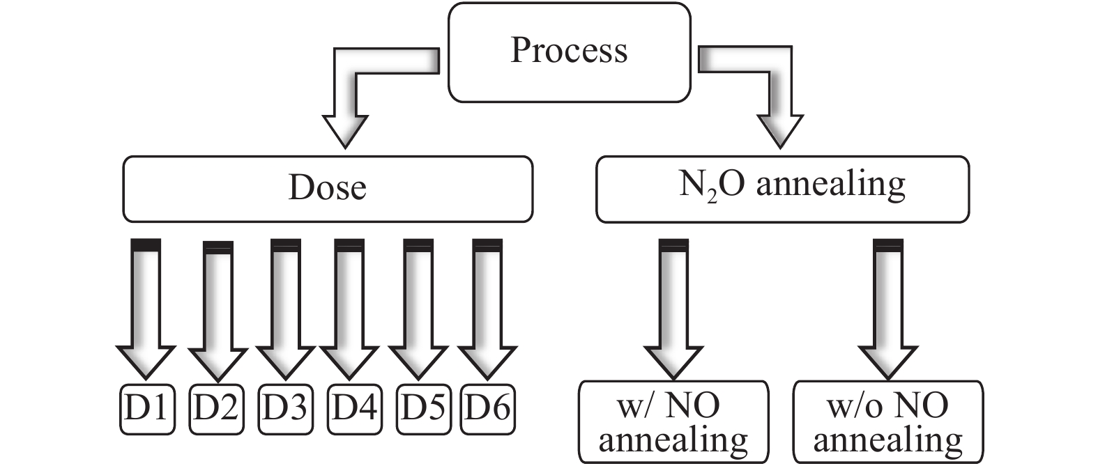
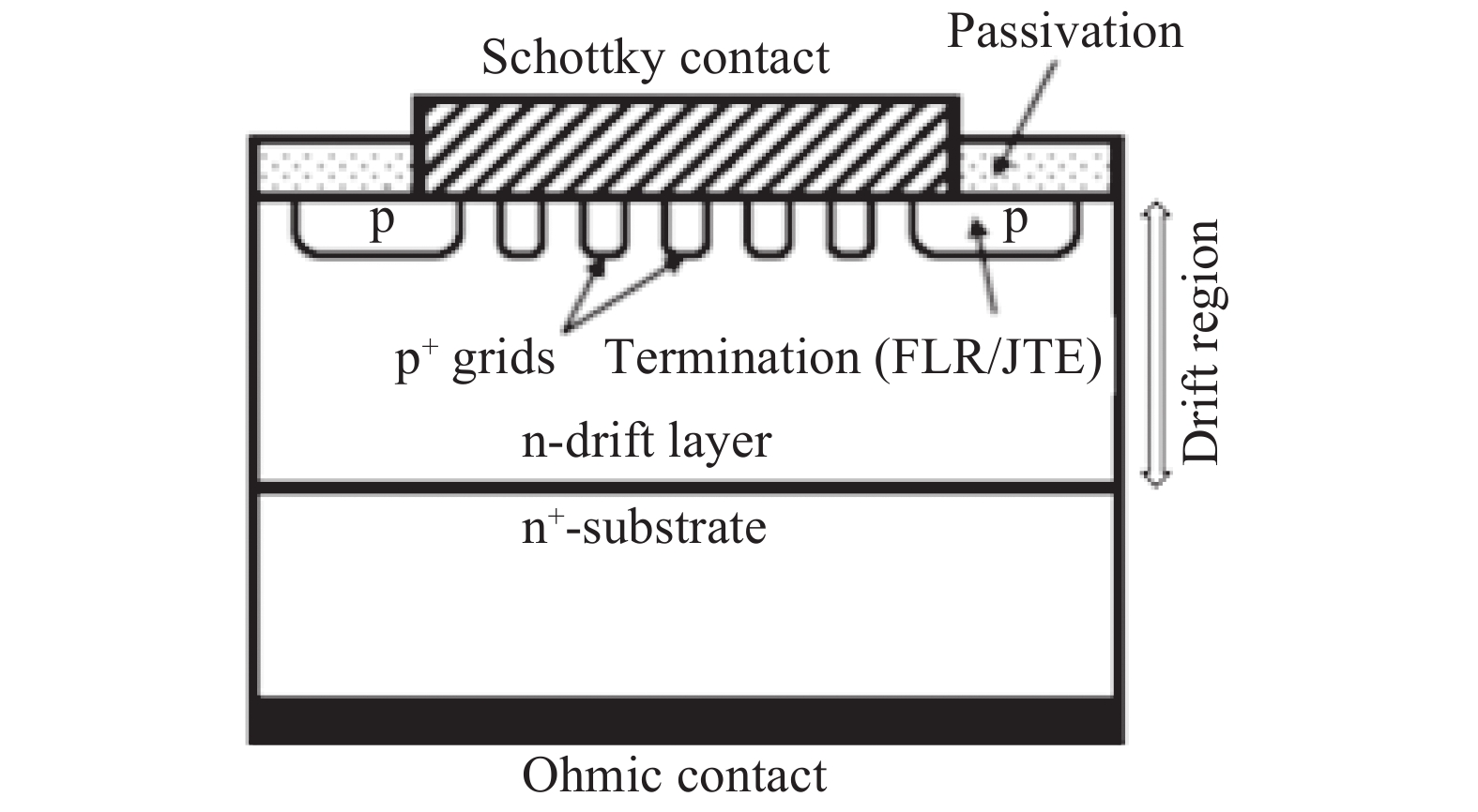
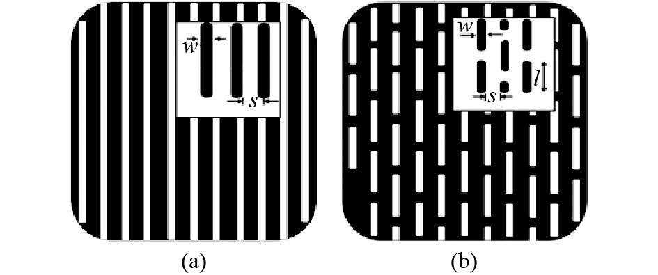
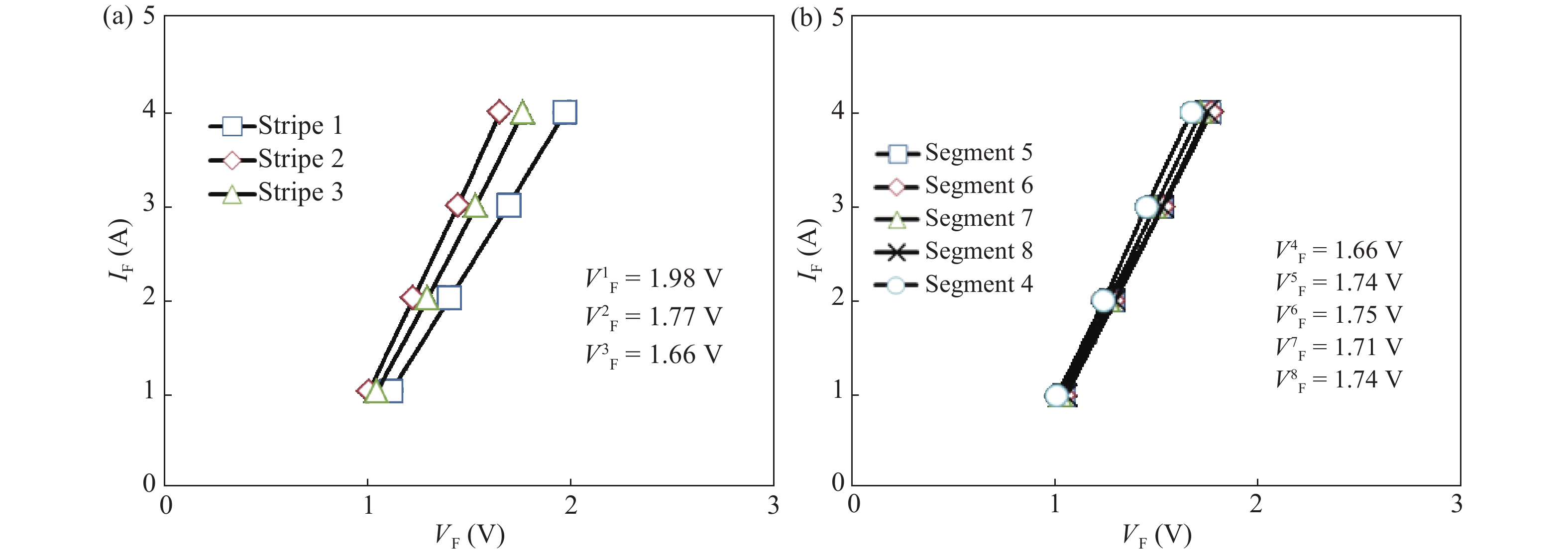
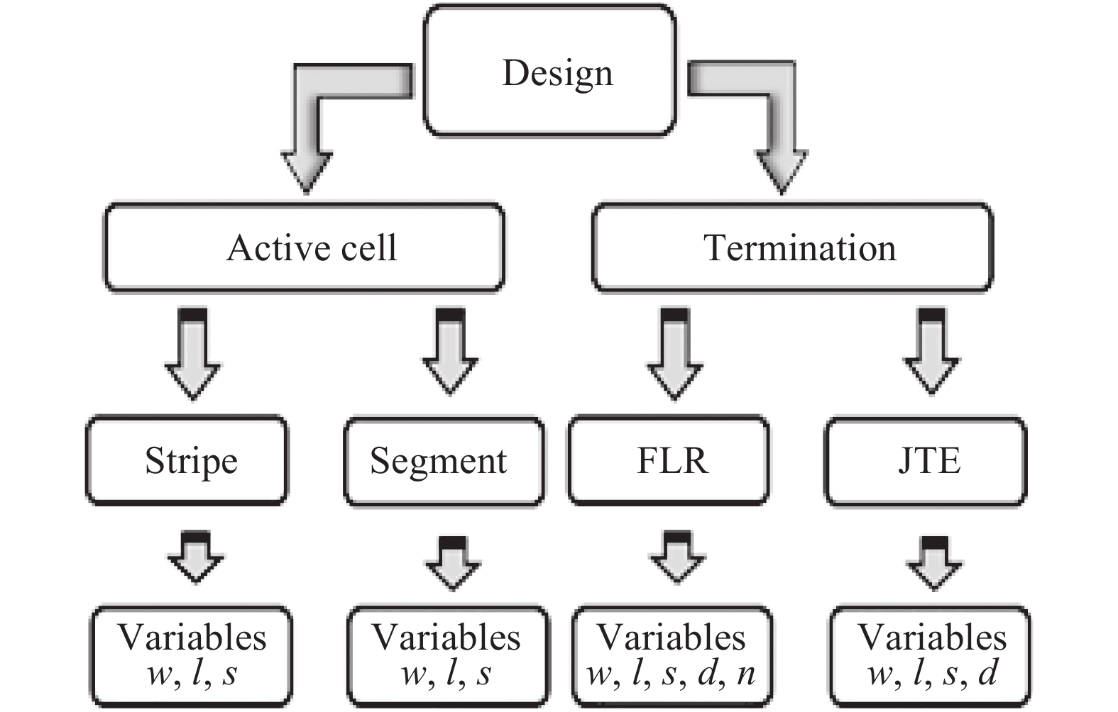
We have studied the influence of design and process variations on the electrical performance of SiC Schottky diodes. On the design side, two design variations are used in the active cell of the diode (segment design and stripe design). In addition, there are two more design variations employed for the edge termination layout of the diodes, namely, field limiting ring (FLR) and junction termination extension (JTE). On the process side, some diodes have gone through an N2O annealing step. The segment design resulted in a lower forward voltage drop (VF) in the diodes and the FLR design turned out to be a better choice for blocking voltages, in the reverse bias. Also, N2O annealing has shown a detrimental effect on the diodes’ blocking performance, which have JTE as their termination design. It degrades the blocking capability of the diodes significantly.-
Keywords:
- SiC,
- JBS diode,
- N2O annealing,
- hybrid SiC,
- IGBT
-
References
[1] Mikamura Y, Hiratsuka K, Tsuno T, et al. Novel designed SiC devices for high power and high efficiency systems. IEEE Trans Electron Devices, 2015, 62(2): 382 doi: 10.1109/TED.2014.2362537[2] Trew R J, Yan J B, Mock P M. The potential of diamond and SiC electronic devices for microwave and millimeter-wave power applications. Proc IEEE, 1991, 79(5): 598 doi: 10.1109/5.90128[3] Wondrak W, Held R, Niemann E, et al. SiC devices for advanced power and high-temperature applications. IEEE Trans Ind Electron, 2001, 48(2): 307 doi: 10.1109/41.915409[4] Mikamura Y, Hiratsuka K, Tsuno T, et al. Novel designed SiC devices for high power and high efficiency systems. IEEE Trans Electron Devices, 2015, 62(2): 382-9 doi: 10.1109/TED.2014.2362537[5] She X, Huang A Q, Lucía Ó, et al. Review of silicon carbide power devices and their applications. IEEE Trans Ind Electron, 2017, 64(10): 8193 doi: 10.1109/TIE.2017.2652401[6] Levinshtein M E, Rumyantsev S L, Shur M S. Properties of advanced semiconductor materials: GaN, AlN, InN, BN, SiC, SiGe. John Wiley & Sons, 2001[7] Millan J, Godignon P, Perpina X, et al. A survey of wide bandgap power semiconductor devices. IEEE Trans Power Electron, 2014, 29(5): 2155 doi: 10.1109/TPEL.2013.2268900[8] Kimoto T. Material science and device physics in SiC technology for high-voltage power devices. Jpn J Appl Phys, 2015, 54(4): 040103 doi: 10.7567/JJAP.54.040103[9] Shang F, Arribas A P, Krishnamurthy M. A comprehensive evaluation of SiC devices in traction applications. IEEE Transportation Electrification Conference and Expo, 2014: 5[10] Sharma Y. Advanced SiO2/SiC interface passivation. PhD Dissertain, Auburn University USA, 2012.[11] Zetterling C M. Process technology for silicon carbide devices. London: INSPEC, 2002[12] Kimoto T, Cooper J A. Fundamentals of silicon carbide technology: growth, characterization, devices and applications. John Wiley & Sons, 2014[13] Gao F, Weber W J, Posselt M, et al. Atomistic study of intrinsic defect migration in 3C-SiC. Phys Rev B, 2004, 69(24): 245205 doi: 10.1103/PhysRevB.69.245205[14] Morkoc H, Strite S, Gao G B, et al. Large-band-gap SiC, III–V nitride, and II–VI ZnSe-based semiconductor device technologies. J Appl Phys, 1994, 76(3): 1363 doi: 10.1063/1.358463[15] Ueno K, Oikawa T. Counter-doped MOSFETs of 4H-SiC. IEEE Electron Device Lett, 1999, 20(12): 624 doi: 10.1109/55.806105[16] Roccaforte F, Fiorenza P, Greco G, et al. Recent advances on dielectrics technology for SiC and GaN power devices. Appl Surf Sci, 2014, 301: 9 doi: 10.1016/j.apsusc.2014.01.063[17] Xu Y, Xu C, Liu G, et al. Concentration, chemical bonding, and etching behavior of P and N at the SiO2/SiC (0001) interface. J Appl Phys, 2015, 118(23): 235303 doi: 10.1063/1.4937400 -
Proportional views


 DownLoad:
