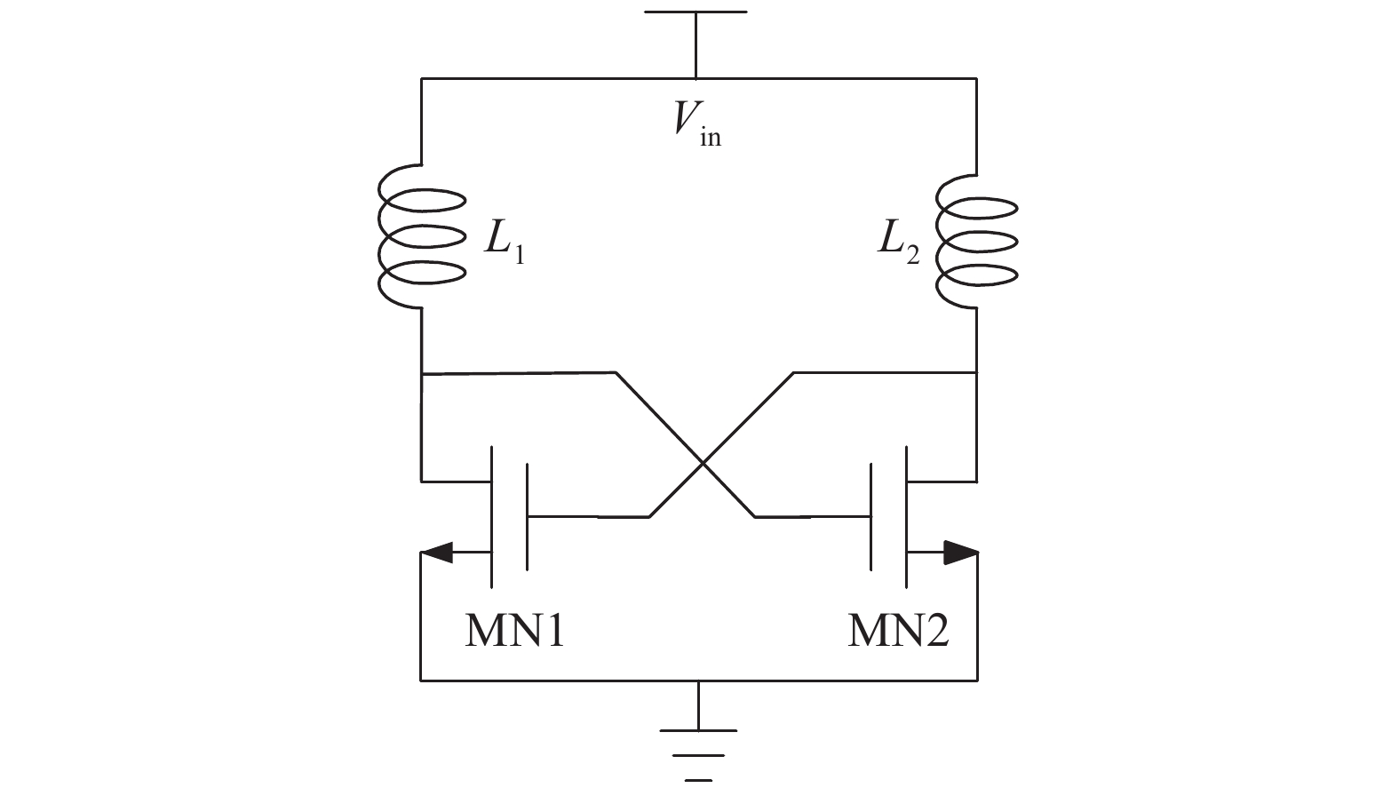
Processing math: 100%
J. Semicond. > 2018, Volume 39 > Issue 11 > 115003

SEMICONDUCTOR INTEGRATED CIRCUITS

4-port digital isolator based on on-chip transformer

Feng Zhang1, 2, Ting Zhao2, , Chunyu Ma2 and Dongfang Pan1

+ Author Affiliations

 Corresponding author: Ting Zhao, zhaot_dz@163.com

DOI: 10.1088/1674-4926/39/11/115003

PDF

Turn off MathJax

Abstract: The design and fabrication results of a 4-port digital isolator based on an on-chip transformer for galvanic isolation are presented. An ON–OFF keying modulation scheme is used to transmit the digital signal. The proposed digital isolator is fabricated by the 0.18 μm CMOS process. A test chip can achieve a 1 MHz signal bandwidth, a 40 ns propagation delay, a 35.5 mW input power and a 50 mA drive output current. The proposed digital isolator is pin-compatible, of small volume and low power replacement for the common 4-port optocoupler.

Key words: optocoupler4-portdigital isolatoron-chip transformer

Galvanic isolation is needed to protect systems and end users from potentially hazardous voltages in many applications including industrial control, military and space applications, medical electronics, and many others[1, 2]. Galvanic isolation can be achieved in multiple ways. Traditionally, optocouplers have been dominating the isolation market for their high isolation capability and relatively low cost. However, optocouplers have some intrinsic problems, such as low speed (1–50 Mbps), high power dissipation, degradation of the LED, and low common-mode transient immunity (CMTI). In addition, the performance of optocouplers is weakened by the changing of their current transfer ratio (CTR) with operating conditions and temperature.

Digital isolators fabricated in complementary metallic oxide semiconductor (CMOS) process technology are gaining favor from designers because of their significant advantages in terms of speed (100–150 Mbps), power dissipation, propagation delays, and more[3, 4]. Digital isolators using magnetic coupling[57], capacitive coupling[8, 9] and giant magneto resistive (GMR)[10] methods have been reported in the academic literature and commercially. They are challenging the optocouplers. However, the current digital isolators which usually provide six ports are not package- and pin-compatible to the common 4-port optocouplers. It can be difficult to replace optocouplers directly in some old designs.

In this paper, a 4-port digital isolator based on an on-chip transformer is proposed to supersede the 4-port optocoupler directly. The design can increase the signal bandwidth to 1 MHz and reduce the system volume and cost. The proposed digital isolator is suitable for the replacement of the common 4-port optocoupler, and it has higher signal bandwidth and lifetime. This paper is organized as follows. Section 2 describes the circuit schematic and design principles. Section 3 presents the simulation and measurement results, and finally conclusions are presented in Section 4.

Fig. 1 shows the block diagram of the proposed digital isolator. The system consists of a cross-coupled oscillator, an on-chip transformer, a demodulation module, and an open drain (OD) gate circuit. It provides four ports including INPUT, GND1, OUTPUT, and GND2, which is pin-compatible to the common 4-port optocoupler. The proposed digital isolator uses an ON–OFF keying (OOK) modulation scheme to transmit the digital logic signal. The oscillator sends a carrier signal across the transformer to represent one digital state, and sends no signal to represent the other digital state. The demodulation module demodulates the received signal. The OD gate circuit provides the drive current as the output.

Figure  1.  Block diagram of the proposed digital isolator.

Fig. 2 shows the circuit schematic. When Vin is greater than the threshold voltage of NMOS transistors, the carrier signal is generated by alternately turning on MN1 and MN2, and transmitted to the secondary side of the transformer. The received signal is demodulated by the full-wave bridge rectifier, and then OD gate circuit MN5 is charged until it is turned on. The output is connected to ground and Vout is set to low. When Vin is lower than the threshold voltage of NMOS transistors, the oscillator has no carrier signal by turning off the MN1 and MN2. The OD gate circuit is off. The output is connected to the supply voltage through the pull-up resistor RUP, and Vout is set to high.

Figure  2.  Circuit schematic of the proposed digital isolator.

It can be seen from the well known equation f = 1⁄(2π LC ) that L and C determine the oscillation frequency. Here, L is the equivalent inductance of the transformer, which is directly determined by the area of the transformer. C is the parasitic gate capacitance of the cross-coupled NMOS transistor. In order to satisfy the desired oscillation frequency, the on-chip transformer has been designed. In the case that the transformer area is limited to 500 μm2, the coil with more turns can gain greater inductance to reduce the switching loss. The on-chip stacked spirals transformer with its center tape connected to Vin is designed by the 3D finite element modeling (FEM) tool. The geometric parameters of the primary and secondary coil of the transformer include outer diameter (Dout), trace width (w), trace separation (s), thickness (t), and turns (N), as shown in Table 1. At 320 MHz, the simulated inductance and quality factor for primary and secondary coils are 216 nH, 262 nH, 2.1, and 1.1, respectively.

Table  1.  The geometric parameters of transformer.
Parameter Dout (μm) w (μm) s (μm) t (μm) N
Primary 500 5 0.6 0.87 32
Secondary 500 5 0.4 0.525 34
DownLoad: CSV  | Show Table

The on-chip transformer is implemented in a 0.18 μm CMOS process and the cross-section is shown in Fig. 3. A patterned ground shield (PGS) is used to improve the performance of the transformer. A 2.125 μm thick silicon dioxide and silicon nitride mixture is used as the insulating layer, which is tested to provide 0.4 kV isolation voltage.

Figure  3.  (Color online) Cross-sectional of transformer.

The schematic of the cross-coupled oscillator studied in this paper is shown in Fig. 4. Two CMOS transistors MN1 and MN2 implemented in a cross-coupled configuration together with transformer form the sustaining oscillation. L1 and L2 are the two primary inductors of the transformer.

Figure  4.  Cross-coupled oscillator.

The start-oscillating condition of the cross-coupled oscillator can be achieved by:

gm21R×α, (1)

where gm is the transconductance, R is the equivalent resistance of the primary coil, and α = 2–3 is the safety factor. The driving current provided by the CMOS transistor can be calculated by the Shichman-Hodge equation as follows:

ID=k(VgsVth)Vds+kV2ds2, (2)

where k is transistor gain, Vgs is gate-source voltage, Vds is drain-source voltage, and Vth is threshold voltage. At a 10 mA dynamic current, the width-to-length ratio of MN1 and MN2 are calculated as 100 μm/1.5 μm, and gm is calculated as 0.0998 s.

According to Ref. [11], it is assumed that only the first and the second harmonic of the output voltage are considered, the amplitude of the first harmonic is five times larger than the second harmonic, and thus the differential outputs of oscillator V and oscillation frequency f are given by:

V=2h1+2h1/5, (3)
f=1Tn=1LC{2π+4sin1[(VDDK0)/K1]}, (4)
K0=ξW4C4L, (5)

where h1 is the first harmonic amplitude. L is the equivalent inductance of the primary coil of the transformer. C is the parasitic gate capacitance of the cross-coupled NMOS transistor. VDD is the supply voltage. K1 is approximated by the first harmonic amplitude. ξ = 0.052 is a constant coefficient. W is the transistor width. The oscillation amplitude and oscillation frequency of the cross-coupled oscillator designed in this paper are calculated as 14.3 V and 327.3 MHz.

The demodulation module consists of rectifying circuit, discharge resistance Rg, and OD gate circuit. Both NMOS pairs and PMOS pairs are used as a rectifier. MN5 is an OD gate circuit which provides output drive current. The principle of the full-wave bridge rectifier is that if Vsp is positive, MN4 and MP1 are turned on, and if Vsn is positive, MN3 and MP2 are turned on. When Vg > VT, MN5 is turned on and the output is connected to ground and Vout is set to Low. When Vg < VT, MN5 is turned off and the output is connected to the supply voltage through RUP and Vout is set to High. The sizes of rectifier MOS transistors are decided by the output current of the rectifying circuit, which is given by:

Id=ΔVCΔt=VTCggRonCgg=VTRon, (6)

where VT = 800 mV is the threshold voltage of the OD gate circuit, Ron is the on-resistance of the rectifier MOS transistor, and Cgg is the gate oxide capacitance of the OD gate circuit. The size of OD gate circuit is designed according to 50 mA drive current. Therefore, the width-to-length ratio of MP1 (MP2), MN3 (MN4), and MN5 are designed as: 20 μm/0.5 μm, 70 μm/0.5 μm, and 40 μm/0.5 μm, respectively.

Fig. 5 shows the simulated waveform of the cross-coupled oscillator. The simulated oscillation amplitude and oscillation frequency are 15.8 V and 327.2 MHz. The simulated oscillating amplitude is greater than the calculated result. For the sake of simplicity, a higher order harmonic of the output voltage is neglected in the calculation.

Figure  5.  (Color online) Simulated waveform of the cross-coupled oscillator.

Fig. 6 shows the packaged chip, which is implemented in a 0.18 μm CMOS process. To measure the performance of the proposed digital isolator, the measurement setup is shown in Fig. 7. The signal is generated by Rigol DG5102.

Figure  6.  (Color online) Chip micrograph.
Figure  7.  Measurement setup.

Fig. 8 shows the measured input and output waveforms at the operating condition (VDD = 5 V @ 1 MHz, Rup = 1 kΩ). The chip operates in a supply range from 4.5 to 5.5 V with a maximum propagation delay of 40 ns.

Figure  8.  (Color online) Measured input and output waveforms.

Table 2 summarizes the performance of the proposed digital isolator and compares it to other optocouplers[12, 13]. A 50 mA drive output current is realized. The input current and input power consumption is the smallest, and the signal bandwidth is 1 MHz higher than PC817. While the isolation voltage of this design is only 0.4 kVrms, it can be improved by choosing a thicker isolation layer or other isolation materials with higher breakdown voltage.

Table  2.  Performance summary.
Performance This work Ref. [12] Ref. [13]
Input current (mA) 7.1 50 80
Output current (mA) 50 50 50
Signal bandwidth (MHz) 1 0.08 1
Input power consumption (mW) 35.5 70 120
Isolation voltage (kVrms) 0.4 5 5
DownLoad: CSV  | Show Table

A 4-port digital isolator based on an on-chip transformer is designed and fabricated in 0.18 μm CMOS process. By testing and certification, the chip has advantages of lower power consumption, higher bandwidth, and smaller volume than other optocouplers. While the isolation voltage of the chip is lower than other optocouplers, there is a lot of room for improvement. The proposed digital isolator can reduce the total system complexity and cost. It is very convenient and economical to replace the common 4-port optocoupler directly in some old designs.


[1]
Kaeriyama S, Uchida S, Furumiya M, et al. A 2.5 kV isolation 35 kV/μs CMR 250 Mbps digital isolator in standard CMOS with a small transformer driving technique. IEEE J Solid-State Circuits, 2012, 47(2): 435 doi: 10.1109/JSSC.2011.2170775
[2]
Coyne E, Lynch S, McGuinness P, et al. Low gate drive IGBT enabling direct control through digital isolator power. IEEE Symposium on Bipolar/BiCMOS Circuits and Technology Meeting, New Brunswick, NJ, USA, 2016: 134
[3]
Fandrich C L. An on-chip transformer-based digital isolator system. Master's thesis. The University of Tennessee, Knoxville, USA, 2013
[4]
Lumio M. Applicability of CMOS digital isolators in variable-frequency drives. Master's Thesis, Aalto University, Finland, 2016
[5]
Uchida S, Kaeriyama S, Nagase H, et al. A face-to-face chip stacking 7 kV RMS digital isolator for automotive and industrial motor drive applications. IEEE 26th International Symposium on Power Semiconductor Devices & IC's, Waikoloa, Hawaii, 2014: 442
[6]
Yun R, Sun J, Gaalaas E, et al. A transformer-based digital isolator with 20 kV PK surge capability and > 200 kV/ μS common mode transient immunity. IEEE Symposium on VLSI Circuits, Honolulu, Hawaii, USA, 2016: 1
[7]
To D N, Rouger N, Lembeye Y, et al. Modeling and characterization of 0.35 μm CMOS coreless transformer for gate drivers. IEEE 26th International Symposium on Power Semiconductor Devices & IC's, Waikoloa, Hawaii, USA, 2014: 330
[8]
Culurciello E, Pouliquen P O, Andreou A G. Digital isolation amplifier in silicon-on-sapphire CMOS. Electron Lett, 2007, 43(8): 451 doi: 10.1049/el:20070509
[9]
Moghe Y, Terry A, Luzon D. Monolithic 2.5 kV RMS, 1.8–3.3 V dual-channel 640 Mbps digital isolator in 0.5 μm SOS. IEEE International SOI Conference, Napa, California, USA, 2012: 1
[10]
Park S, Kim J, Jo S. Modeling of giant magnetoresistance isolator for high speed digital data transmission utilizing spin valves. J Appl Phys, 2005, 97(10): 2773
[11]
Daliri M, Maymandi-Nejad M. Analytical model for CMOS cross-coupled LC-tank oscillator. IET Circuits, Devices Syst, 2013, 8(1): 1
[12]
PC817 Series, High density mounting type photocoupler, Data Sheet, SHARP
[13]
PS2501-1,-2,-4,PS2501l-1,-2,-4, High isolation voltage single transistor type multi photocoupler series, Data Sheet PN10225EJ03V0DS, NEC
Fig. 1.  Block diagram of the proposed digital isolator.

Fig. 2.  Circuit schematic of the proposed digital isolator.

Fig. 3.  (Color online) Cross-sectional of transformer.

Fig. 4.  Cross-coupled oscillator.

Fig. 5.  (Color online) Simulated waveform of the cross-coupled oscillator.

Fig. 6.  (Color online) Chip micrograph.

Fig. 7.  Measurement setup.

Fig. 8.  (Color online) Measured input and output waveforms.

Table 1.   The geometric parameters of transformer.

Parameter Dout (μm) w (μm) s (μm) t (μm) N
Primary 500 5 0.6 0.87 32
Secondary 500 5 0.4 0.525 34
DownLoad: CSV

Table 2.   Performance summary.

Performance This work Ref. [12] Ref. [13]
Input current (mA) 7.1 50 80
Output current (mA) 50 50 50
Signal bandwidth (MHz) 1 0.08 1
Input power consumption (mW) 35.5 70 120
Isolation voltage (kVrms) 0.4 5 5
DownLoad: CSV
[1]
Kaeriyama S, Uchida S, Furumiya M, et al. A 2.5 kV isolation 35 kV/μs CMR 250 Mbps digital isolator in standard CMOS with a small transformer driving technique. IEEE J Solid-State Circuits, 2012, 47(2): 435 doi: 10.1109/JSSC.2011.2170775
[2]
Coyne E, Lynch S, McGuinness P, et al. Low gate drive IGBT enabling direct control through digital isolator power. IEEE Symposium on Bipolar/BiCMOS Circuits and Technology Meeting, New Brunswick, NJ, USA, 2016: 134
[3]
Fandrich C L. An on-chip transformer-based digital isolator system. Master's thesis. The University of Tennessee, Knoxville, USA, 2013
[4]
Lumio M. Applicability of CMOS digital isolators in variable-frequency drives. Master's Thesis, Aalto University, Finland, 2016
[5]
Uchida S, Kaeriyama S, Nagase H, et al. A face-to-face chip stacking 7 kV RMS digital isolator for automotive and industrial motor drive applications. IEEE 26th International Symposium on Power Semiconductor Devices & IC's, Waikoloa, Hawaii, 2014: 442
[6]
Yun R, Sun J, Gaalaas E, et al. A transformer-based digital isolator with 20 kV PK surge capability and > 200 kV/ μS common mode transient immunity. IEEE Symposium on VLSI Circuits, Honolulu, Hawaii, USA, 2016: 1
[7]
To D N, Rouger N, Lembeye Y, et al. Modeling and characterization of 0.35 μm CMOS coreless transformer for gate drivers. IEEE 26th International Symposium on Power Semiconductor Devices & IC's, Waikoloa, Hawaii, USA, 2014: 330
[8]
Culurciello E, Pouliquen P O, Andreou A G. Digital isolation amplifier in silicon-on-sapphire CMOS. Electron Lett, 2007, 43(8): 451 doi: 10.1049/el:20070509
[9]
Moghe Y, Terry A, Luzon D. Monolithic 2.5 kV RMS, 1.8–3.3 V dual-channel 640 Mbps digital isolator in 0.5 μm SOS. IEEE International SOI Conference, Napa, California, USA, 2012: 1
[10]
Park S, Kim J, Jo S. Modeling of giant magnetoresistance isolator for high speed digital data transmission utilizing spin valves. J Appl Phys, 2005, 97(10): 2773
[11]
Daliri M, Maymandi-Nejad M. Analytical model for CMOS cross-coupled LC-tank oscillator. IET Circuits, Devices Syst, 2013, 8(1): 1
[12]
PC817 Series, High density mounting type photocoupler, Data Sheet, SHARP
[13]
PS2501-1,-2,-4,PS2501l-1,-2,-4, High isolation voltage single transistor type multi photocoupler series, Data Sheet PN10225EJ03V0DS, NEC
1

A 130-nm ferroelectric nonvolatile system-on-chip for internet of things

Zhiyi Yu

Journal of Semiconductors, 2019, 40(2): 020205. doi: 10.1088/1674-4926/40/2/020205

2

245 GHz subharmonic receiver with on-chip antenna for gas spectroscopy application

Yanfei Mao, Shiju E, Klaus Schmalz, J. Christoph Scheytt

Journal of Semiconductors, 2018, 39(12): 125001. doi: 10.1088/1674-4926/39/12/125001

3

In situ TEM/SEM electronic/mechanical characterization of nano material with MEMS chip

Yuelin Wang, Tie Li, Xiao Zhang, Hongjiang Zeng, Qinhua Jin, et al.

Journal of Semiconductors, 2014, 35(8): 081001. doi: 10.1088/1674-4926/35/8/081001

4

VCCS controlled LDO with small on-chip capacitor

Qiuli Li, Yao Qian, Danzhu Lü, Zhiliang Hong

Journal of Semiconductors, 2014, 35(11): 115011. doi: 10.1088/1674-4926/35/11/115011

5

A 10 MHz ripple-based on-time controlled buck converter with dual ripple compensation

Danzhu Lü, Jiale Yu, Zhiliang Hong

Journal of Semiconductors, 2013, 34(2): 025005. doi: 10.1088/1674-4926/34/2/025005

6

Power-aware transceiver design for half-duplex bidirectional chip-to-chip optical interconnects

Jamshid Sangirov, Ikechi Augustine Ukaegbu, Gulomjon Sangirov, Tae-Woo Lee, Hyo-Hoon Park, et al.

Journal of Semiconductors, 2013, 34(12): 125001. doi: 10.1088/1674-4926/34/12/125001

7

Characterization of electrical properties of AlGaN/GaN interface using coupled Schrödinger and Poisson equation

S. Das, A. K. Panda, G. N. Dash

Journal of Semiconductors, 2012, 33(11): 113001. doi: 10.1088/1674-4926/33/11/113001

8

Chaotic dynamics dependence on doping density in weakly coupled GaAs/AlAs superlattices

Yang Gui, Li Yuanhong, Zhang Fengying, Li Yuqi

Journal of Semiconductors, 2012, 33(9): 092002. doi: 10.1088/1674-4926/33/9/092002

9

Double-π fully scalable model for on-chip spiral inductors

Liu Jun, Zhong Lin, Wang Huang, Wen Jincai, Sun Lingling, et al.

Journal of Semiconductors, 2012, 33(8): 084007. doi: 10.1088/1674-4926/33/8/084007

10

A robust and simple two-mode digital calibration technique for pipelined ADC

Yin Xiumei, Zhao Nan, Sekedi Bomeh Kobenge, Yang Huazhong

Journal of Semiconductors, 2011, 32(3): 035001. doi: 10.1088/1674-4926/32/3/035001

11

Development of spin-on-glass process for triple metal interconnects

Peng Li, Zhao Wenbin, Wang Guozhang, Yu Zongguang

Journal of Semiconductors, 2010, 31(12): 126003. doi: 10.1088/1674-4926/31/12/126003

12

Full on-chip and area-efficient CMOS LDO with zero to maximum load stability using adaptive frequency compensation

Ma Haifeng, Zhou Feng

Journal of Semiconductors, 2010, 31(1): 015006. doi: 10.1088/1674-4926/31/1/015006

13

An asymmetric MOSFET-C band-pass filter with on-chip charge pump auto-tuning

Chen Fangxiong, Lin Min, Ma Heping, Jia Hailong, Shi Yin, et al.

Journal of Semiconductors, 2009, 30(8): 085005. doi: 10.1088/1674-4926/30/8/085005

14

A novel on-chip high to low voltage power conversion circuit

Wang Hui, Wang Songlin, Lai Xinquan, Ye Qiang, Mou Zaixin, et al.

Journal of Semiconductors, 2009, 30(3): 035008. doi: 10.1088/1674-4926/30/3/035008

15

Design and performance of a complex-coupled DFB laser with sampled grating

Wang Huan, Zhu Hongliang, Jia Linghui, Chen Xiangfei, Wang Wei, et al.

Journal of Semiconductors, 2009, 30(2): 024003. doi: 10.1088/1674-4926/30/2/024003

16

Monolithically Integrated Optoelectronic Receivers Implemented in 0.25μm MS/RF CMOS

Chen Hongda, Gao Peng, Mao Luhong, Huang Jiale

Chinese Journal of Semiconductors , 2006, 27(2): 323-327.

17

12Gb/s 0.25μm CMOS Low-Power 1∶4 Demultiplexer

Ding Jingfeng, Wang Zhigong, Zhu En, Zhang Li, Wang Gui, et al.

Chinese Journal of Semiconductors , 2006, 27(1): 19-23.

18

Full-Chip Scalable Routing Framework Considering Congestion and Performance

Yao Hailong, Cai Yici, Hong Xianlong, Zhou Qiang

Chinese Journal of Semiconductors , 2006, 27(7): 1201-1208.

19

A 1×4 Polymeric Digital Optical Switch Basedon the Thermo-Optic Effect

Tang Yi, Zhang Hao, Yang Jianyi, Wang Minghua, Jiang Xiaoqing, et al.

Chinese Journal of Semiconductors , 2006, 27(4): 692-695.

20

Transport Properties of Two Coupled Quantum Dots Under Optical Pumping

Ge Chuannan, Wen Jun, Peng Ju, Wang Baigeng

Chinese Journal of Semiconductors , 2006, 27(4): 598-603.

1. Zhang, J., Zhang, B., Zhang, Q. et al. Scalable Galvanic Isolators with High Isolation Realized by Magnetoelectric Gyrators. Journal of Electronic Materials, 2022. doi:10.1007/s11664-022-10135-6
2. Zhang, F., Ma, C., Zhao, T. An expression for oscillation amplitude of NMOS/PMOS complementary cross-coupled LC-tank oscillator. 2019. doi:10.1109/EDSSC.2019.8754367
  • Search

    Advanced Search >>

    GET CITATION

    Feng Zhang, Ting Zhao, Chunyu Ma, Dongfang Pan. 4-port digital isolator based on on-chip transformer[J]. Journal of Semiconductors, 2018, 39(11): 115003. doi: 10.1088/1674-4926/39/11/115003
    F Zhang, T Zhao, C Y Ma, D F Pan, 4-port digital isolator based on on-chip transformer[J]. J. Semicond., 2018, 39(11): 115003. doi: 10.1088/1674-4926/39/11/115003.
    shu

    Export: BibTex EndNote

    Article Metrics

    Article views: 4001 Times PDF downloads: 92 Times Cited by: 2 Times

    History

    Received: 28 February 2018 Revised: 22 April 2018 Online: Uncorrected proof: 28 June 2018Published: 01 November 2018

    Catalog

      Email This Article

      User name:
      Email:*请输入正确邮箱
      Code:*验证码错误
      Feng Zhang, Ting Zhao, Chunyu Ma, Dongfang Pan. 4-port digital isolator based on on-chip transformer[J]. Journal of Semiconductors, 2018, 39(11): 115003. doi: 10.1088/1674-4926/39/11/115003 ****F Zhang, T Zhao, C Y Ma, D F Pan, 4-port digital isolator based on on-chip transformer[J]. J. Semicond., 2018, 39(11): 115003. doi: 10.1088/1674-4926/39/11/115003.
      Citation:
      Feng Zhang, Ting Zhao, Chunyu Ma, Dongfang Pan. 4-port digital isolator based on on-chip transformer[J]. Journal of Semiconductors, 2018, 39(11): 115003. doi: 10.1088/1674-4926/39/11/115003 ****
      F Zhang, T Zhao, C Y Ma, D F Pan, 4-port digital isolator based on on-chip transformer[J]. J. Semicond., 2018, 39(11): 115003. doi: 10.1088/1674-4926/39/11/115003.

      4-port digital isolator based on on-chip transformer

      DOI: 10.1088/1674-4926/39/11/115003
      More Information
      • Corresponding author: zhaot_dz@163.com
      • Received Date: 2018-02-28
      • Revised Date: 2018-04-22
      • Published Date: 2018-11-01

      Catalog

        /

        DownLoad:  Full-Size Img  PowerPoint
        Return
        Return