


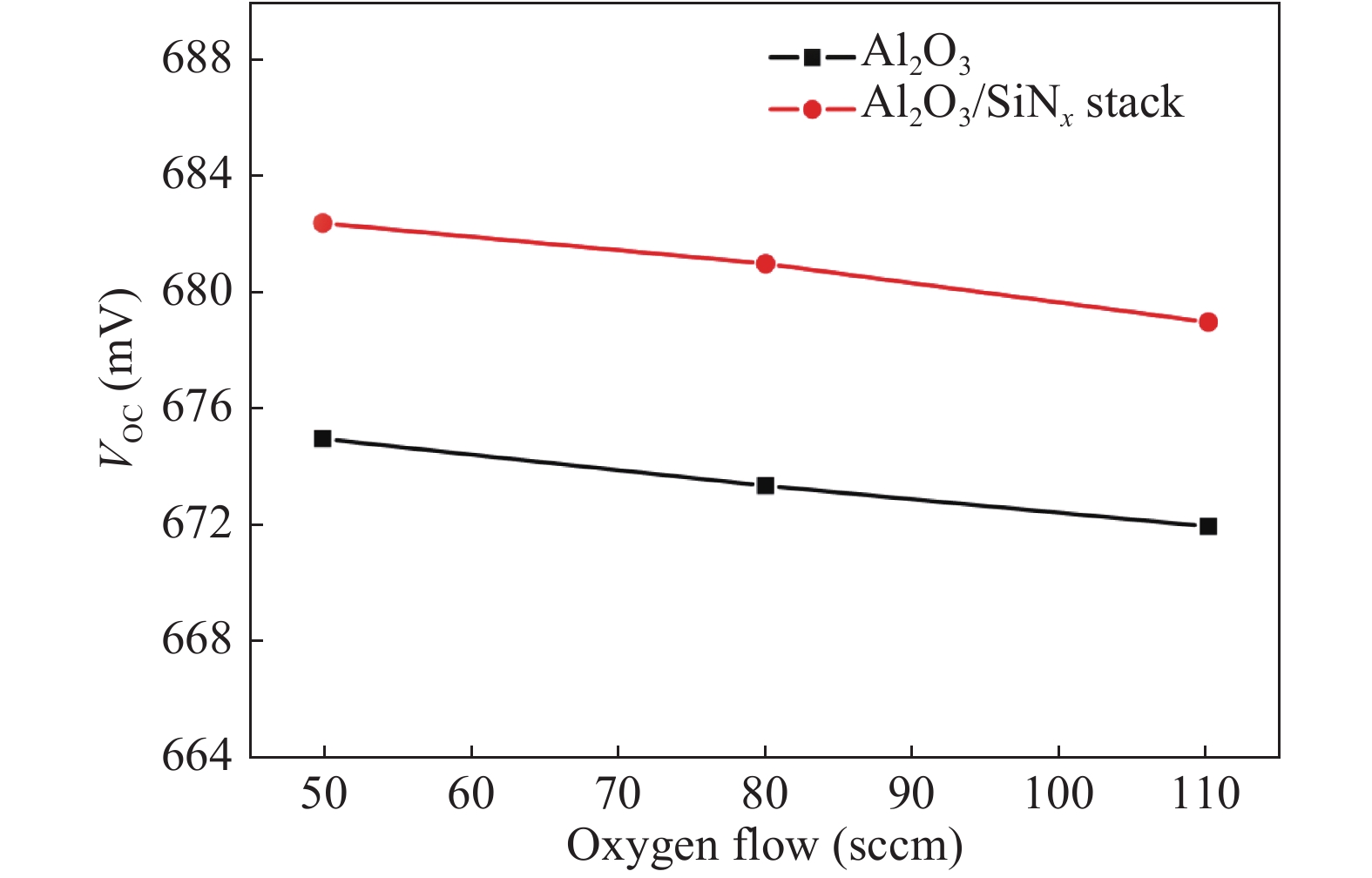
Fig. 1.
(Color online) The implied Voc of group III samples driven-in under different O2 flows of 50, 80, and 110 sccm, respectively.
SEMICONDUCTOR PHYSICS
Caixia Hou1, 2, Rui Jia2, , Ke Tao2, Shuai Jiang2, Pengfei Zhang2, Hengchao Sun2, Sanjie Liu1, Mingzeng Peng1, and Xinhe Zheng1,
Corresponding author: Rui Jia, E-mail: jiarui@ime.ac.cn; Mingzeng Peng, mzpeng@ustb.edu.cn; Xinhe Zheng, xinhezheng@ustb.edu.cn
Abstract: In boron-doped p+–n crystalline silicon (Si) solar cells, p-type boron doping control and surface passivation play a vital role in the realization of high-efficiency and low cost pursuit. In this study, boron-doped p+-emitters are formed by boron diffusion in an open-tube furnace using borontribromide (BBr3) as precursor. The formed emitters are characterized in detail in terms of shape of the doping profile, surface doping concentration, junction depth, sheet resistance and removal of the boron-rich layer (BRL). In the aspect of BRL removal, three different methods were adopted to investigate their influence on device performance. The results demonstrate that our proposed chemical etch treatment (CET) with the proper etching time could be an effective way to remove the BRL. After removal of the BRL, Al2O3/SiNx stacks are deposited by atomic layer deposition (ALD) and plasma-enhanced chemical vapor deposition (PECVD) to passivate the cell surface. It was found that a reasonably-high implied Voc of 680 mV has been achieved for the fabricated n-type Si solar cells.
Keywords: p+–n Si solar cell, boron-rich layer, Al2O3/SiNx stack, surface passivation
| [1] |
Glunz S W, Rein S, Lee J Y, et al. Minority carrier lifetime degradation in boron-doped Czochralski silicon. J Appl Phys, 2001, 90(5): 2397 doi: 10.1063/1.1389076
|
| [2] |
Cotter J E, Guo J H, Cousins P J, et al. P-type versus n-type silicon wafers: prospects for high-efficiency commercial silicon solar cells. IEEE Trans Electron Devices, 2006, 53(8): 1893 doi: 10.1109/TED.2006.878026
|
| [3] |
Zhao J, Wang A, Altermatt P P, et al. High efficiency PERT cells on n-type silicon substrates. Photovoltaic Specialists Conference (PVSC), Conference Record of the Twenty-Ninth IEEE, 2002: 218.
|
| [4] |
Kiefer F, Ulzhöfer C, Brendemühl T, et al. High efficiency n-type emitter-wrap-through silicon solar cells. IEEE J Photovolt, 2011, 1(1): 49 doi: 10.1109/JPHOTOV.2011.2164953
|
| [5] |
Benick J, Hoex B, Van de Sanden M C M, et al. High efficiency n-type Si solar cells on Al2O3-passivated boron emitters. Appl Phys Lett, 2008, 92(25): 253504 doi: 10.1063/1.2945287
|
| [6] |
Book F, Wiedenmann T, Schubert G, et al. Influence of the front surface passivation quality on large area n-type silicon solar cells with Al-alloyed rear emitter. Energy Procedia, 2011, 8: 487
|
| [7] |
Macdonald D, Geerligs L J. Recombination activity of interstitial iron and other transition metal point defects in p-and n-type crystalline silicon. Appl Phys Lett, 2004, 85(18): 4061 doi: 10.1063/1.1812833
|
| [8] |
Das A, Ryu K, Rohatgi A. 20% efficient screen-printed n-type solar cells using a spin-on source and thermal oxide/silicon nitride passivation. IEEE J Photovolt, 2011, 1(2): 146 doi: 10.1109/JPHOTOV.2011.2172189
|
| [9] |
Meier D L, Chandrasekaran V, Davis H P, et al. N-type ion-implanted silicon solar cells and modules. IEEE J Photovolt, 2011, 1(2): 123 doi: 10.1109/JPHOTOV.2011.2169944
|
| [10] |
Rohatgi A, Meier D L, McPherson B, et al. High-throughput ion-implantation for low-cost high-efficiency silicon solar cells. Energy Procedia, 2012, 15: 10 doi: 10.1016/j.egypro.2012.02.002
|
| [11] |
Ryu K, Upadhyaya A, Ok Y W, et al. High-efficiency n-type Si solar cells with novel inkjet-printed boron mitters. IEEE Electron Device Lett, 2012, 33(6): 854 doi: 10.1109/LED.2012.2191263
|
| [12] |
Bazer-Bachi B, Oliver C, Semmache B, et al. Co-diffusion from boron doped oxide and POCl3. Proceedings of the 26th European Photovoltaic Solar Energy Conference and Exhibition, 2011: 1155.
|
| [13] |
Bartholomew L D, Gralenski N M, Sisson J C, et al. Doped SiO2 deposition from TMP in APCVD. Eu Trans Telecommun, 1990, 1(2): 167 doi: 10.1002/ett.v1:2
|
| [14] |
Rothhardt P, Demberger C, Wolf A, et al. Co-diffusion from APCVD BSG and POCl3 for industrial n-type solar cells. Energy Procedia, 2013, 38: 305 doi: 10.1016/j.egypro.2013.07.282
|
| [15] |
Pawlak B J, Janssens T, Singh S, et al. Studies of implanted boron emitters for solar cell applications. Prog Photovolts: Res Appl, 2012, 20(1): 106 doi: 10.1002/pip.v20.1
|
| [16] |
Spitzer M B, Keavney C J. Attainment of transparent boron-implanted layers for silicon solar cell applications. Appl Phys Lett, 1985, 47(7): 731 doi: 10.1063/1.96019
|
| [17] |
Armand J, Oliver C, Semmache B, et al. Modelling and analysis of the emitter boron process under BCl3 and O2 for industrial silicon solar cells applications. Proceedings of 26th European Photovoltaic Solar Energy Conference and Exhibition, 2011: 1309.
|
| [18] |
Mehrer H. Diffusion of interstitial solutes in metals. Diffusion in Solids: Fundamentals, Methods, Materials, Diffusion-Controlled Processes, 2007: 313
|
| [19] |
Myers S M, Seibt M, Schröter W. Mechanisms of transition-metal gettering in silicon. J Appl Phys, 2000, 88(7): 3795 doi: 10.1063/1.1289273
|
| [20] |
Ning X J. Distribution of residual stresses in boron doped p+ silicon films. J Electrochem Soc, 1996, 143(10): 3389 doi: 10.1149/1.1837217
|
| [21] |
Cousins P J, Cotter J E. The influence of diffusion-induced dislocations on high efficiency silicon solar cells. IEEE Trans Electron Devices, 2006, 53(3): 457 doi: 10.1109/TED.2005.863535
|
| [22] |
Kessler M A, Ohrdes T, Wolpensinger B, et al. Charge carrier lifetime degradation in Cz silicon through the formation of a boron-rich layer during BBr3 diffusion processes. Semicond Sci Technol, 2010, 25(5): 055001 doi: 10.1088/0268-1242/25/5/055001
|
| [23] |
Macdonald D, Mäckel H, Cuevas A. Effect of gettered iron on recombination in diffused regions of crystalline silicon wafers. Appl Phys Lett, 2006, 88(9): 092105 doi: 10.1063/1.2181199
|
| [24] |
Libal J, Petres R, Buck T, et al. N-type multicrystalline silicon solar cells: BBr3-diffusion and passivation of p+-diffused silicon surfaces. 20th European Photovoltaic Solar Energy Conference, 2005: 793
|
| [25] |
Phang S P, Macdonald D. Direct comparison of boron, phosphorus, and aluminum gettering of iron in crystalline silicon. J Appl Phys, 2011, 109(7): 073521 doi: 10.1063/1.3569890
|
| [26] |
Schmidt J, Bothe K, Bock R, et al. n-type silicon-the better material choice for industrial high-efficiency solar cells. Proceedings of the 22th European Photovoltaic Solar Energy Conference and Exhibition, 2007: 998
|
| [27] |
Istratov A A, Buonassisi T, McDonald R J, et al. Metal content of multicrystalline silicon for solar cells and its impact on minority carrier diffusion length. J Appl Phys, 2003, 94(10): 6552 doi: 10.1063/1.1618912
|
| [28] |
Nanver L K, Qi L, Mohammadi V, et al. Robust UV/VUV/EUV PureB photodiode detector technology with high CMOS compatibility. IEEE Sel Topics Quantum Electron, 2014, 20(6): 306 doi: 10.1109/JSTQE.2014.2319582
|
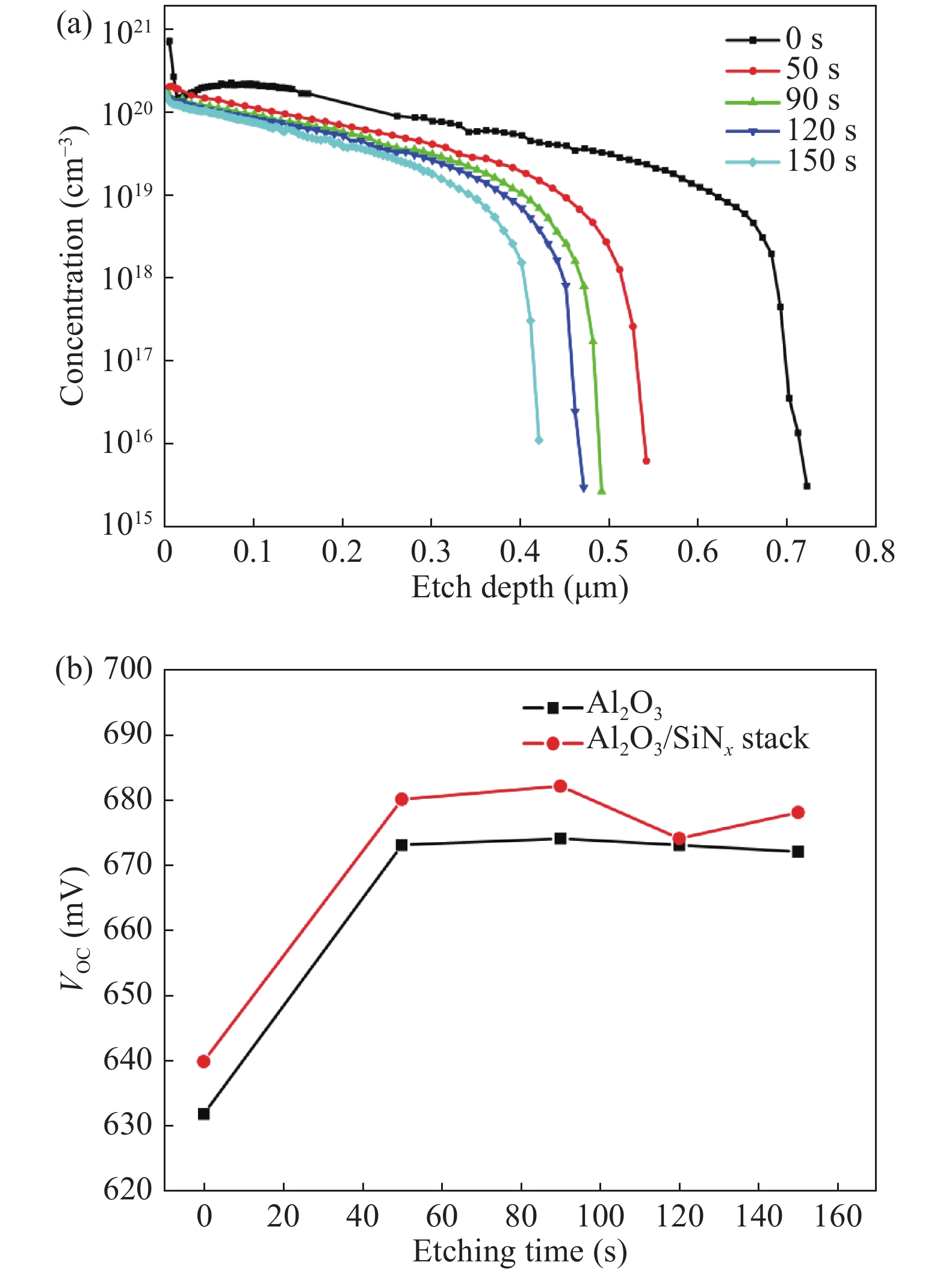
Table 1. Sheet resistances and junction depth for different CET times.
| Etched time (s) | 0 | 50 | 90 | 120 | 150 |
| Sheet resistance (Ω/sq) | 19.65 | 34.15 | 42.72 | 47.39 | 54.69 |
| Junction depth (nm) | 700.0 | 565.6 | 495.5 | 474.6 | 450.2 |
 DownLoad: CSV
| [1] |
Glunz S W, Rein S, Lee J Y, et al. Minority carrier lifetime degradation in boron-doped Czochralski silicon. J Appl Phys, 2001, 90(5): 2397 doi: 10.1063/1.1389076
|
| [2] |
Cotter J E, Guo J H, Cousins P J, et al. P-type versus n-type silicon wafers: prospects for high-efficiency commercial silicon solar cells. IEEE Trans Electron Devices, 2006, 53(8): 1893 doi: 10.1109/TED.2006.878026
|
| [3] |
Zhao J, Wang A, Altermatt P P, et al. High efficiency PERT cells on n-type silicon substrates. Photovoltaic Specialists Conference (PVSC), Conference Record of the Twenty-Ninth IEEE, 2002: 218.
|
| [4] |
Kiefer F, Ulzhöfer C, Brendemühl T, et al. High efficiency n-type emitter-wrap-through silicon solar cells. IEEE J Photovolt, 2011, 1(1): 49 doi: 10.1109/JPHOTOV.2011.2164953
|
| [5] |
Benick J, Hoex B, Van de Sanden M C M, et al. High efficiency n-type Si solar cells on Al2O3-passivated boron emitters. Appl Phys Lett, 2008, 92(25): 253504 doi: 10.1063/1.2945287
|
| [6] |
Book F, Wiedenmann T, Schubert G, et al. Influence of the front surface passivation quality on large area n-type silicon solar cells with Al-alloyed rear emitter. Energy Procedia, 2011, 8: 487
|
| [7] |
Macdonald D, Geerligs L J. Recombination activity of interstitial iron and other transition metal point defects in p-and n-type crystalline silicon. Appl Phys Lett, 2004, 85(18): 4061 doi: 10.1063/1.1812833
|
| [8] |
Das A, Ryu K, Rohatgi A. 20% efficient screen-printed n-type solar cells using a spin-on source and thermal oxide/silicon nitride passivation. IEEE J Photovolt, 2011, 1(2): 146 doi: 10.1109/JPHOTOV.2011.2172189
|
| [9] |
Meier D L, Chandrasekaran V, Davis H P, et al. N-type ion-implanted silicon solar cells and modules. IEEE J Photovolt, 2011, 1(2): 123 doi: 10.1109/JPHOTOV.2011.2169944
|
| [10] |
Rohatgi A, Meier D L, McPherson B, et al. High-throughput ion-implantation for low-cost high-efficiency silicon solar cells. Energy Procedia, 2012, 15: 10 doi: 10.1016/j.egypro.2012.02.002
|
| [11] |
Ryu K, Upadhyaya A, Ok Y W, et al. High-efficiency n-type Si solar cells with novel inkjet-printed boron mitters. IEEE Electron Device Lett, 2012, 33(6): 854 doi: 10.1109/LED.2012.2191263
|
| [12] |
Bazer-Bachi B, Oliver C, Semmache B, et al. Co-diffusion from boron doped oxide and POCl3. Proceedings of the 26th European Photovoltaic Solar Energy Conference and Exhibition, 2011: 1155.
|
| [13] |
Bartholomew L D, Gralenski N M, Sisson J C, et al. Doped SiO2 deposition from TMP in APCVD. Eu Trans Telecommun, 1990, 1(2): 167 doi: 10.1002/ett.v1:2
|
| [14] |
Rothhardt P, Demberger C, Wolf A, et al. Co-diffusion from APCVD BSG and POCl3 for industrial n-type solar cells. Energy Procedia, 2013, 38: 305 doi: 10.1016/j.egypro.2013.07.282
|
| [15] |
Pawlak B J, Janssens T, Singh S, et al. Studies of implanted boron emitters for solar cell applications. Prog Photovolts: Res Appl, 2012, 20(1): 106 doi: 10.1002/pip.v20.1
|
| [16] |
Spitzer M B, Keavney C J. Attainment of transparent boron-implanted layers for silicon solar cell applications. Appl Phys Lett, 1985, 47(7): 731 doi: 10.1063/1.96019
|
| [17] |
Armand J, Oliver C, Semmache B, et al. Modelling and analysis of the emitter boron process under BCl3 and O2 for industrial silicon solar cells applications. Proceedings of 26th European Photovoltaic Solar Energy Conference and Exhibition, 2011: 1309.
|
| [18] |
Mehrer H. Diffusion of interstitial solutes in metals. Diffusion in Solids: Fundamentals, Methods, Materials, Diffusion-Controlled Processes, 2007: 313
|
| [19] |
Myers S M, Seibt M, Schröter W. Mechanisms of transition-metal gettering in silicon. J Appl Phys, 2000, 88(7): 3795 doi: 10.1063/1.1289273
|
| [20] |
Ning X J. Distribution of residual stresses in boron doped p+ silicon films. J Electrochem Soc, 1996, 143(10): 3389 doi: 10.1149/1.1837217
|
| [21] |
Cousins P J, Cotter J E. The influence of diffusion-induced dislocations on high efficiency silicon solar cells. IEEE Trans Electron Devices, 2006, 53(3): 457 doi: 10.1109/TED.2005.863535
|
| [22] |
Kessler M A, Ohrdes T, Wolpensinger B, et al. Charge carrier lifetime degradation in Cz silicon through the formation of a boron-rich layer during BBr3 diffusion processes. Semicond Sci Technol, 2010, 25(5): 055001 doi: 10.1088/0268-1242/25/5/055001
|
| [23] |
Macdonald D, Mäckel H, Cuevas A. Effect of gettered iron on recombination in diffused regions of crystalline silicon wafers. Appl Phys Lett, 2006, 88(9): 092105 doi: 10.1063/1.2181199
|
| [24] |
Libal J, Petres R, Buck T, et al. N-type multicrystalline silicon solar cells: BBr3-diffusion and passivation of p+-diffused silicon surfaces. 20th European Photovoltaic Solar Energy Conference, 2005: 793
|
| [25] |
Phang S P, Macdonald D. Direct comparison of boron, phosphorus, and aluminum gettering of iron in crystalline silicon. J Appl Phys, 2011, 109(7): 073521 doi: 10.1063/1.3569890
|
| [26] |
Schmidt J, Bothe K, Bock R, et al. n-type silicon-the better material choice for industrial high-efficiency solar cells. Proceedings of the 22th European Photovoltaic Solar Energy Conference and Exhibition, 2007: 998
|
| [27] |
Istratov A A, Buonassisi T, McDonald R J, et al. Metal content of multicrystalline silicon for solar cells and its impact on minority carrier diffusion length. J Appl Phys, 2003, 94(10): 6552 doi: 10.1063/1.1618912
|
| [28] |
Nanver L K, Qi L, Mohammadi V, et al. Robust UV/VUV/EUV PureB photodiode detector technology with high CMOS compatibility. IEEE Sel Topics Quantum Electron, 2014, 20(6): 306 doi: 10.1109/JSTQE.2014.2319582
|


Article views: 4836 Times PDF downloads: 152 Times Cited by: 0 Times
Received: 13 August 2018 Revised: 08 October 2018 Online: Accepted Manuscript: 12 November 2018Uncorrected proof: 19 November 2018Published: 13 December 2018
| Citation: |
Caixia Hou, Rui Jia, Ke Tao, Shuai Jiang, Pengfei Zhang, Hengchao Sun, Sanjie Liu, Mingzeng Peng, Xinhe Zheng. Boron-rich layer removal and surface passivation of boron-doped p–n silicon solar cells[J]. Journal of Semiconductors, 2018, 39(12): 122004. doi: 10.1088/1674-4926/39/12/122004
****
C X Hou, R Jia, K Tao, S Jiang, P F Zhang, H C Sun, S J Liu, M Z Peng, X H Zheng, Boron-rich layer removal and surface passivation of boron-doped p–n silicon solar cells[J]. J. Semicond., 2018, 39(12): 122004. doi: 10.1088/1674-4926/39/12/122004.

|
| [1] |
Glunz S W, Rein S, Lee J Y, et al. Minority carrier lifetime degradation in boron-doped Czochralski silicon. J Appl Phys, 2001, 90(5): 2397 doi: 10.1063/1.1389076
|
| [2] |
Cotter J E, Guo J H, Cousins P J, et al. P-type versus n-type silicon wafers: prospects for high-efficiency commercial silicon solar cells. IEEE Trans Electron Devices, 2006, 53(8): 1893 doi: 10.1109/TED.2006.878026
|
| [3] |
Zhao J, Wang A, Altermatt P P, et al. High efficiency PERT cells on n-type silicon substrates. Photovoltaic Specialists Conference (PVSC), Conference Record of the Twenty-Ninth IEEE, 2002: 218.
|
| [4] |
Kiefer F, Ulzhöfer C, Brendemühl T, et al. High efficiency n-type emitter-wrap-through silicon solar cells. IEEE J Photovolt, 2011, 1(1): 49 doi: 10.1109/JPHOTOV.2011.2164953
|
| [5] |
Benick J, Hoex B, Van de Sanden M C M, et al. High efficiency n-type Si solar cells on Al2O3-passivated boron emitters. Appl Phys Lett, 2008, 92(25): 253504 doi: 10.1063/1.2945287
|
| [6] |
Book F, Wiedenmann T, Schubert G, et al. Influence of the front surface passivation quality on large area n-type silicon solar cells with Al-alloyed rear emitter. Energy Procedia, 2011, 8: 487
|
| [7] |
Macdonald D, Geerligs L J. Recombination activity of interstitial iron and other transition metal point defects in p-and n-type crystalline silicon. Appl Phys Lett, 2004, 85(18): 4061 doi: 10.1063/1.1812833
|
| [8] |
Das A, Ryu K, Rohatgi A. 20% efficient screen-printed n-type solar cells using a spin-on source and thermal oxide/silicon nitride passivation. IEEE J Photovolt, 2011, 1(2): 146 doi: 10.1109/JPHOTOV.2011.2172189
|
| [9] |
Meier D L, Chandrasekaran V, Davis H P, et al. N-type ion-implanted silicon solar cells and modules. IEEE J Photovolt, 2011, 1(2): 123 doi: 10.1109/JPHOTOV.2011.2169944
|
| [10] |
Rohatgi A, Meier D L, McPherson B, et al. High-throughput ion-implantation for low-cost high-efficiency silicon solar cells. Energy Procedia, 2012, 15: 10 doi: 10.1016/j.egypro.2012.02.002
|
| [11] |
Ryu K, Upadhyaya A, Ok Y W, et al. High-efficiency n-type Si solar cells with novel inkjet-printed boron mitters. IEEE Electron Device Lett, 2012, 33(6): 854 doi: 10.1109/LED.2012.2191263
|
| [12] |
Bazer-Bachi B, Oliver C, Semmache B, et al. Co-diffusion from boron doped oxide and POCl3. Proceedings of the 26th European Photovoltaic Solar Energy Conference and Exhibition, 2011: 1155.
|
| [13] |
Bartholomew L D, Gralenski N M, Sisson J C, et al. Doped SiO2 deposition from TMP in APCVD. Eu Trans Telecommun, 1990, 1(2): 167 doi: 10.1002/ett.v1:2
|
| [14] |
Rothhardt P, Demberger C, Wolf A, et al. Co-diffusion from APCVD BSG and POCl3 for industrial n-type solar cells. Energy Procedia, 2013, 38: 305 doi: 10.1016/j.egypro.2013.07.282
|
| [15] |
Pawlak B J, Janssens T, Singh S, et al. Studies of implanted boron emitters for solar cell applications. Prog Photovolts: Res Appl, 2012, 20(1): 106 doi: 10.1002/pip.v20.1
|
| [16] |
Spitzer M B, Keavney C J. Attainment of transparent boron-implanted layers for silicon solar cell applications. Appl Phys Lett, 1985, 47(7): 731 doi: 10.1063/1.96019
|
| [17] |
Armand J, Oliver C, Semmache B, et al. Modelling and analysis of the emitter boron process under BCl3 and O2 for industrial silicon solar cells applications. Proceedings of 26th European Photovoltaic Solar Energy Conference and Exhibition, 2011: 1309.
|
| [18] |
Mehrer H. Diffusion of interstitial solutes in metals. Diffusion in Solids: Fundamentals, Methods, Materials, Diffusion-Controlled Processes, 2007: 313
|
| [19] |
Myers S M, Seibt M, Schröter W. Mechanisms of transition-metal gettering in silicon. J Appl Phys, 2000, 88(7): 3795 doi: 10.1063/1.1289273
|
| [20] |
Ning X J. Distribution of residual stresses in boron doped p+ silicon films. J Electrochem Soc, 1996, 143(10): 3389 doi: 10.1149/1.1837217
|
| [21] |
Cousins P J, Cotter J E. The influence of diffusion-induced dislocations on high efficiency silicon solar cells. IEEE Trans Electron Devices, 2006, 53(3): 457 doi: 10.1109/TED.2005.863535
|
| [22] |
Kessler M A, Ohrdes T, Wolpensinger B, et al. Charge carrier lifetime degradation in Cz silicon through the formation of a boron-rich layer during BBr3 diffusion processes. Semicond Sci Technol, 2010, 25(5): 055001 doi: 10.1088/0268-1242/25/5/055001
|
| [23] |
Macdonald D, Mäckel H, Cuevas A. Effect of gettered iron on recombination in diffused regions of crystalline silicon wafers. Appl Phys Lett, 2006, 88(9): 092105 doi: 10.1063/1.2181199
|
| [24] |
Libal J, Petres R, Buck T, et al. N-type multicrystalline silicon solar cells: BBr3-diffusion and passivation of p+-diffused silicon surfaces. 20th European Photovoltaic Solar Energy Conference, 2005: 793
|
| [25] |
Phang S P, Macdonald D. Direct comparison of boron, phosphorus, and aluminum gettering of iron in crystalline silicon. J Appl Phys, 2011, 109(7): 073521 doi: 10.1063/1.3569890
|
| [26] |
Schmidt J, Bothe K, Bock R, et al. n-type silicon-the better material choice for industrial high-efficiency solar cells. Proceedings of the 22th European Photovoltaic Solar Energy Conference and Exhibition, 2007: 998
|
| [27] |
Istratov A A, Buonassisi T, McDonald R J, et al. Metal content of multicrystalline silicon for solar cells and its impact on minority carrier diffusion length. J Appl Phys, 2003, 94(10): 6552 doi: 10.1063/1.1618912
|
| [28] |
Nanver L K, Qi L, Mohammadi V, et al. Robust UV/VUV/EUV PureB photodiode detector technology with high CMOS compatibility. IEEE Sel Topics Quantum Electron, 2014, 20(6): 306 doi: 10.1109/JSTQE.2014.2319582
|

 WeChat ID
Journal of Semiconductors © 2017 All Rights Reserved 京ICP备05085259号-2


