


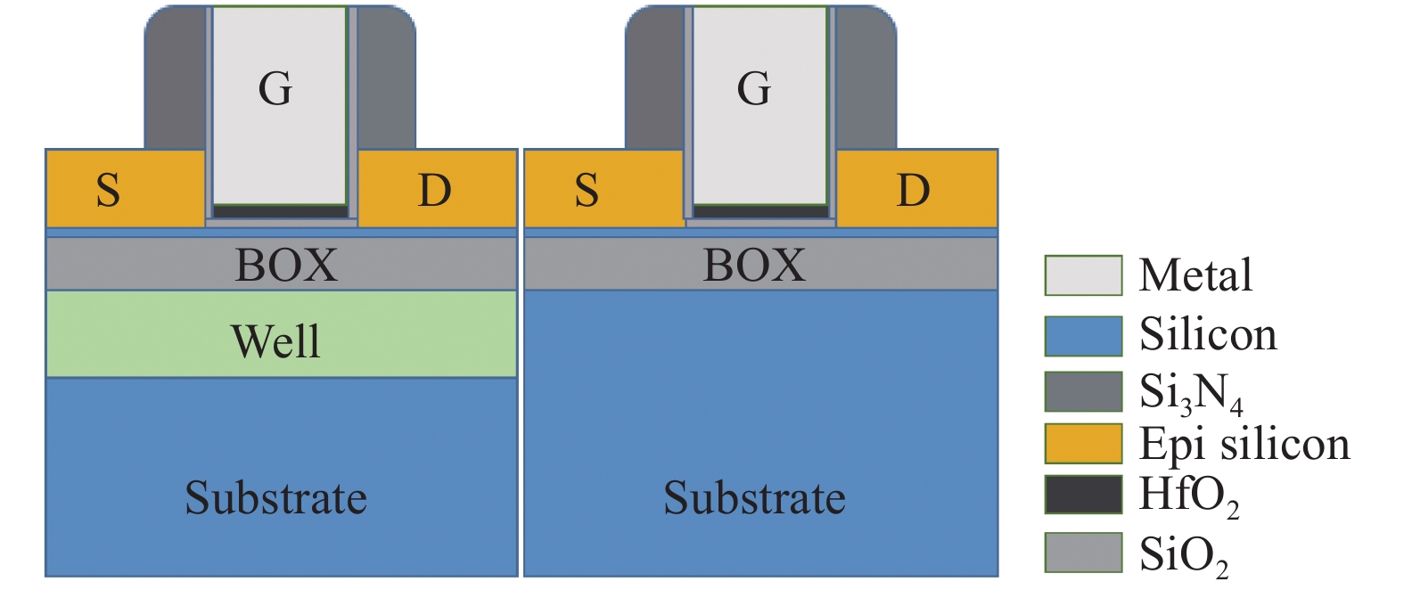
Fig. 1.
(Color online) Schematics of the different studied architectures.
SEMICONDUCTOR DEVICES
Yuqi Ren1, Shizhen Huang1, , Lei Shen2, Xiaoyan Liu2 and Gang Du2
Corresponding author: Shizhen Huang, Email: hs501@qq.com
Abstract: In this work, the impact of well doping and corresponding body bias on UTBB MOSFETs is investigated. The ability of threshold voltage adjustment is evaluated. The results indicate that well doping can change the threshold voltage both of the N and P channel UTBB MOSFETs. The maximum amplitude for a typical 26 nm gate length device is about 100 mV, and these correspond to the cases of devices with an inverse type of high concentration dopant. The body bias adjusts the threshold voltage at a rate of 100–140 mV/V for the UTBB MOSFETs with a well. By optimizing well doping and body biasing, multi-threshold-voltage UTBB MOSFETs can be designed and optimized for lower power application.
Keywords: UTBB MOSFET, well doping, threshold voltage
| [1] |
Hai C H, Han Z S , Zhou X Y ,et al. Study of improved performance of SOI devices and circuits. Chin J Semicond, 2006, 27: 322
|
| [2] |
Cheng K G, Khakifirooz A. Fully depleted SOI (FDSOI) technology. Sci Chin Inf Sci, 2006, 27(6): 061402
|
| [3] |
Yamamoto Y, Makiyama H, Shinohara H, et al. Ultralow-voltage operation of silicon-on-thin-BOX (SOTB) 2Mbit SRAM down to 0.37 V utilizing adaptive back bias. Symposium on VLSI Technology, 2013
|
| [4] |
Li L L, Zhou X J , Yu Z G , et al. Effect of phosphorus ion implantation on back gate effect of partially depleted SOI NMOS under total dose radiation. J Semicond, 2015, 36(1): 014006 doi: 10.1088/1674-4926/36/1/014006
|
| [5] |
Zheng Z J, Yu X, Zhang Y Y, et al. Back-gate modulation in UTB GeOI pMOSFETs with advanced substrate fabrication technique. IEEE Trans Electron Devices, 2018, 65(3): 895 doi: 10.1109/TED.2018.2798407
|
| [6] |
Wu W R, Wu H, Zhang J Y, et al. Carrier mobility enhancement by applying back-gate bias in Ge-on-insulator MOSFETs. IEEE Trans Device Letts, 2018, 39(2): 176 doi: 10.1109/LED.2017.2787023
|
| [7] |
Clerc S, Abouzeid F, Patel D A , et al. Design and performance parameters of an ultra-low voltage, single supply 32 bit processor implemented in 28 nm FDSOI technology. Sixteenth International Symposium on Quality Electronic Design (ISQED), 2015: 366
|
| [8] |
Clerc S. A 0.33 V/–40 °C process/temperature closed-loop compensation SoC embedding all-digital clock multiplier and DC-DC converter exploiting FDSOI 28 nm back-gate biasing. IEEE International Solid-State Circuits Conference Digest of Technical Papers (ISSCC), 2015: 150
|
| [9] |
Wu W K, An X, Tan F, et al. Effects of heavy ion irradiation on ultra-deep-submicron partially-depleted SOI devices. J Semicond, 2015, 36(11): 114004 doi: 10.1088/1674-4926/36/11/114004
|
| [10] |
Noel J P. A simple and efficient concept for setting up multi-VT devices in thin BOX fully-depleted SOI technology. IEEE ESSDERC, 2009: 137
|
| [11] |
Thomas O, Noel J P, Fenouillet-Beranger C, et al. 32 nm and beyond multi-Vt ultra-thin body and BOX FDSOI: From device to circuit. Proceedings of 2010 IEEE International Symposium on Circuits and Systems (ISCAS), 2010: 1703
|
| [12] |
Fenouillet-Beranger C, Perreau P, Denorme S, et al. Impact of a 10 nm ultra-thin BOX(UTBOX) and ground plane on FDSOI devices for 32 nm node and below. Solid-State Electron, 2010, 54: 849 doi: 10.1016/j.sse.2010.04.009
|
| [13] |
Fenouillet-Beranger C, Perreau P, Denorme S, et al, FDSOI devices with thin BOX and ground plane integration for 32 nm node and below. FDSOI devices with thin BOX and ground plane integration for 32 nm node and below. Solid-State Electron, 2009, 53: 730 doi: 10.1016/j.sse.2009.02.009
|
| [14] |
Synopsys, Sentaurus Device User Guide H-2013.03. USA: Synopsys, March 2013
|
| [15] |
Noel J P, Thomas O. Multi-Vt UTBB FDSOI device architectures for low-power CMOS circuit. IEEE Trans Electron Devices, 2011, 58: 2473 doi: 10.1109/TED.2011.2155658
|
| [16] |
Skotnicki T, Monfray S. UTBB FDSOI: Evolution and opportunities. Solid-State Electron, 2016, 125: 63 doi: 10.1016/j.sse.2016.07.003
|
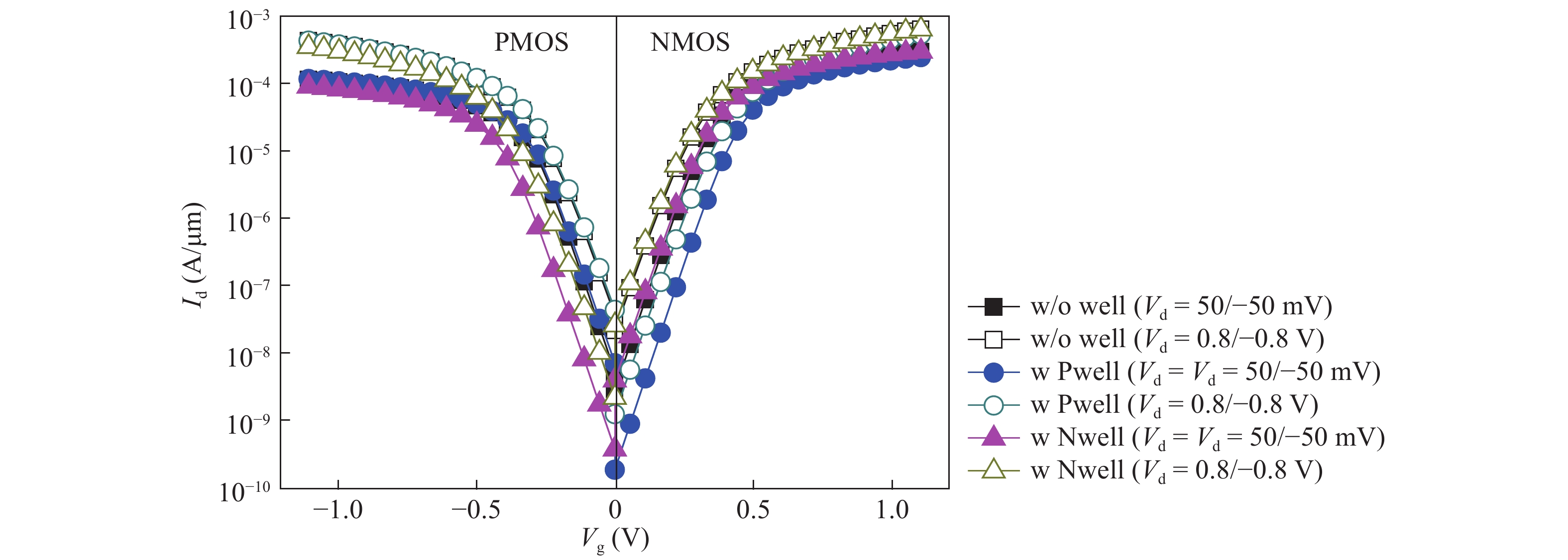
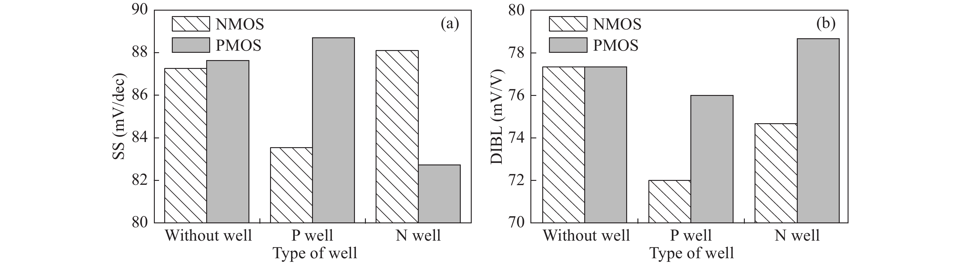
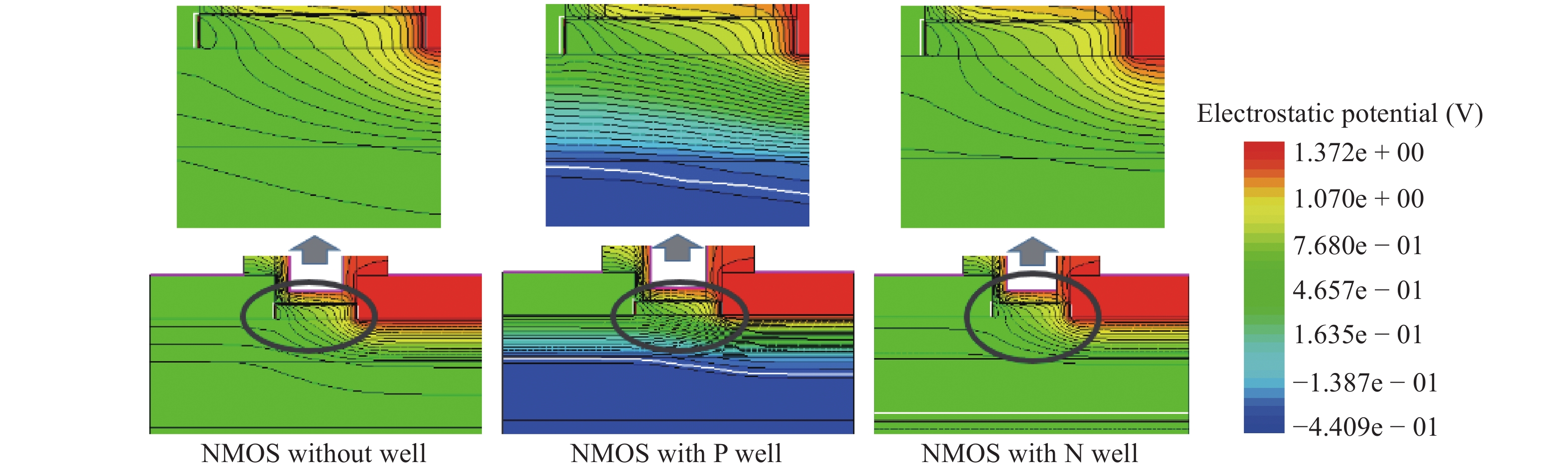
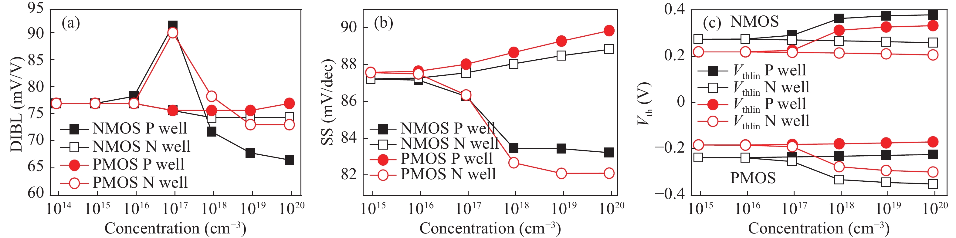
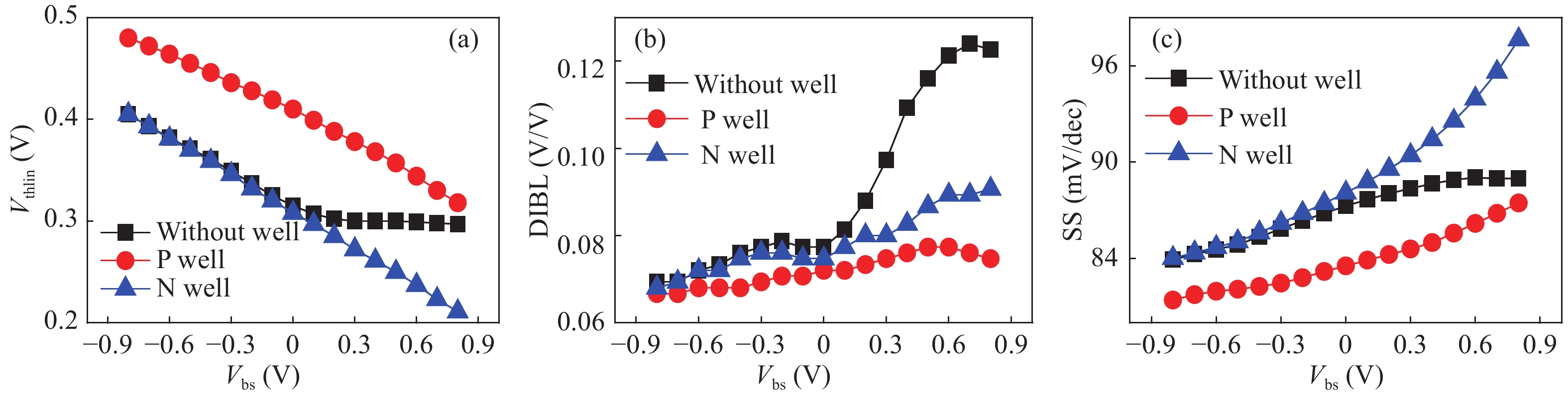
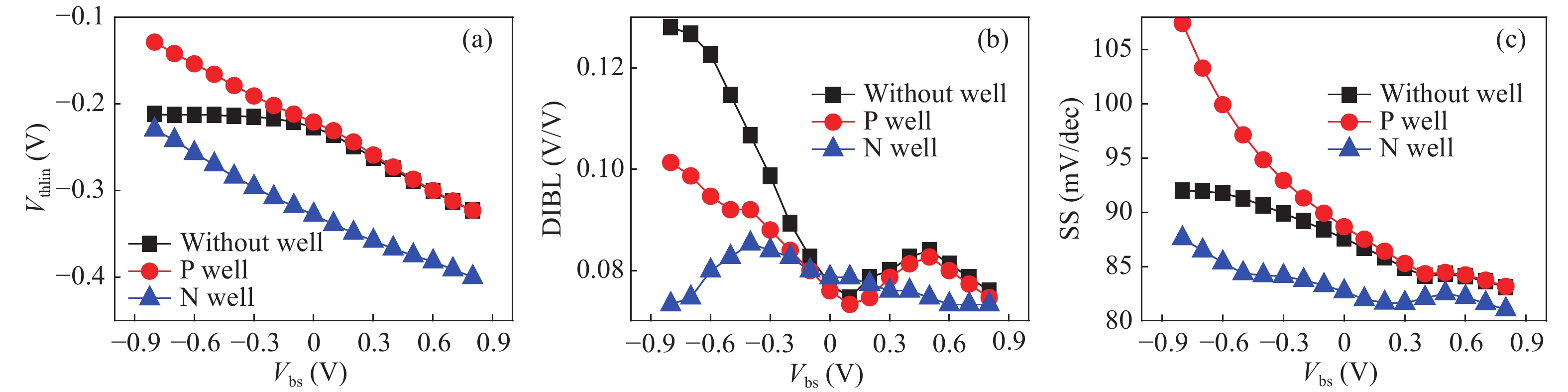
Table 1. The parameters of devices.
| Parameter | PMOS | NMOS |
| Length of gate (nm) | 26 | 26 |
| Silicon film thickness (nm) | 6.5 | 6.5 |
| Effect oxide thickness (nm) | 1.4 | 1.4 |
| Concentration of S/D (1020 cm−3) | 1 | 3 |
| Concentration of channel (1016 cm−3) | 5 | 6 |
| Concentration of substrate (1014 cm−3) | 1 (P) | 1 (P) |
 DownLoad: CSV
Table 2. Threshold voltage shift for the six types of devices.
| Type of device | NMOS w/o well | NMOS with Pwell | NMOS with Nwell | PMOS w/o well | PMOS with Pwell | PMOS with Nwell |
| Vth variation (mV) | 0 | 95 | −7 | 0 | 6 | −107 |
DownLoad: CSV
| [1] |
Hai C H, Han Z S , Zhou X Y ,et al. Study of improved performance of SOI devices and circuits. Chin J Semicond, 2006, 27: 322
|
| [2] |
Cheng K G, Khakifirooz A. Fully depleted SOI (FDSOI) technology. Sci Chin Inf Sci, 2006, 27(6): 061402
|
| [3] |
Yamamoto Y, Makiyama H, Shinohara H, et al. Ultralow-voltage operation of silicon-on-thin-BOX (SOTB) 2Mbit SRAM down to 0.37 V utilizing adaptive back bias. Symposium on VLSI Technology, 2013
|
| [4] |
Li L L, Zhou X J , Yu Z G , et al. Effect of phosphorus ion implantation on back gate effect of partially depleted SOI NMOS under total dose radiation. J Semicond, 2015, 36(1): 014006 doi: 10.1088/1674-4926/36/1/014006
|
| [5] |
Zheng Z J, Yu X, Zhang Y Y, et al. Back-gate modulation in UTB GeOI pMOSFETs with advanced substrate fabrication technique. IEEE Trans Electron Devices, 2018, 65(3): 895 doi: 10.1109/TED.2018.2798407
|
| [6] |
Wu W R, Wu H, Zhang J Y, et al. Carrier mobility enhancement by applying back-gate bias in Ge-on-insulator MOSFETs. IEEE Trans Device Letts, 2018, 39(2): 176 doi: 10.1109/LED.2017.2787023
|
| [7] |
Clerc S, Abouzeid F, Patel D A , et al. Design and performance parameters of an ultra-low voltage, single supply 32 bit processor implemented in 28 nm FDSOI technology. Sixteenth International Symposium on Quality Electronic Design (ISQED), 2015: 366
|
| [8] |
Clerc S. A 0.33 V/–40 °C process/temperature closed-loop compensation SoC embedding all-digital clock multiplier and DC-DC converter exploiting FDSOI 28 nm back-gate biasing. IEEE International Solid-State Circuits Conference Digest of Technical Papers (ISSCC), 2015: 150
|
| [9] |
Wu W K, An X, Tan F, et al. Effects of heavy ion irradiation on ultra-deep-submicron partially-depleted SOI devices. J Semicond, 2015, 36(11): 114004 doi: 10.1088/1674-4926/36/11/114004
|
| [10] |
Noel J P. A simple and efficient concept for setting up multi-VT devices in thin BOX fully-depleted SOI technology. IEEE ESSDERC, 2009: 137
|
| [11] |
Thomas O, Noel J P, Fenouillet-Beranger C, et al. 32 nm and beyond multi-Vt ultra-thin body and BOX FDSOI: From device to circuit. Proceedings of 2010 IEEE International Symposium on Circuits and Systems (ISCAS), 2010: 1703
|
| [12] |
Fenouillet-Beranger C, Perreau P, Denorme S, et al. Impact of a 10 nm ultra-thin BOX(UTBOX) and ground plane on FDSOI devices for 32 nm node and below. Solid-State Electron, 2010, 54: 849 doi: 10.1016/j.sse.2010.04.009
|
| [13] |
Fenouillet-Beranger C, Perreau P, Denorme S, et al, FDSOI devices with thin BOX and ground plane integration for 32 nm node and below. FDSOI devices with thin BOX and ground plane integration for 32 nm node and below. Solid-State Electron, 2009, 53: 730 doi: 10.1016/j.sse.2009.02.009
|
| [14] |
Synopsys, Sentaurus Device User Guide H-2013.03. USA: Synopsys, March 2013
|
| [15] |
Noel J P, Thomas O. Multi-Vt UTBB FDSOI device architectures for low-power CMOS circuit. IEEE Trans Electron Devices, 2011, 58: 2473 doi: 10.1109/TED.2011.2155658
|
| [16] |
Skotnicki T, Monfray S. UTBB FDSOI: Evolution and opportunities. Solid-State Electron, 2016, 125: 63 doi: 10.1016/j.sse.2016.07.003
|


Article views: 4634 Times PDF downloads: 69 Times Cited by: 0 Times
Received: 04 April 2018 Revised: 13 May 2018 Online: Uncorrected proof: 21 June 2018Corrected proof: 01 November 2018Published: 13 December 2018
| Citation: |
Yuqi Ren, Shizhen Huang, Lei Shen, Xiaoyan Liu, Gang Du. Influence of well doping on the performance of UTBB MOSFETs[J]. Journal of Semiconductors, 2018, 39(12): 124005. doi: 10.1088/1674-4926/39/12/124005
****
Y Q Ren, S Z Huang, L Shen, X Y Liu, G Du, Influence of well doping on the performance of UTBB MOSFETs[J]. J. Semicond., 2018, 39(12): 124005. doi: 10.1088/1674-4926/39/12/124005.

|
| [1] |
Hai C H, Han Z S , Zhou X Y ,et al. Study of improved performance of SOI devices and circuits. Chin J Semicond, 2006, 27: 322
|
| [2] |
Cheng K G, Khakifirooz A. Fully depleted SOI (FDSOI) technology. Sci Chin Inf Sci, 2006, 27(6): 061402
|
| [3] |
Yamamoto Y, Makiyama H, Shinohara H, et al. Ultralow-voltage operation of silicon-on-thin-BOX (SOTB) 2Mbit SRAM down to 0.37 V utilizing adaptive back bias. Symposium on VLSI Technology, 2013
|
| [4] |
Li L L, Zhou X J , Yu Z G , et al. Effect of phosphorus ion implantation on back gate effect of partially depleted SOI NMOS under total dose radiation. J Semicond, 2015, 36(1): 014006 doi: 10.1088/1674-4926/36/1/014006
|
| [5] |
Zheng Z J, Yu X, Zhang Y Y, et al. Back-gate modulation in UTB GeOI pMOSFETs with advanced substrate fabrication technique. IEEE Trans Electron Devices, 2018, 65(3): 895 doi: 10.1109/TED.2018.2798407
|
| [6] |
Wu W R, Wu H, Zhang J Y, et al. Carrier mobility enhancement by applying back-gate bias in Ge-on-insulator MOSFETs. IEEE Trans Device Letts, 2018, 39(2): 176 doi: 10.1109/LED.2017.2787023
|
| [7] |
Clerc S, Abouzeid F, Patel D A , et al. Design and performance parameters of an ultra-low voltage, single supply 32 bit processor implemented in 28 nm FDSOI technology. Sixteenth International Symposium on Quality Electronic Design (ISQED), 2015: 366
|
| [8] |
Clerc S. A 0.33 V/–40 °C process/temperature closed-loop compensation SoC embedding all-digital clock multiplier and DC-DC converter exploiting FDSOI 28 nm back-gate biasing. IEEE International Solid-State Circuits Conference Digest of Technical Papers (ISSCC), 2015: 150
|
| [9] |
Wu W K, An X, Tan F, et al. Effects of heavy ion irradiation on ultra-deep-submicron partially-depleted SOI devices. J Semicond, 2015, 36(11): 114004 doi: 10.1088/1674-4926/36/11/114004
|
| [10] |
Noel J P. A simple and efficient concept for setting up multi-VT devices in thin BOX fully-depleted SOI technology. IEEE ESSDERC, 2009: 137
|
| [11] |
Thomas O, Noel J P, Fenouillet-Beranger C, et al. 32 nm and beyond multi-Vt ultra-thin body and BOX FDSOI: From device to circuit. Proceedings of 2010 IEEE International Symposium on Circuits and Systems (ISCAS), 2010: 1703
|
| [12] |
Fenouillet-Beranger C, Perreau P, Denorme S, et al. Impact of a 10 nm ultra-thin BOX(UTBOX) and ground plane on FDSOI devices for 32 nm node and below. Solid-State Electron, 2010, 54: 849 doi: 10.1016/j.sse.2010.04.009
|
| [13] |
Fenouillet-Beranger C, Perreau P, Denorme S, et al, FDSOI devices with thin BOX and ground plane integration for 32 nm node and below. FDSOI devices with thin BOX and ground plane integration for 32 nm node and below. Solid-State Electron, 2009, 53: 730 doi: 10.1016/j.sse.2009.02.009
|
| [14] |
Synopsys, Sentaurus Device User Guide H-2013.03. USA: Synopsys, March 2013
|
| [15] |
Noel J P, Thomas O. Multi-Vt UTBB FDSOI device architectures for low-power CMOS circuit. IEEE Trans Electron Devices, 2011, 58: 2473 doi: 10.1109/TED.2011.2155658
|
| [16] |
Skotnicki T, Monfray S. UTBB FDSOI: Evolution and opportunities. Solid-State Electron, 2016, 125: 63 doi: 10.1016/j.sse.2016.07.003
|

 WeChat ID
Journal of Semiconductors © 2017 All Rights Reserved 京ICP备05085259号-2


