


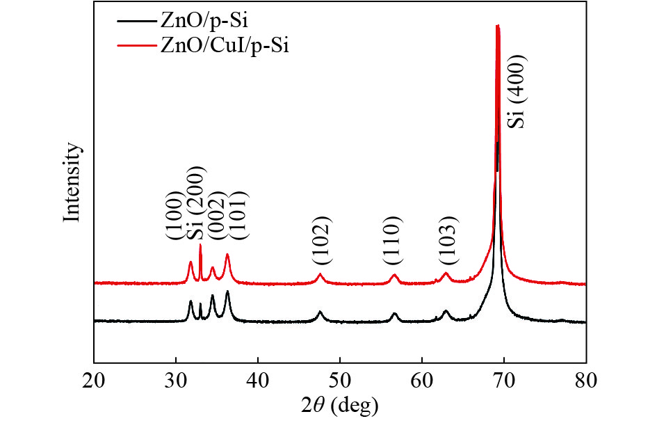
Fig. 1.
(Color online) X-ray diffraction pattern of ZnO/p-Si and ZnO/CuI/p-Si heterojunctions.
SEMICONDUCTOR DEVICES
Chao Xiong, Jin Xiao, Lei Chen, Wenhan Du, Weilong Xu and Dongdong Hou
Corresponding author: Chao Xiong, Email: xiongc@czu.cn
Abstract: The ZnO/Si heterojunction diode can be integrated with the Si process, which has attracted great attention in recent years. However, the large number of interface states at the ZnO/ Si heterojunction interface could adversely affect its optoelectronic properties. Here, n-type ZnO thin film was deposited on p-Si substrate for formation of an n-ZnO/p-Si heterojunction substrate. To passivate the ZnO/Si interface, a thin CuI film interface passivation layer was inserted at the ZnO/p-Si heterojunction interface. Electrical characterization such as I–V and C–V characteristic curves confirmed the significant improvement of the heterojunction properties e.g. enhancement of forward current injection, reduction of reverse current and improvement of the rectification ratio. These results showed that the passivation of interface is critical for ZnO/Si heterojunctions.
Keywords: ZnO/p-Si, heterojunction, CuI, interface states, electrical properties
| [1] |
Ilican S, Gorgun K, Aksoy S, et al. Fabrication of p-Si/n-ZnO:Al heterojunction diode and determination of electrical parameters. J Mol Struct, 2018, 1156(15): 675
|
| [2] |
Sahare P D, Kumar S, Kumar S, et al. n-ZnO/p-Si heterojunction nanodiodes based sensor for monitoring UV radiation. Sens Actuators A, 2018, 279(15): 351
|
| [3] |
Kang J H, Lee K S, Kim E K. Photovoltaic property of n-ZnO/p-Si heterojunctions grown by pulsed laser deposition. Thin Solid Films, 2018, 658(31): 22
|
| [4] |
Paul S, Sultana J, Bhattacharyya A, et al. Investigation of the comparative photovoltaic performance of n-ZnO nanowire/p-Si and n-ZnO nanowire/p-CuO heterojunctions grown by chemical bath deposition method. Optik, 2018, 164: 745 doi: 10.1016/j.ijleo.2018.03.076
|
| [5] |
Labar R, Kundu T K. Barrier inhomogeneities in n-ZnO/p-Si heterojunctions fabricated with ZnO nanorods. J Electron Mater, 2018, 47(7): 3628 doi: 10.1007/s11664-018-6209-6
|
| [6] |
Lee J Y, Choi Y S, Kim J H, et al. Optimizing n-ZnO/p-Si heterojunctions for photodiode applications. Thin Solid Films, 2005, 403/404: 553
|
| [7] |
Dellis S, Pliatsikas N, Kalfagiannis N, et al. Broadband luminescence in defect-engineered electrochemically produced porous Si/ZnO nanostructures. Sci Rep, 2018, 8: 6988 doi: 10.1038/s41598-018-24684-6
|
| [8] |
Mridha S, Basak D. Ultraviolet and visible photoresponse properties of n-ZnO/p-Si heterojunction. J Appl Phys, 2007, 110(8): 083102
|
| [9] |
Mridha S, Dutta M, Basak D. Photoresponse of n-ZnO/p-Si heterojunction towards ultraviolet/visible lights: thickness dependent behavior. J Mater Sci–Mater Electron, 2009, 20: S376 doi: 10.1007/s10854-008-9628-y
|
| [10] |
Zhang C T, Guo Y, Mei Z X, et al. Visible-blind ultraviolet photodetector based on double heterojunction of n-ZnO/insulator-MgO/p-Si. Appl Phys Lett, 2009, 94(11): 113508 doi: 10.1063/1.3103272
|
| [11] |
Lu Y, Huang J, Li B, et al. A boron and gallium co-doped ZnO intermediate layer for ZnO/Si heterojunction diodes. Appl Surf Sci, 2018, 428(15): 61
|
| [12] |
Wenas W W, Riyadi S. Carrier transport in high-efficiency ZnO/SiO2/Si solar cells. Sol Energy Mater Sol Cells, 2006, 90: 3261 doi: 10.1016/j.solmat.2006.06.026
|
| [13] |
Ghosh R, Basak D. Electrical and ultraviolet photoresponse properties of quasialigned ZnO nanowires/p-Si heterojunction. Appl Phys Lett, 2007, 90: 243106 doi: 10.1063/1.2748333
|
| [14] |
Baltakesmez A, Yenisoy A, Tüzemen S, et al. Effects of gold nanoparticles on the growth of ZnO thin films and p-Si/ZnO heterostructures. Mater Sci Semicond Process, 2018, 74: 249 doi: 10.1016/j.mssp.2017.10.037
|
| [15] |
Mridha S, Basak D. Ultraviolet and visible photoresponse properties of n-ZnO/p-Si heterojunction. J Appl Phys, 2007, 101(8): 083102 doi: 10.1063/1.2724808
|
| [16] |
Breivik T H, Diplas S, Ulyashin A G, et al. Nano-structural properties of ZnO films for Si based heterojunction solar cells. Thin Solid Films, 2007, 515: 8479 doi: 10.1016/j.tsf.2007.03.095
|
| [17] |
Zhang W Y, Zhong S, Sun L J, et al. Dependence of photovoltaic property of ZnO/Si heterojunction solar cell on thickness of ZnO films. Chin Phys Lett, 2008, 25(5): 1829 doi: 10.1088/0256-307X/25/5/083
|
| [18] |
Liu Y J, Yu H Z. Molecular passivation of mercury-silicon (p-type) diode junctions: alkylation, oxidation, and alkylsilation. J Phys Chem B, 2003, 107: 7803 doi: 10.1021/jp034791d
|
| [19] |
Chattopadhyay P. Capacitance technique for the determination of interface state density of metal-semiconductor contact. Solid-State Electron, 1996, 39(10): 1491 doi: 10.1016/0038-1101(96)00058-5
|
| [20] |
Santosh P, Kal S. A simple approach to the capacitance technique for determination of interface state density of a metal-semiconductor contact. Solid-State Electron, 1998, 42(6): 943 doi: 10.1016/S0038-1101(97)00267-0
|
| [21] |
Iimori H, Yamane S, Kitamura T, et al. High photovoltage generation at minority-carrier controlled n-Si/p-CuI heterojunction with morphologically soft CuI. J Phys Chem C, 2008, 112: 11585
|
| [22] |
Donnelly J P, Milnes A G. The Capacitance of p-n heterojunctions including the effects of interface states. IEEE Trans Electron Devices, 1967, 14(2): 63 doi: 10.1109/T-ED.1967.15900
|
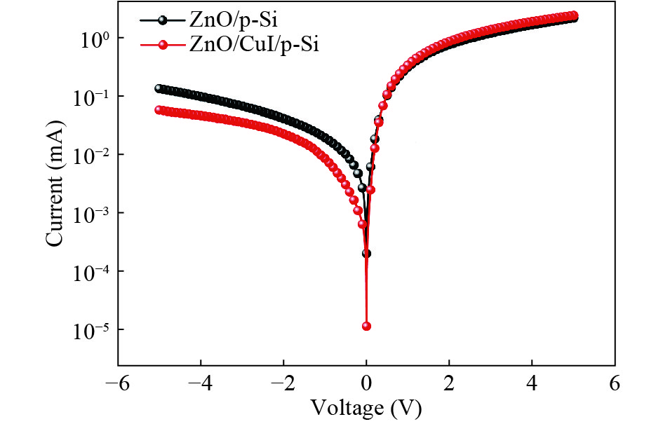
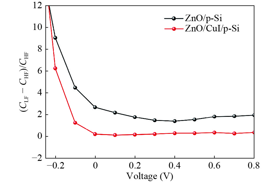
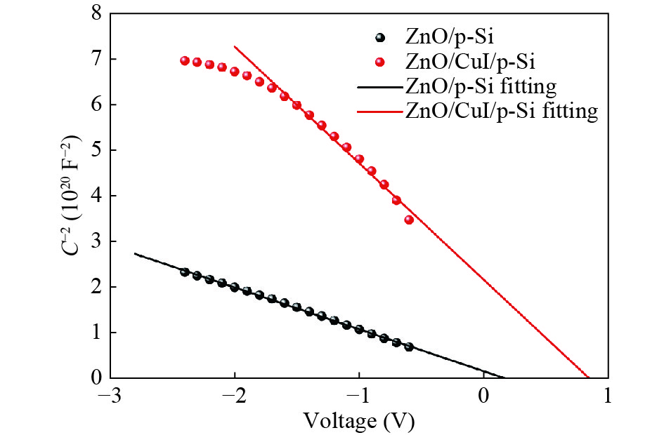
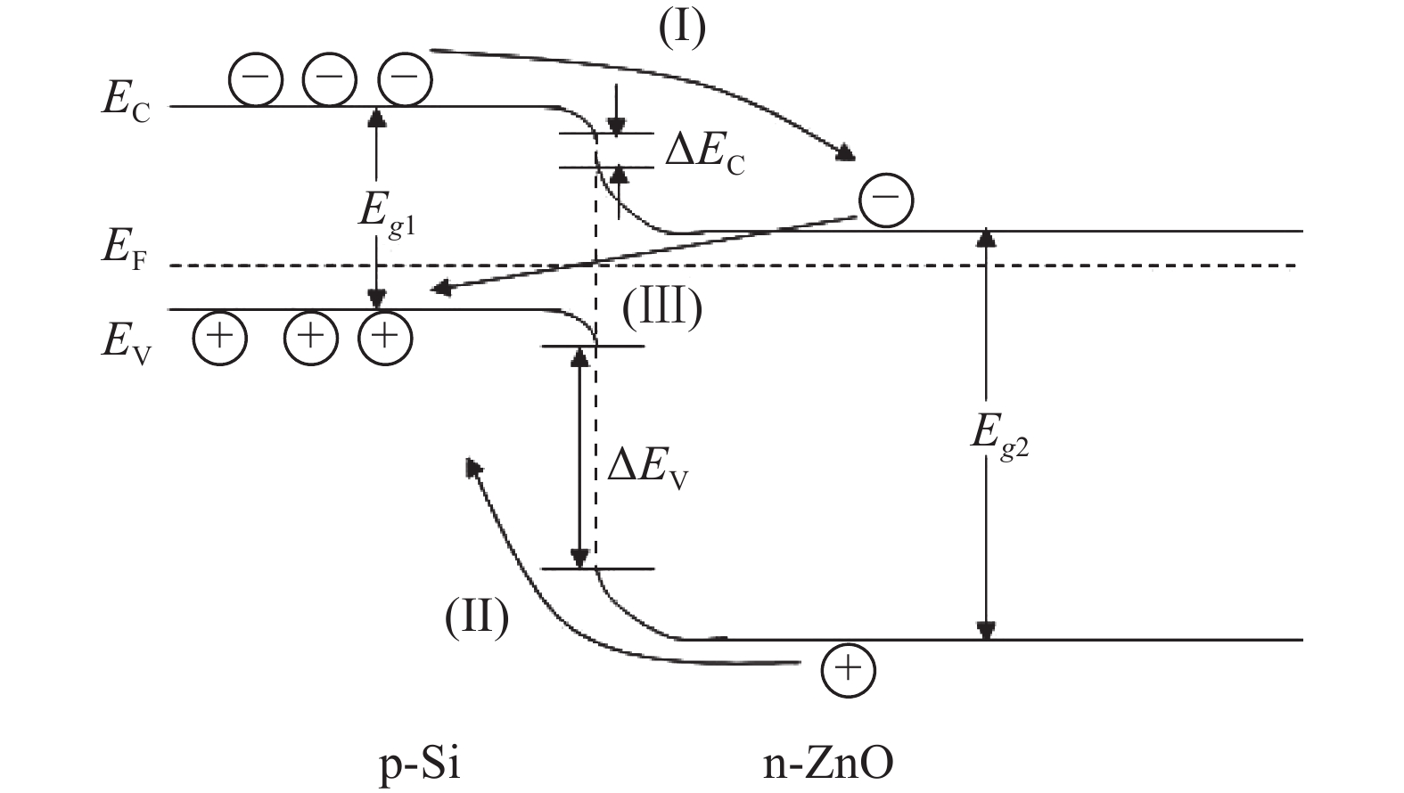
Table 1. Process for preparation of CuI films by SILAR.
| Chemical component | CuSO4·5H2O + Na2S2O3 | Deionized water (H2O) | KI | Deionized water (H2O) |
| Concentration | 5 × 0.1 mol/dm3 + 2 × 0.1 mol/dm3 | With electrical resistivity of 18 MΩ·cm | 0.025 mol/dm3 | With electrical resistivity of 18 MΩ·cm |
| PH | ~5 | 7 | ~6 | 7 |
| Specific reaction |


|
Rinsing off the less absorbed Cu+ |


|
Rinsing off the less absorbed Cu+ |
| Soaking time | 5 | 5 | 20 | 5 |
 DownLoad: CSV
| [1] |
Ilican S, Gorgun K, Aksoy S, et al. Fabrication of p-Si/n-ZnO:Al heterojunction diode and determination of electrical parameters. J Mol Struct, 2018, 1156(15): 675
|
| [2] |
Sahare P D, Kumar S, Kumar S, et al. n-ZnO/p-Si heterojunction nanodiodes based sensor for monitoring UV radiation. Sens Actuators A, 2018, 279(15): 351
|
| [3] |
Kang J H, Lee K S, Kim E K. Photovoltaic property of n-ZnO/p-Si heterojunctions grown by pulsed laser deposition. Thin Solid Films, 2018, 658(31): 22
|
| [4] |
Paul S, Sultana J, Bhattacharyya A, et al. Investigation of the comparative photovoltaic performance of n-ZnO nanowire/p-Si and n-ZnO nanowire/p-CuO heterojunctions grown by chemical bath deposition method. Optik, 2018, 164: 745 doi: 10.1016/j.ijleo.2018.03.076
|
| [5] |
Labar R, Kundu T K. Barrier inhomogeneities in n-ZnO/p-Si heterojunctions fabricated with ZnO nanorods. J Electron Mater, 2018, 47(7): 3628 doi: 10.1007/s11664-018-6209-6
|
| [6] |
Lee J Y, Choi Y S, Kim J H, et al. Optimizing n-ZnO/p-Si heterojunctions for photodiode applications. Thin Solid Films, 2005, 403/404: 553
|
| [7] |
Dellis S, Pliatsikas N, Kalfagiannis N, et al. Broadband luminescence in defect-engineered electrochemically produced porous Si/ZnO nanostructures. Sci Rep, 2018, 8: 6988 doi: 10.1038/s41598-018-24684-6
|
| [8] |
Mridha S, Basak D. Ultraviolet and visible photoresponse properties of n-ZnO/p-Si heterojunction. J Appl Phys, 2007, 110(8): 083102
|
| [9] |
Mridha S, Dutta M, Basak D. Photoresponse of n-ZnO/p-Si heterojunction towards ultraviolet/visible lights: thickness dependent behavior. J Mater Sci–Mater Electron, 2009, 20: S376 doi: 10.1007/s10854-008-9628-y
|
| [10] |
Zhang C T, Guo Y, Mei Z X, et al. Visible-blind ultraviolet photodetector based on double heterojunction of n-ZnO/insulator-MgO/p-Si. Appl Phys Lett, 2009, 94(11): 113508 doi: 10.1063/1.3103272
|
| [11] |
Lu Y, Huang J, Li B, et al. A boron and gallium co-doped ZnO intermediate layer for ZnO/Si heterojunction diodes. Appl Surf Sci, 2018, 428(15): 61
|
| [12] |
Wenas W W, Riyadi S. Carrier transport in high-efficiency ZnO/SiO2/Si solar cells. Sol Energy Mater Sol Cells, 2006, 90: 3261 doi: 10.1016/j.solmat.2006.06.026
|
| [13] |
Ghosh R, Basak D. Electrical and ultraviolet photoresponse properties of quasialigned ZnO nanowires/p-Si heterojunction. Appl Phys Lett, 2007, 90: 243106 doi: 10.1063/1.2748333
|
| [14] |
Baltakesmez A, Yenisoy A, Tüzemen S, et al. Effects of gold nanoparticles on the growth of ZnO thin films and p-Si/ZnO heterostructures. Mater Sci Semicond Process, 2018, 74: 249 doi: 10.1016/j.mssp.2017.10.037
|
| [15] |
Mridha S, Basak D. Ultraviolet and visible photoresponse properties of n-ZnO/p-Si heterojunction. J Appl Phys, 2007, 101(8): 083102 doi: 10.1063/1.2724808
|
| [16] |
Breivik T H, Diplas S, Ulyashin A G, et al. Nano-structural properties of ZnO films for Si based heterojunction solar cells. Thin Solid Films, 2007, 515: 8479 doi: 10.1016/j.tsf.2007.03.095
|
| [17] |
Zhang W Y, Zhong S, Sun L J, et al. Dependence of photovoltaic property of ZnO/Si heterojunction solar cell on thickness of ZnO films. Chin Phys Lett, 2008, 25(5): 1829 doi: 10.1088/0256-307X/25/5/083
|
| [18] |
Liu Y J, Yu H Z. Molecular passivation of mercury-silicon (p-type) diode junctions: alkylation, oxidation, and alkylsilation. J Phys Chem B, 2003, 107: 7803 doi: 10.1021/jp034791d
|
| [19] |
Chattopadhyay P. Capacitance technique for the determination of interface state density of metal-semiconductor contact. Solid-State Electron, 1996, 39(10): 1491 doi: 10.1016/0038-1101(96)00058-5
|
| [20] |
Santosh P, Kal S. A simple approach to the capacitance technique for determination of interface state density of a metal-semiconductor contact. Solid-State Electron, 1998, 42(6): 943 doi: 10.1016/S0038-1101(97)00267-0
|
| [21] |
Iimori H, Yamane S, Kitamura T, et al. High photovoltage generation at minority-carrier controlled n-Si/p-CuI heterojunction with morphologically soft CuI. J Phys Chem C, 2008, 112: 11585
|
| [22] |
Donnelly J P, Milnes A G. The Capacitance of p-n heterojunctions including the effects of interface states. IEEE Trans Electron Devices, 1967, 14(2): 63 doi: 10.1109/T-ED.1967.15900
|


Article views: 4158 Times PDF downloads: 57 Times Cited by: 0 Times
Received: 31 July 2018 Revised: 29 September 2018 Online: Accepted Manuscript: 12 November 2018Uncorrected proof: 12 November 2018Published: 13 December 2018
| Citation: |
Chao Xiong, Jin Xiao, Lei Chen, Wenhan Du, Weilong Xu, Dongdong Hou. Interfacial passivation of n-ZnO/p-Si heterojunction by CuI thin layer[J]. Journal of Semiconductors, 2018, 39(12): 124013. doi: 10.1088/1674-4926/39/12/124013
****
C Xiong, J Xiao, L Chen, W H Du, W L Xu, D D Hou, Interfacial passivation of n-ZnO/p-Si heterojunction by CuI thin layer[J]. J. Semicond., 2018, 39(12): 124013. doi: 10.1088/1674-4926/39/12/124013.

|
| [1] |
Ilican S, Gorgun K, Aksoy S, et al. Fabrication of p-Si/n-ZnO:Al heterojunction diode and determination of electrical parameters. J Mol Struct, 2018, 1156(15): 675
|
| [2] |
Sahare P D, Kumar S, Kumar S, et al. n-ZnO/p-Si heterojunction nanodiodes based sensor for monitoring UV radiation. Sens Actuators A, 2018, 279(15): 351
|
| [3] |
Kang J H, Lee K S, Kim E K. Photovoltaic property of n-ZnO/p-Si heterojunctions grown by pulsed laser deposition. Thin Solid Films, 2018, 658(31): 22
|
| [4] |
Paul S, Sultana J, Bhattacharyya A, et al. Investigation of the comparative photovoltaic performance of n-ZnO nanowire/p-Si and n-ZnO nanowire/p-CuO heterojunctions grown by chemical bath deposition method. Optik, 2018, 164: 745 doi: 10.1016/j.ijleo.2018.03.076
|
| [5] |
Labar R, Kundu T K. Barrier inhomogeneities in n-ZnO/p-Si heterojunctions fabricated with ZnO nanorods. J Electron Mater, 2018, 47(7): 3628 doi: 10.1007/s11664-018-6209-6
|
| [6] |
Lee J Y, Choi Y S, Kim J H, et al. Optimizing n-ZnO/p-Si heterojunctions for photodiode applications. Thin Solid Films, 2005, 403/404: 553
|
| [7] |
Dellis S, Pliatsikas N, Kalfagiannis N, et al. Broadband luminescence in defect-engineered electrochemically produced porous Si/ZnO nanostructures. Sci Rep, 2018, 8: 6988 doi: 10.1038/s41598-018-24684-6
|
| [8] |
Mridha S, Basak D. Ultraviolet and visible photoresponse properties of n-ZnO/p-Si heterojunction. J Appl Phys, 2007, 110(8): 083102
|
| [9] |
Mridha S, Dutta M, Basak D. Photoresponse of n-ZnO/p-Si heterojunction towards ultraviolet/visible lights: thickness dependent behavior. J Mater Sci–Mater Electron, 2009, 20: S376 doi: 10.1007/s10854-008-9628-y
|
| [10] |
Zhang C T, Guo Y, Mei Z X, et al. Visible-blind ultraviolet photodetector based on double heterojunction of n-ZnO/insulator-MgO/p-Si. Appl Phys Lett, 2009, 94(11): 113508 doi: 10.1063/1.3103272
|
| [11] |
Lu Y, Huang J, Li B, et al. A boron and gallium co-doped ZnO intermediate layer for ZnO/Si heterojunction diodes. Appl Surf Sci, 2018, 428(15): 61
|
| [12] |
Wenas W W, Riyadi S. Carrier transport in high-efficiency ZnO/SiO2/Si solar cells. Sol Energy Mater Sol Cells, 2006, 90: 3261 doi: 10.1016/j.solmat.2006.06.026
|
| [13] |
Ghosh R, Basak D. Electrical and ultraviolet photoresponse properties of quasialigned ZnO nanowires/p-Si heterojunction. Appl Phys Lett, 2007, 90: 243106 doi: 10.1063/1.2748333
|
| [14] |
Baltakesmez A, Yenisoy A, Tüzemen S, et al. Effects of gold nanoparticles on the growth of ZnO thin films and p-Si/ZnO heterostructures. Mater Sci Semicond Process, 2018, 74: 249 doi: 10.1016/j.mssp.2017.10.037
|
| [15] |
Mridha S, Basak D. Ultraviolet and visible photoresponse properties of n-ZnO/p-Si heterojunction. J Appl Phys, 2007, 101(8): 083102 doi: 10.1063/1.2724808
|
| [16] |
Breivik T H, Diplas S, Ulyashin A G, et al. Nano-structural properties of ZnO films for Si based heterojunction solar cells. Thin Solid Films, 2007, 515: 8479 doi: 10.1016/j.tsf.2007.03.095
|
| [17] |
Zhang W Y, Zhong S, Sun L J, et al. Dependence of photovoltaic property of ZnO/Si heterojunction solar cell on thickness of ZnO films. Chin Phys Lett, 2008, 25(5): 1829 doi: 10.1088/0256-307X/25/5/083
|
| [18] |
Liu Y J, Yu H Z. Molecular passivation of mercury-silicon (p-type) diode junctions: alkylation, oxidation, and alkylsilation. J Phys Chem B, 2003, 107: 7803 doi: 10.1021/jp034791d
|
| [19] |
Chattopadhyay P. Capacitance technique for the determination of interface state density of metal-semiconductor contact. Solid-State Electron, 1996, 39(10): 1491 doi: 10.1016/0038-1101(96)00058-5
|
| [20] |
Santosh P, Kal S. A simple approach to the capacitance technique for determination of interface state density of a metal-semiconductor contact. Solid-State Electron, 1998, 42(6): 943 doi: 10.1016/S0038-1101(97)00267-0
|
| [21] |
Iimori H, Yamane S, Kitamura T, et al. High photovoltage generation at minority-carrier controlled n-Si/p-CuI heterojunction with morphologically soft CuI. J Phys Chem C, 2008, 112: 11585
|
| [22] |
Donnelly J P, Milnes A G. The Capacitance of p-n heterojunctions including the effects of interface states. IEEE Trans Electron Devices, 1967, 14(2): 63 doi: 10.1109/T-ED.1967.15900
|

 WeChat ID
Journal of Semiconductors © 2017 All Rights Reserved 京ICP备05085259号-2


