


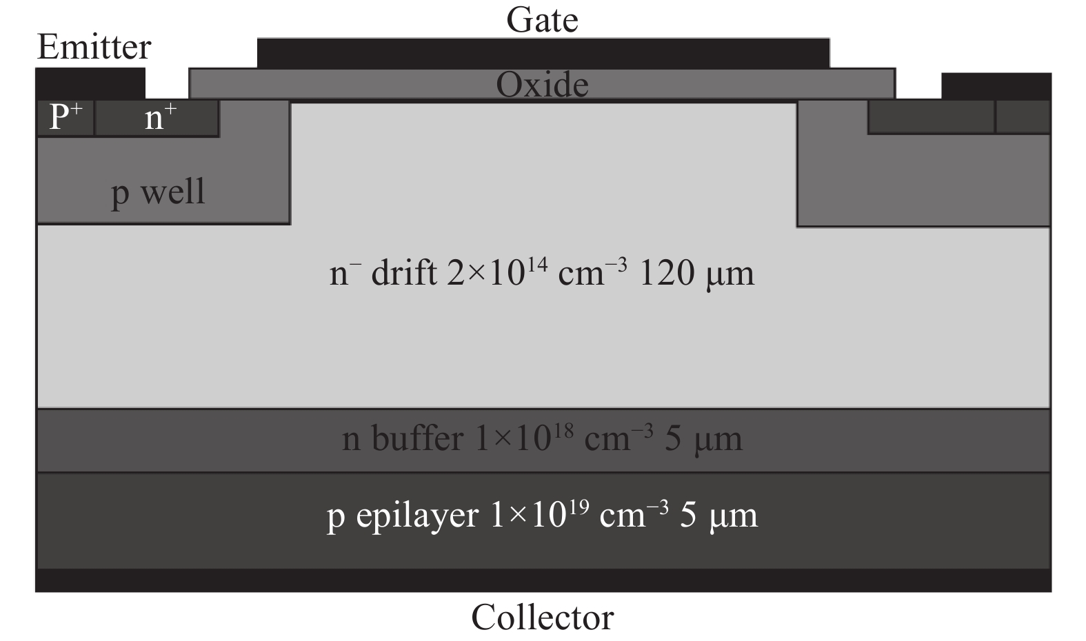
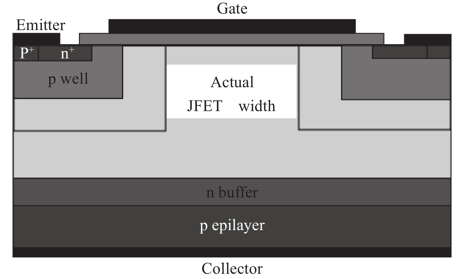
Fig. 1.
Schematic cross-sectional structure of the fabricated n-channel 4H-SiC IGBT.
SEMICONDUCTOR DEVICES
Xiaolei Yang, Yonghong Tao, Tongtong Yang, Runhua Huang and Bai Song
Corresponding author: Xiaolei Yang, 1046990531@qq.com
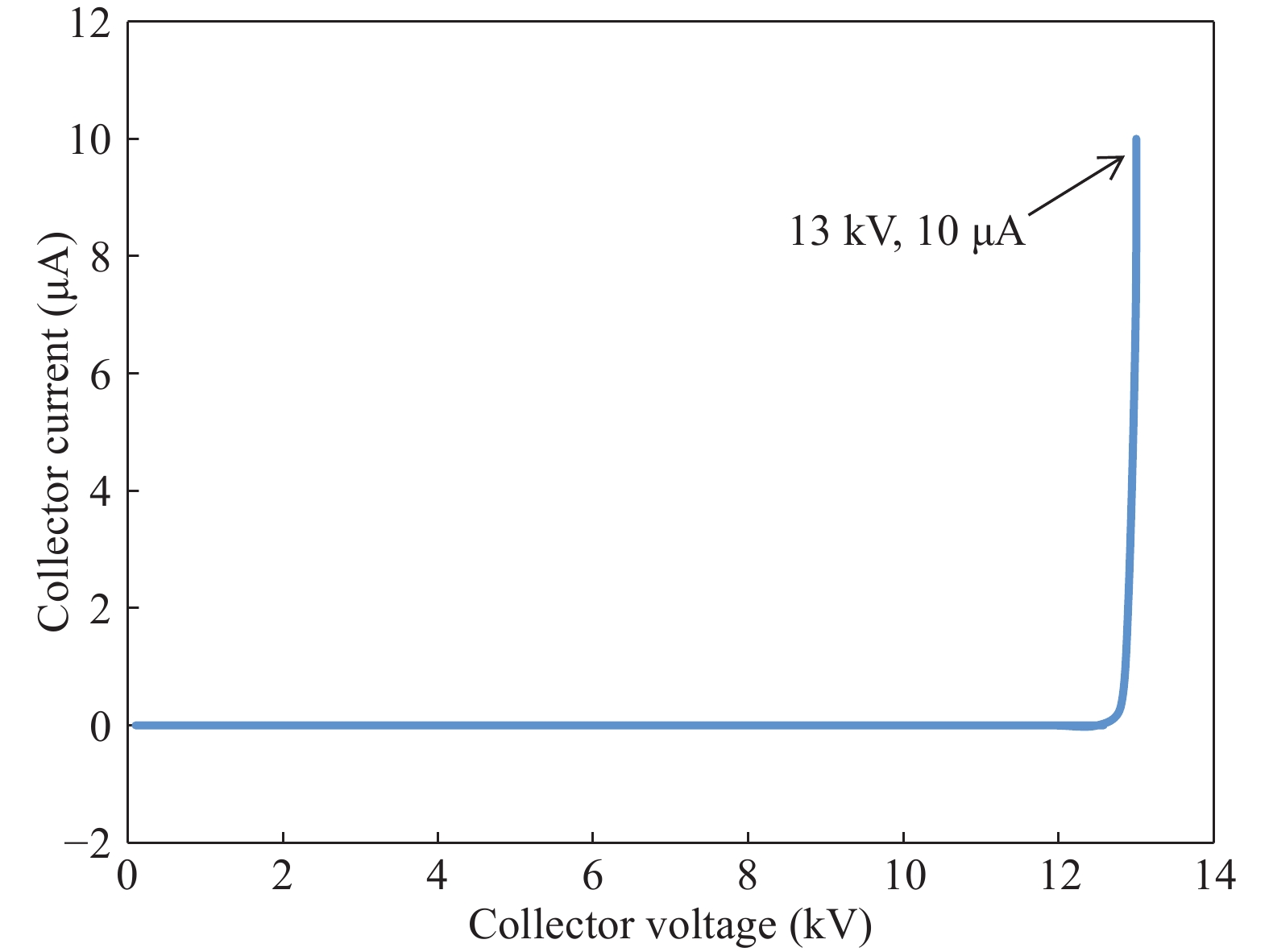
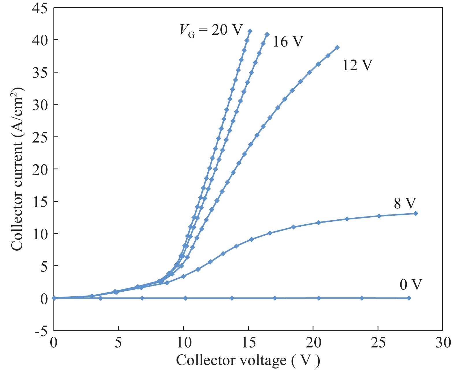
Abstract: Owing to the conductivity modulation of silicon carbide (SiC) bipolar devices, n-channel insulated gate bipolar transistors (n-IGBTs) have a significant advantage over metal oxide semiconductor field effect transistors (MOSFETs) in ultra high voltage (UHV) applications. In this paper, backside grinding and laser annealing process were carried out to fabricate 4H-SiC n-IGBTs. The thickness of a drift layer was 120 μm, which was designed for a blocking voltage of 13 kV. The n-IGBTs carried a collector current density of 24 A/cm2 at a power dissipation of 300 W/cm2 when the gate voltage was 20 V, with a differential specific on-resistance of 140 mΩ·cm2.
Keywords: 4H-SiC, n-channel, IGBT, ultra high voltage
| [1] |
Watanabe N, Yoshimoto H, Shima A, et al. 6.5 kV n-channel 4H-SiC IGBT with low switching loss achieved by extremely thin drift layer. Mater Sci Forum, 2016, 858: 939
|
| [2] |
Baliga B J. Fundamentals of power semiconductor devices. Springer Science & Business Media, 2008
|
| [3] |
Tamaki T, Walden G G, Sui Y, et al. Cooper, et al. ON-state and switching performance of high-voltage 15–20 kV 4H-SiC DMOSFETs and IGBTs. Proc ICSCRM, 2007: 14
|
| [4] |
Zhang N, Rao Y, Xu N, et al. Characterization of 4H-SiC bipolar junction transistor at high temperatures. Mater Sci Forum, 2014, 778–780: 1013 doi: 10.4028/www.scientific.net/MSF.778-780
|
| [5] |
Katakami S, Fujisawa H, Takenaka K, et al. Fabrication of a P-channel SiC-IGBT with high channel mobility. Mater Sci Forum, 2013, 740: 958
|
| [6] |
Ryu S, Capell C, Jonas C, et al. 15 kV IGBTs in 4H-SiC. Mater Sci Forum, 2013, 740: 954
|
| [7] |
Wang X K, Cooper J A. High-voltage n-channel IGBTs on free-standing 4H-SiC epilayers. IEEE Trans Electron Devices, 2010, 57: 2 doi: 10.1109/TED.2010.2048092
|
| [8] |
Ryu S, Capell C, Van Brunt E, et al. Ultra high voltage MOS controlled 4H-SiC power switching devices. Semicond Sci Technol, 2015, 30: 730
|
| [9] |
Grieb M, Noborio M, Peters D, et al. Electrical characterization of MOS structures with deposited oxides annealed in N2O or NO. Mater Sci Forum, 2009, 615-617: 521 doi: 10.4028/www.scientific.net/MSF.615-617
|
| [10] |
Yan H L, Jia R X, Tang X Y, et al. Effect of reoxidation annealing process on the SiO2/SiC interface characteristics. J Semicond, 2014, 35(6): 066001 doi: 10.1088/1674-4926/35/6/066001
|
| [11] |
Zhang E X, Zhang C X, Fleetwod D M, et al. Bias-temperature instabilities in 4H-SiC metal–oxide–semiconductor capacitors. IEEE Trans Device Mater Reliab, 2012, 12(2): 391 doi: 10.1109/TDMR.2012.2188404
|
| [12] |
Yang T T, Bai S, Huang R H. Optimization of junction termination extension for ultrahigh voltage 4H-SiC planar power devices. J Semicond, 2017, 38(4): 044004 doi: 10.1088/1674-4926/38/4/044004
|
| [13] |
Huang R H, Tao Y H, Chen G. Simulation, fabrication and characterization of 6500 V 4H-SiC JBS diode. Adv Mater Res, 2014, 737: 846
|
| [14] |
Elahipanah H, Salemi A, Zetterling C M, et al. Modification of etched junction termination extension for the high voltage 4H-SiC power devices. Mater Sci Forum, 2015, 858: 978
|
| [15] |
Okamoto D, Sometani M, Harada S, et al. Improved channel mobility in 4H-SiC MOSFETs by boron passivation. IEEE Electron Device Lett, 2014, 35: 12 doi: 10.1109/LED.2013.2291394
|
| [16] |
Ryu S, Capell C, Jonas C, et al. An analysis of forward conduction characteristics of ultra high voltage 4H-SiC N-IGBTs. Mater Sci Forum, 2016, 858: 945 doi: 10.4028/www.scientific.net/MSF.858
|


Article views: 6697 Times PDF downloads: 257 Times Cited by: 0 Times
Received: 07 September 2017 Revised: 07 December 2017 Online: Accepted Manuscript: 10 January 2018Uncorrected proof: 24 January 2018Published: 01 March 2018
| Citation: |
Xiaolei Yang, Yonghong Tao, Tongtong Yang, Runhua Huang, Bai Song. Fabrication of 4H-SiC n-channel IGBTs with ultra high blocking voltage[J]. Journal of Semiconductors, 2018, 39(3): 034005. doi: 10.1088/1674-4926/39/3/034005
****
X L Yang, Y H Tao, T T Yang, R H Huang, B Song. Fabrication of 4H-SiC n-channel IGBTs with ultra high blocking voltage[J]. J. Semicond., 2018, 39(3): 034005. doi: 10.1088/1674-4926/39/3/034005.

|
| [1] |
Watanabe N, Yoshimoto H, Shima A, et al. 6.5 kV n-channel 4H-SiC IGBT with low switching loss achieved by extremely thin drift layer. Mater Sci Forum, 2016, 858: 939
|
| [2] |
Baliga B J. Fundamentals of power semiconductor devices. Springer Science & Business Media, 2008
|
| [3] |
Tamaki T, Walden G G, Sui Y, et al. Cooper, et al. ON-state and switching performance of high-voltage 15–20 kV 4H-SiC DMOSFETs and IGBTs. Proc ICSCRM, 2007: 14
|
| [4] |
Zhang N, Rao Y, Xu N, et al. Characterization of 4H-SiC bipolar junction transistor at high temperatures. Mater Sci Forum, 2014, 778–780: 1013 doi: 10.4028/www.scientific.net/MSF.778-780
|
| [5] |
Katakami S, Fujisawa H, Takenaka K, et al. Fabrication of a P-channel SiC-IGBT with high channel mobility. Mater Sci Forum, 2013, 740: 958
|
| [6] |
Ryu S, Capell C, Jonas C, et al. 15 kV IGBTs in 4H-SiC. Mater Sci Forum, 2013, 740: 954
|
| [7] |
Wang X K, Cooper J A. High-voltage n-channel IGBTs on free-standing 4H-SiC epilayers. IEEE Trans Electron Devices, 2010, 57: 2 doi: 10.1109/TED.2010.2048092
|
| [8] |
Ryu S, Capell C, Van Brunt E, et al. Ultra high voltage MOS controlled 4H-SiC power switching devices. Semicond Sci Technol, 2015, 30: 730
|
| [9] |
Grieb M, Noborio M, Peters D, et al. Electrical characterization of MOS structures with deposited oxides annealed in N2O or NO. Mater Sci Forum, 2009, 615-617: 521 doi: 10.4028/www.scientific.net/MSF.615-617
|
| [10] |
Yan H L, Jia R X, Tang X Y, et al. Effect of reoxidation annealing process on the SiO2/SiC interface characteristics. J Semicond, 2014, 35(6): 066001 doi: 10.1088/1674-4926/35/6/066001
|
| [11] |
Zhang E X, Zhang C X, Fleetwod D M, et al. Bias-temperature instabilities in 4H-SiC metal–oxide–semiconductor capacitors. IEEE Trans Device Mater Reliab, 2012, 12(2): 391 doi: 10.1109/TDMR.2012.2188404
|
| [12] |
Yang T T, Bai S, Huang R H. Optimization of junction termination extension for ultrahigh voltage 4H-SiC planar power devices. J Semicond, 2017, 38(4): 044004 doi: 10.1088/1674-4926/38/4/044004
|
| [13] |
Huang R H, Tao Y H, Chen G. Simulation, fabrication and characterization of 6500 V 4H-SiC JBS diode. Adv Mater Res, 2014, 737: 846
|
| [14] |
Elahipanah H, Salemi A, Zetterling C M, et al. Modification of etched junction termination extension for the high voltage 4H-SiC power devices. Mater Sci Forum, 2015, 858: 978
|
| [15] |
Okamoto D, Sometani M, Harada S, et al. Improved channel mobility in 4H-SiC MOSFETs by boron passivation. IEEE Electron Device Lett, 2014, 35: 12 doi: 10.1109/LED.2013.2291394
|
| [16] |
Ryu S, Capell C, Jonas C, et al. An analysis of forward conduction characteristics of ultra high voltage 4H-SiC N-IGBTs. Mater Sci Forum, 2016, 858: 945 doi: 10.4028/www.scientific.net/MSF.858
|

 WeChat ID
Journal of Semiconductors © 2017 All Rights Reserved 京ICP备05085259号-2

 DownLoad:

