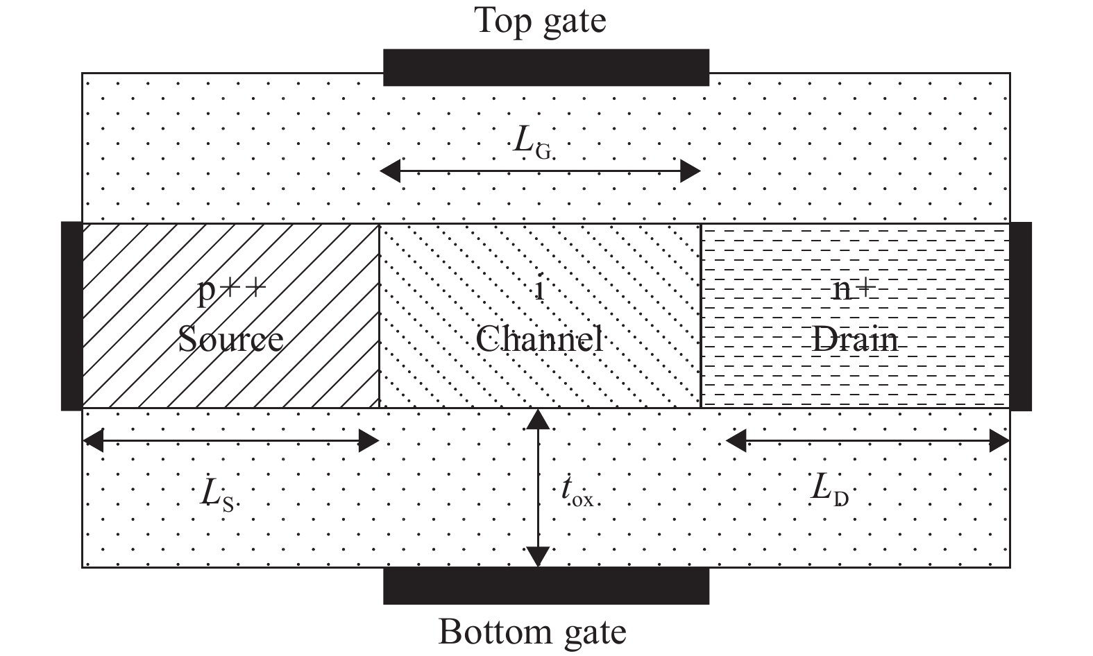
Fig. 1.
Schematic diagram for DG tunnel FET with high-k dielectric.
SEMICONDUCTOR DEVICES
Corresponding author: Shashi Bala, Email: shashi.sbbs@gmail.com
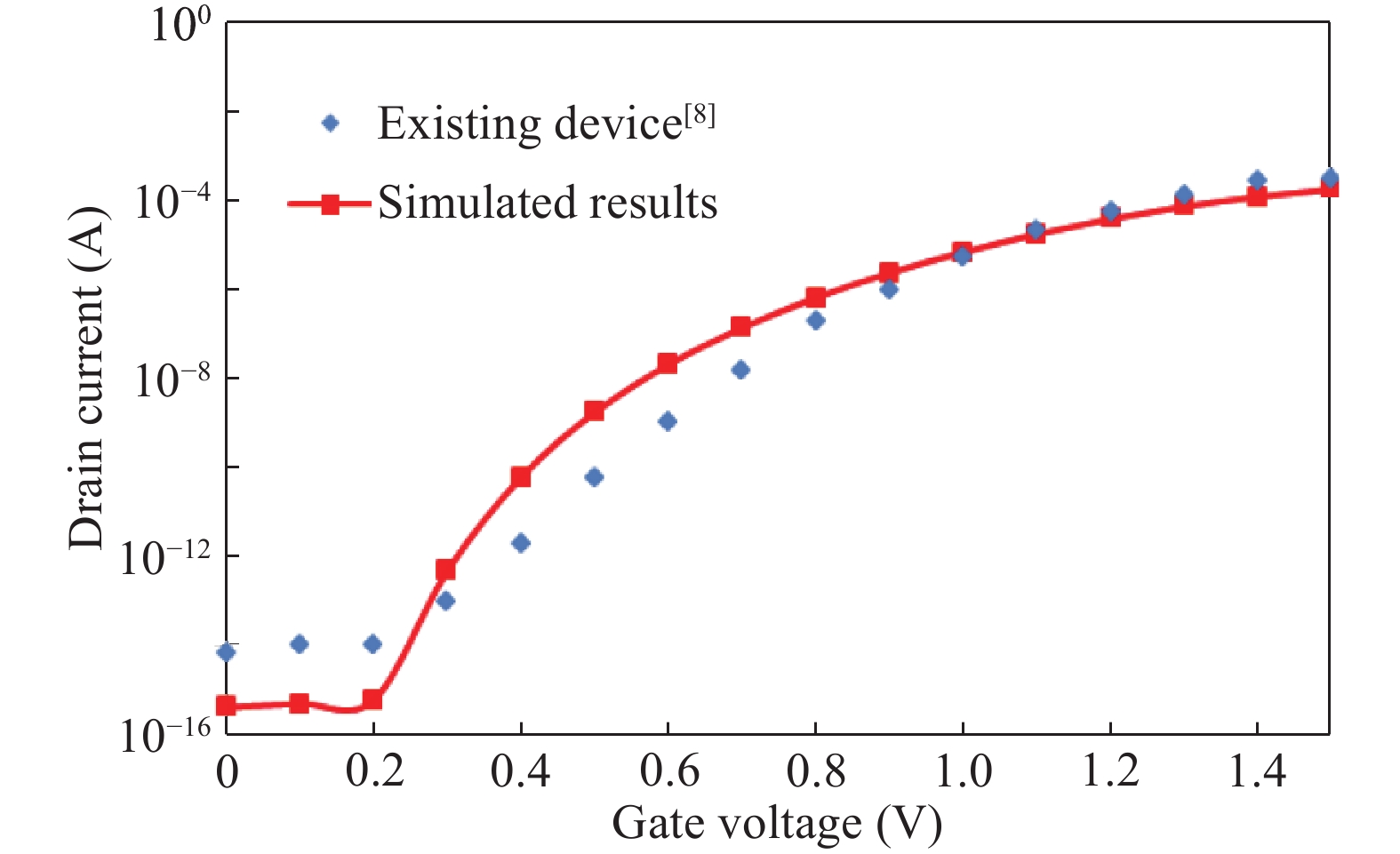
Abstract: A double-gate tunnel field-effect transistor (DG tunnel FET) has been designed and investigated for various channel materials such as silicon (Si), gallium arsenide (GaAs), alminium gallium arsenide (AlxGa1−xAs) and CNT using a nano ViDES Device and TCAD SILVACO ATLAS simulator. The proposed devices are compared on the basis of inverse subthreshold slope (SS), ION/IOFF current ratio and leakage current. Using Si as the channel material limits the property to reduce leakage current with scaling of channel, whereas the AlxGa1−xAs based DG tunnel FET provides a better ION/IOFF current ratio (2.51 × 10⁶) as compared to other devices keeping the leakage current within permissible limits. The performed silmulation of the CNT based channel in the double-gate tunnel field-effect transistor using the nano ViDES shows better performace for a sub-threshold slope of 29.4 mV/dec as the channel is scaled down. The proposed work shows the potential of the CNT channel based DG tunnel FET as a futuristic device for better switching and high retention time, which makes it suitable for memory based circuits.
Keywords: band-to-band tunneling (BTBT), double gate (DG), silicon (Si), gallium arsenide (GaAs), aluminum gallium arsenide (AlxGa1−xAs), tunnel field effect transistor (FET), carbon nanotube (CNT)
| [1] |
Sakurai T. Perspectives of low-power VLSI's. IEICE trans Electron, 2004, 87(4): 429
|
| [2] |
Bernstein K, Cavin R K, Porod W, et al. Device and architecture outlook for beyond CMOS switches. Proc IEEE, 2010, 98(12): 2169 doi: 10.1109/JPROC.2010.2066530
|
| [3] |
Seabaugh A C, Zhang Q. Low-voltage tunnel transistors for beyond CMOS logic. Proc IEEE, 2010, 98(12): 2095 doi: 10.1109/JPROC.2010.2070470
|
| [4] |
Zener C. A theory of the electrical breakdown of solid dielectrics. Proc Royal Soc London A, 1934, 145(855): 523 doi: 10.1098/rspa.1934.0116
|
| [5] |
Silvaco ATLAS device simulator and user manual, silvaco int; Santa Clara, CA, USA 5.19.2 2013
|
| [6] |
Appenzeller J, Lin Y M, Knoch J, et al. Comparing carbon nanotube transistors-the ideal choice: a novel tunneling device design. IEEE Trans Electron Devices, 2005, 52(12): 2568 doi: 10.1109/TED.2005.859654
|
| [7] |
Sharma S K, Raj B, Khosla M. Comparative analysis of MOSFET, CNTFET and NWFET for energy efficient VLSI circuit design. J VLSI Des Tools Technol, 2016, 6: 1
|
| [8] |
Boucart K, Ionescu A M. Length scaling of the double gate tunnel FET with a high-k gate dielectric. Solid-State Electron, 2007, 51(11): 1500
|
| [9] |
Sharma S K, Raj B, Khosla M. A Gaussian approach for analytical subthreshold current model of cylindrical nanowire FET with quantum mechanical effects. Microelectron J, 2016, 53: 65 doi: 10.1016/j.mejo.2016.04.002
|
| [10] |
Sharma S K, Raj B, Khosla M. Subthreshold performance of In1−xGaxAs based dual metal with gate stack cylindrical/surrounding gate nanowire MOSFET for low power analog applications. J Nanoelectron Optoelectron, 2017, 12(2): 171 doi: 10.1166/jno.2017.1961
|
| [11] |
Zhang L, Lin X, He J, et al. An analytical charge model for double-gate tunnel FETs. IEEE Trans Electron Devices, 2012, 59(12): 3217 doi: 10.1109/TED.2012.2217145
|
| [12] |
Kumar S, Raj B. Compact channel potential analytical modeling of DG-TFET based on Evanescent-mode approach. J Comput Electron, 2015, 14(3): 820 doi: 10.1007/s10825-015-0718-9
|
| [13] |
Singh A, Khosla M, Raj B. Analysis of electrostatic doped Schottky barrier carbon nanotube FET for low power applications. J Mater Sci: Mater Electron, 2017, 28(2): 1762 doi: 10.1007/s10854-016-5723-7
|
| [14] |
Singh K, Raj B. Temperature-dependent modeling and performance evaluation of multi-walled CNT and single-walled CNT as global interconnects. J Electron Mater, 2015, 44(12): 4825 doi: 10.1007/s11664-015-4040-x
|
| [15] |
Narang R, Saxena M, Gupta M, et al. Modeling and simulation of multi layer gate dielectric double gate tunnel field-effect transistor (DG-TFET). Students' Technology Symposium (TechSym), 2011: 281
|
| [16] |
Kumar S, Raj B. Analysis of ION and ambipolar current for dual-material gate–drain overlapped DG-TFET. J Nanoelectron Optoelectron, 2016, 11(3): 323 doi: 10.1166/jno.2016.1902
|
| [17] |
Singh K, Raj B. Performance and analysis of temperature dependent multi-walled carbon nanotubes as global interconnects at different technology nodes. J Comput Electron, 2015, 14(2): 469 doi: 10.1007/s10825-015-0667-3
|
| [18] |
Krishnamohan T, Kim D, Raghunathan S, et al. Double-gate strained-Ge heterostructure tunneling FET (TFET) with record high drive currents and
|
| [19] |
Arun S, Balamurugan N B. An analytical modeling and simulation of dual material double gate tunnel field effect transistor for low power applications. J Electr Eng Technol, 2014, 9(1): 247 doi: 10.5370/JEET.2014.9.1.247
|
| [20] |
Singh A, Khosla M, Raj B. Compact model for ballistic single wall CNTFET under quantum capacitance limit. J Semicond, 2016, 37(10): 104001 doi: 10.1088/1674-4926/37/10/104001
|
| [21] |
Sahoo R, Mishra R R. Simulations of carbon nanotube field effect transistors. Int J Electron Eng Res, 2009, 1(2): 117
|
| [22] |
Singh A, Khosla M, Raj B. Compact model for ballistic single wall CNTFET under quantum capacitance limit. J Semicond, 2016, 37(10): 104001 doi: 10.1088/1674-4926/37/10/104001
|
| [23] |
Singh A, Khosla M, Raj B. Comparative analysis of carbon nanotube field effect transistor and nanowire transistor for low power circuit design. J Nanoelectron Optoelectron, 2016, 11(3): 388 doi: 10.1166/jno.2016.1913
|
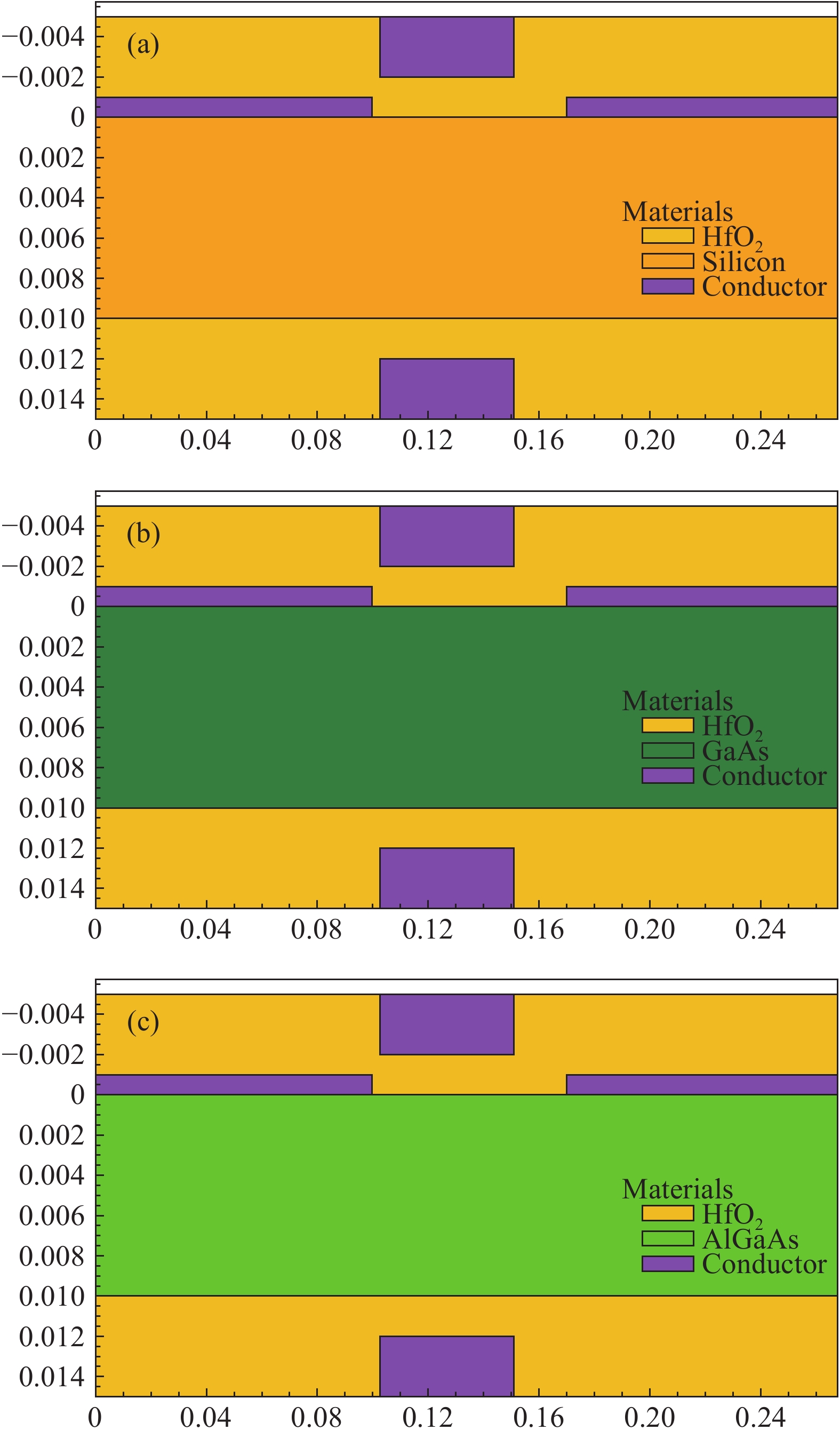
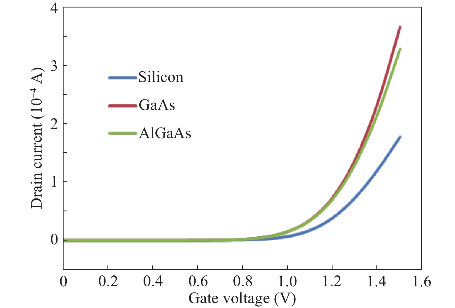
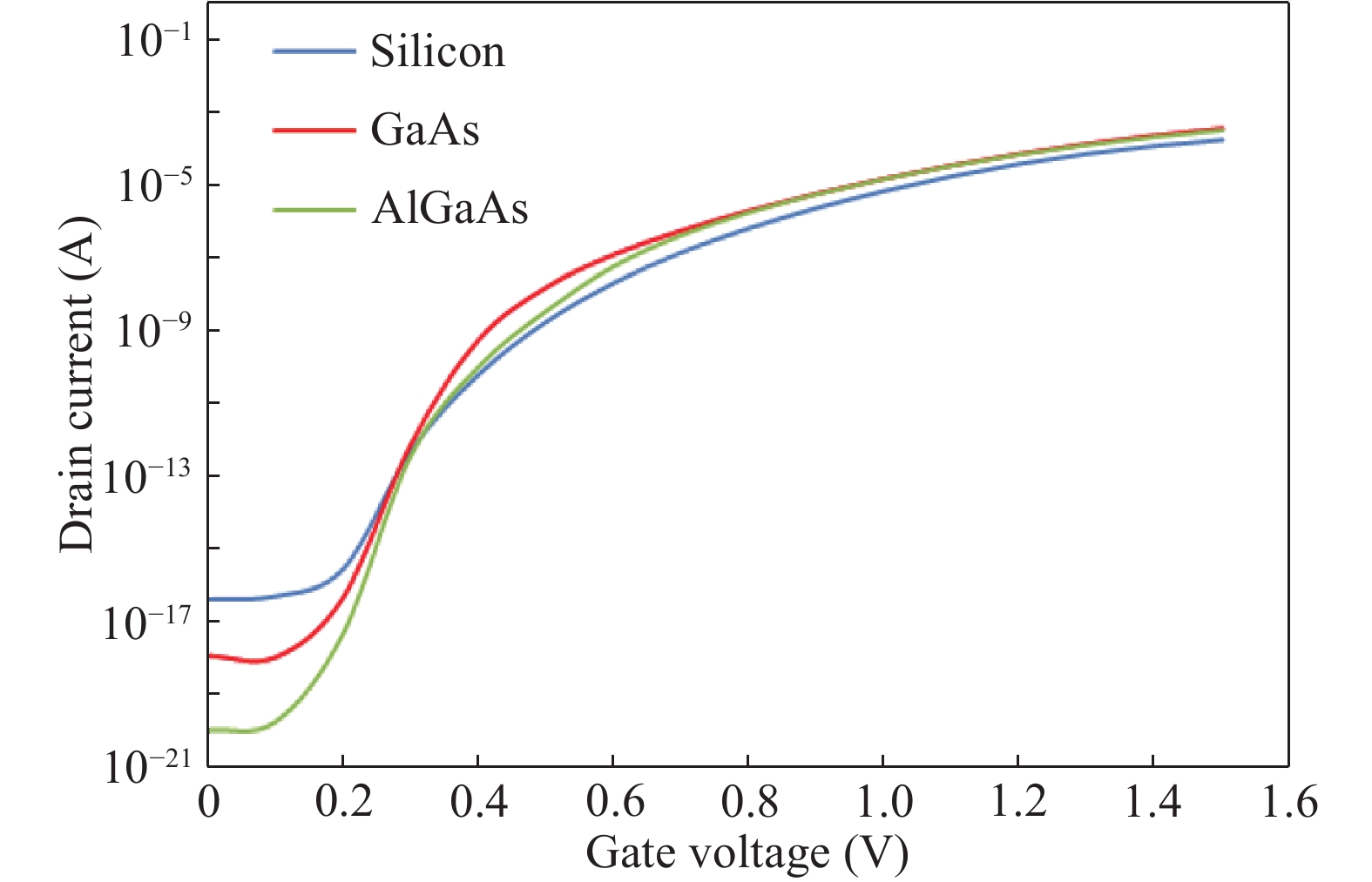
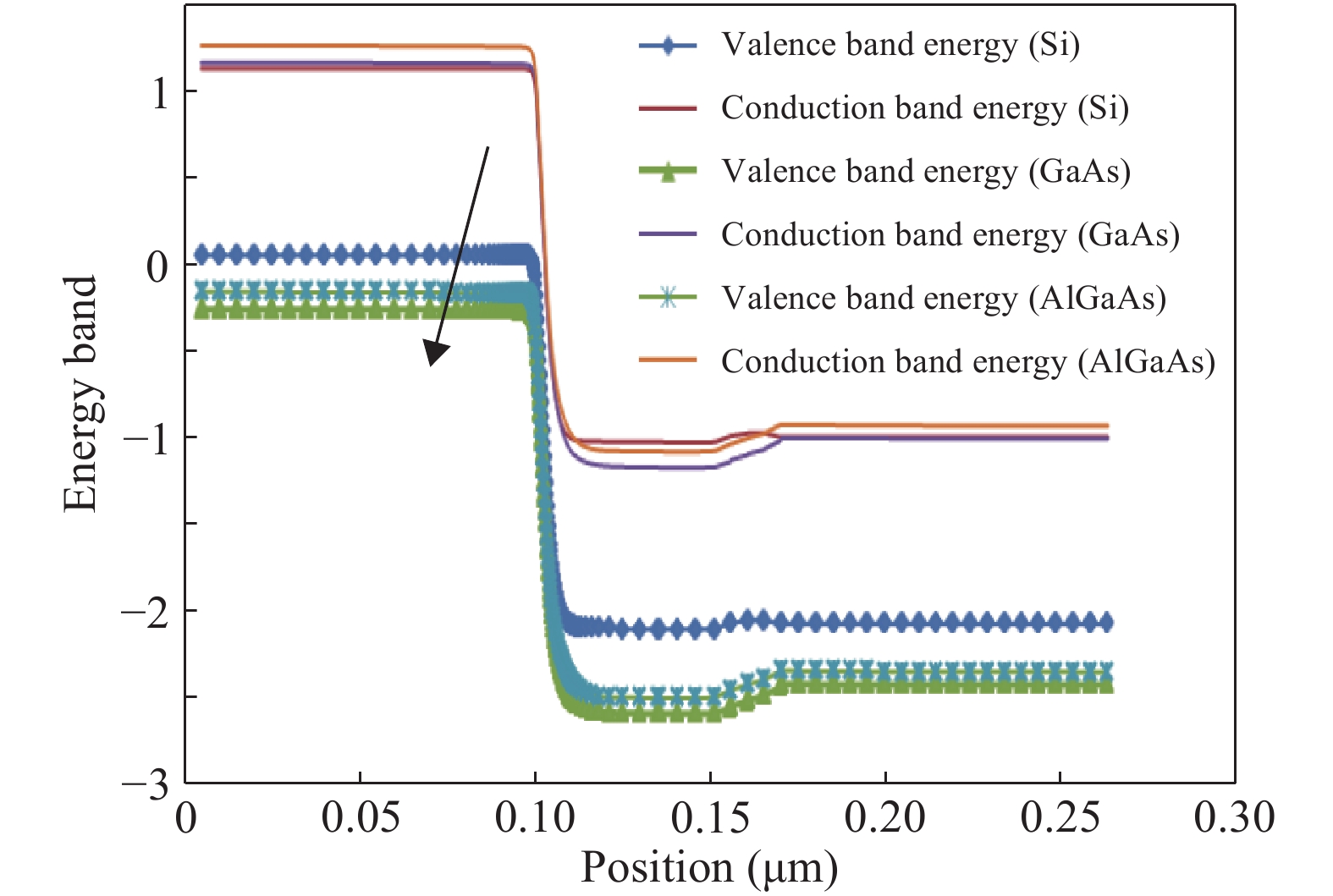
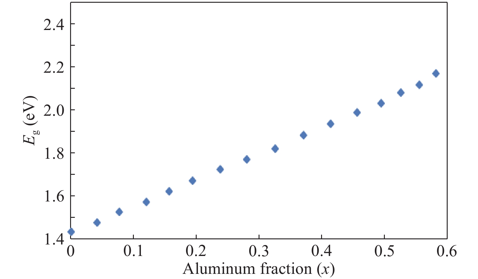
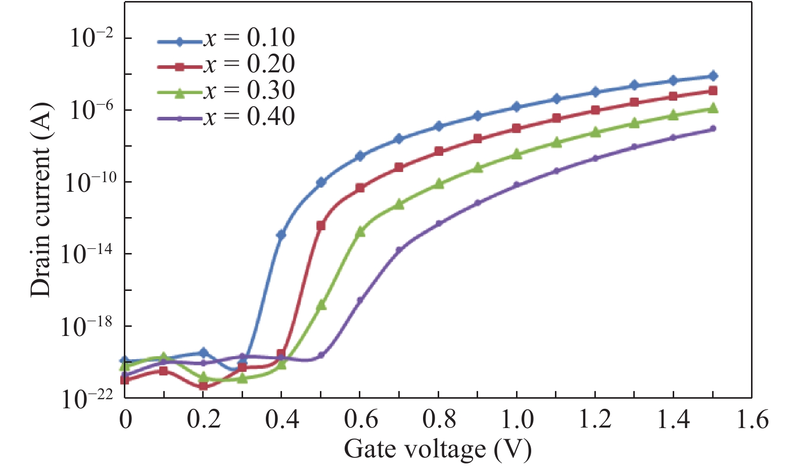
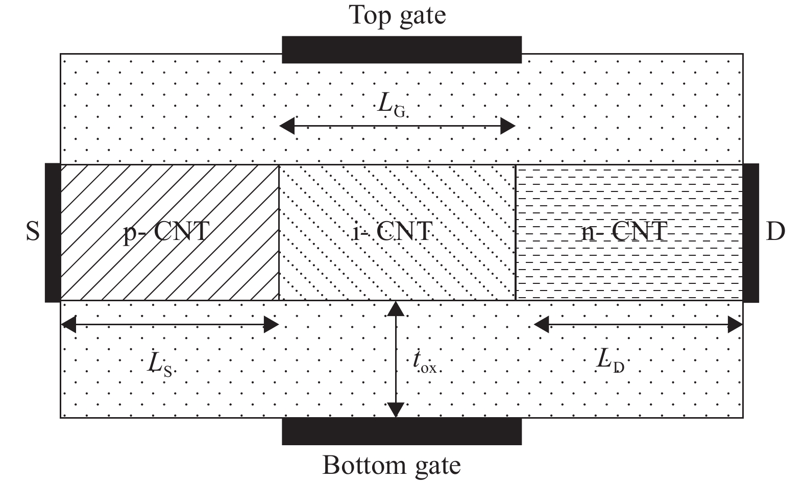
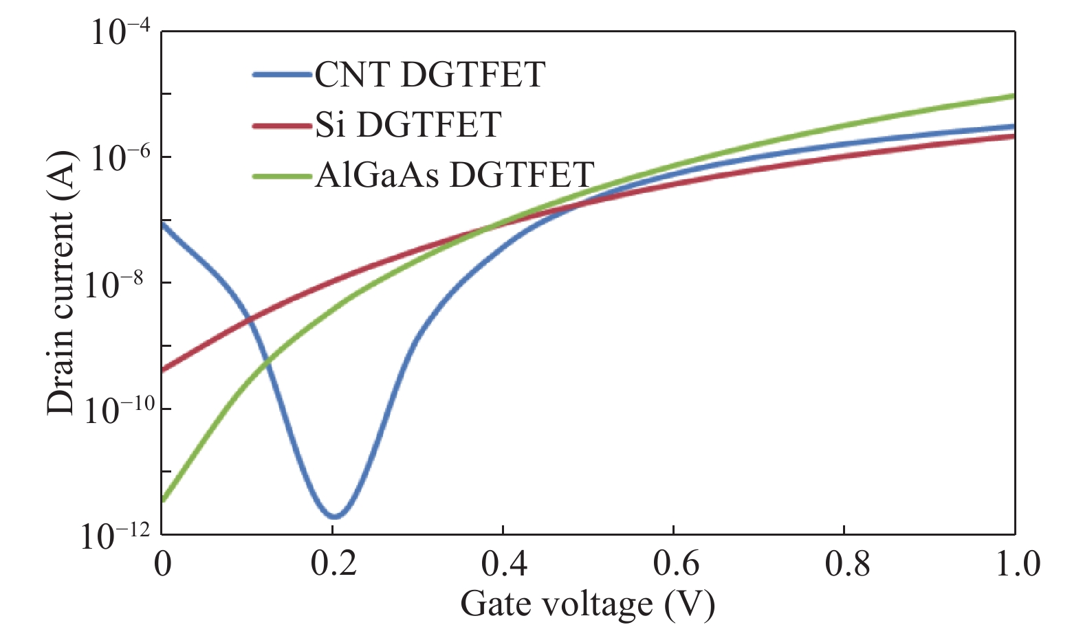
Table 1. Properties of the various channel materials used in SILVACO ATLAS TCAD simulation.
| Property | Si | GaAs | AlxGa1−xAs | CNT |
| Dielectric constant | 11.9 | 13.1 | 12.90−2.84x | 4.8 |
| Energy gap at 300 K (eV) | 1.12 | 1.424 | 1.422 eV + 1.2475x | 0.75 |
| Intrinsic carrier concentration (cm−3) | 1.45 × 10¹⁰ | 1.79 × 10⁶ | 2.1 × 10⁵ | – |
| Mobility (Drift) μn (cm2/(V·s)) | 1500 | 8500 | 8.1−2.2x + 104x2 | 79 000 |
| Mobility (Drift) μp (cm2/(V·s)) | 475 | 400 | 370−970x + 740x2 | 79 000 |
| Thermal conductivity at 300 K (W/cm·°C) | 1.5 | 0.46 | 0.55−2.12x + 2.48x2 | 6600 |
 DownLoad: CSV
Table 2. Various output parameters for different channel materials (SILVACO ATLAS TCAD simulation).
| Device with different channel materials | IOFF | ION | ION/IOFF | SS (mV/decade) | Vt |
| Silicon | 4.11 × 10⁻¹⁷ | 17.7 × 10⁻⁵ | 4.32 × 10¹² | 30.7985 | 0.682591 |
| GaAs | 1.16 × 10⁻¹⁸ | 36.6 × 10⁻⁵ | 3.15 × 10¹⁴ | 16.121 | 0.590537 |
| AlGaAs | 1.01 × 10⁻²⁰ | 32.8 × 10⁻⁵ | 3.24 × 10¹⁶ | 14.5095 | 0.627576 |
DownLoad: CSV
Table 3. Various output parameters for different mole fractions of aluminum.
| Mole fraction | IOFF | ION | ION/IOFF | SS (mV/decade) | Vt |
| x = 10 | 1.24 × 10⁻²¹ | 7.70 × 10⁻⁵ | 6.21 × 10¹⁶ | 14.074 | 0.785767 |
| x = 20 | 1.18 × 10⁻²¹ | 1.19 × 10⁻⁵ | 1.01 × 10¹⁶ | 14.1381 | 1.00271 |
| x = 30 | 6.86 × 10⁻²¹ | 1.24 × 10⁻⁶ | 1.81 × 10¹⁴ | 24.6429 | 1.24419 |
| x = 40 | 2.20 × 10⁻²¹ | 8.67 × 10⁻⁸ | 3.94 × 10¹³ | 27.9075 | 1.3300 |
DownLoad: CSV
Table 4. Various output parameters for different channel materials obtained from TCAD simulation.
| Device with different channel materials | ION | IOFF | ION/IOFF | SS (mV/decade) |
| Silicon | 2.14 × 10⁻⁶ | 4.27 × 10⁻¹⁰ | 5.011 × 10³ | 37 |
| AlxGa1−xAs | 9.30 × 10⁻⁶ | 3.70 × 10⁻¹² | 2.51 × 10⁶ | 32.5 |
| CNT (d = 1 nm) | 3.03 × 10⁻⁶ | 2.00 × 10⁻¹² | 1.51 × 10⁶ | 29.4 |
DownLoad: CSV
| [1] |
Sakurai T. Perspectives of low-power VLSI's. IEICE trans Electron, 2004, 87(4): 429
|
| [2] |
Bernstein K, Cavin R K, Porod W, et al. Device and architecture outlook for beyond CMOS switches. Proc IEEE, 2010, 98(12): 2169 doi: 10.1109/JPROC.2010.2066530
|
| [3] |
Seabaugh A C, Zhang Q. Low-voltage tunnel transistors for beyond CMOS logic. Proc IEEE, 2010, 98(12): 2095 doi: 10.1109/JPROC.2010.2070470
|
| [4] |
Zener C. A theory of the electrical breakdown of solid dielectrics. Proc Royal Soc London A, 1934, 145(855): 523 doi: 10.1098/rspa.1934.0116
|
| [5] |
Silvaco ATLAS device simulator and user manual, silvaco int; Santa Clara, CA, USA 5.19.2 2013
|
| [6] |
Appenzeller J, Lin Y M, Knoch J, et al. Comparing carbon nanotube transistors-the ideal choice: a novel tunneling device design. IEEE Trans Electron Devices, 2005, 52(12): 2568 doi: 10.1109/TED.2005.859654
|
| [7] |
Sharma S K, Raj B, Khosla M. Comparative analysis of MOSFET, CNTFET and NWFET for energy efficient VLSI circuit design. J VLSI Des Tools Technol, 2016, 6: 1
|
| [8] |
Boucart K, Ionescu A M. Length scaling of the double gate tunnel FET with a high-k gate dielectric. Solid-State Electron, 2007, 51(11): 1500
|
| [9] |
Sharma S K, Raj B, Khosla M. A Gaussian approach for analytical subthreshold current model of cylindrical nanowire FET with quantum mechanical effects. Microelectron J, 2016, 53: 65 doi: 10.1016/j.mejo.2016.04.002
|
| [10] |
Sharma S K, Raj B, Khosla M. Subthreshold performance of In1−xGaxAs based dual metal with gate stack cylindrical/surrounding gate nanowire MOSFET for low power analog applications. J Nanoelectron Optoelectron, 2017, 12(2): 171 doi: 10.1166/jno.2017.1961
|
| [11] |
Zhang L, Lin X, He J, et al. An analytical charge model for double-gate tunnel FETs. IEEE Trans Electron Devices, 2012, 59(12): 3217 doi: 10.1109/TED.2012.2217145
|
| [12] |
Kumar S, Raj B. Compact channel potential analytical modeling of DG-TFET based on Evanescent-mode approach. J Comput Electron, 2015, 14(3): 820 doi: 10.1007/s10825-015-0718-9
|
| [13] |
Singh A, Khosla M, Raj B. Analysis of electrostatic doped Schottky barrier carbon nanotube FET for low power applications. J Mater Sci: Mater Electron, 2017, 28(2): 1762 doi: 10.1007/s10854-016-5723-7
|
| [14] |
Singh K, Raj B. Temperature-dependent modeling and performance evaluation of multi-walled CNT and single-walled CNT as global interconnects. J Electron Mater, 2015, 44(12): 4825 doi: 10.1007/s11664-015-4040-x
|
| [15] |
Narang R, Saxena M, Gupta M, et al. Modeling and simulation of multi layer gate dielectric double gate tunnel field-effect transistor (DG-TFET). Students' Technology Symposium (TechSym), 2011: 281
|
| [16] |
Kumar S, Raj B. Analysis of ION and ambipolar current for dual-material gate–drain overlapped DG-TFET. J Nanoelectron Optoelectron, 2016, 11(3): 323 doi: 10.1166/jno.2016.1902
|
| [17] |
Singh K, Raj B. Performance and analysis of temperature dependent multi-walled carbon nanotubes as global interconnects at different technology nodes. J Comput Electron, 2015, 14(2): 469 doi: 10.1007/s10825-015-0667-3
|
| [18] |
Krishnamohan T, Kim D, Raghunathan S, et al. Double-gate strained-Ge heterostructure tunneling FET (TFET) with record high drive currents and
|
| [19] |
Arun S, Balamurugan N B. An analytical modeling and simulation of dual material double gate tunnel field effect transistor for low power applications. J Electr Eng Technol, 2014, 9(1): 247 doi: 10.5370/JEET.2014.9.1.247
|
| [20] |
Singh A, Khosla M, Raj B. Compact model for ballistic single wall CNTFET under quantum capacitance limit. J Semicond, 2016, 37(10): 104001 doi: 10.1088/1674-4926/37/10/104001
|
| [21] |
Sahoo R, Mishra R R. Simulations of carbon nanotube field effect transistors. Int J Electron Eng Res, 2009, 1(2): 117
|
| [22] |
Singh A, Khosla M, Raj B. Compact model for ballistic single wall CNTFET under quantum capacitance limit. J Semicond, 2016, 37(10): 104001 doi: 10.1088/1674-4926/37/10/104001
|
| [23] |
Singh A, Khosla M, Raj B. Comparative analysis of carbon nanotube field effect transistor and nanowire transistor for low power circuit design. J Nanoelectron Optoelectron, 2016, 11(3): 388 doi: 10.1166/jno.2016.1913
|


Article views: 7882 Times PDF downloads: 405 Times Cited by: 0 Times
Received: 21 July 2017 Revised: 09 August 2017 Online: Uncorrected proof: 25 January 2018Accepted Manuscript: 02 March 2018Published: 01 April 2018
| Citation: |
Shashi Bala, Mamta Khosla. Design and simulation of nanoscale double-gate TFET/tunnel CNTFET[J]. Journal of Semiconductors, 2018, 39(4): 044001. doi: 10.1088/1674-4926/39/4/044001
****
S S B la, M Khosla. Design and simulation of nanoscale double-gate TFET/tunnel CNTFET[J]. J. Semicond., 2018, 39(4): 044001. doi: 10.1088/1674-4926/39/4/044001.

|
| [1] |
Sakurai T. Perspectives of low-power VLSI's. IEICE trans Electron, 2004, 87(4): 429
|
| [2] |
Bernstein K, Cavin R K, Porod W, et al. Device and architecture outlook for beyond CMOS switches. Proc IEEE, 2010, 98(12): 2169 doi: 10.1109/JPROC.2010.2066530
|
| [3] |
Seabaugh A C, Zhang Q. Low-voltage tunnel transistors for beyond CMOS logic. Proc IEEE, 2010, 98(12): 2095 doi: 10.1109/JPROC.2010.2070470
|
| [4] |
Zener C. A theory of the electrical breakdown of solid dielectrics. Proc Royal Soc London A, 1934, 145(855): 523 doi: 10.1098/rspa.1934.0116
|
| [5] |
Silvaco ATLAS device simulator and user manual, silvaco int; Santa Clara, CA, USA 5.19.2 2013
|
| [6] |
Appenzeller J, Lin Y M, Knoch J, et al. Comparing carbon nanotube transistors-the ideal choice: a novel tunneling device design. IEEE Trans Electron Devices, 2005, 52(12): 2568 doi: 10.1109/TED.2005.859654
|
| [7] |
Sharma S K, Raj B, Khosla M. Comparative analysis of MOSFET, CNTFET and NWFET for energy efficient VLSI circuit design. J VLSI Des Tools Technol, 2016, 6: 1
|
| [8] |
Boucart K, Ionescu A M. Length scaling of the double gate tunnel FET with a high-k gate dielectric. Solid-State Electron, 2007, 51(11): 1500
|
| [9] |
Sharma S K, Raj B, Khosla M. A Gaussian approach for analytical subthreshold current model of cylindrical nanowire FET with quantum mechanical effects. Microelectron J, 2016, 53: 65 doi: 10.1016/j.mejo.2016.04.002
|
| [10] |
Sharma S K, Raj B, Khosla M. Subthreshold performance of In1−xGaxAs based dual metal with gate stack cylindrical/surrounding gate nanowire MOSFET for low power analog applications. J Nanoelectron Optoelectron, 2017, 12(2): 171 doi: 10.1166/jno.2017.1961
|
| [11] |
Zhang L, Lin X, He J, et al. An analytical charge model for double-gate tunnel FETs. IEEE Trans Electron Devices, 2012, 59(12): 3217 doi: 10.1109/TED.2012.2217145
|
| [12] |
Kumar S, Raj B. Compact channel potential analytical modeling of DG-TFET based on Evanescent-mode approach. J Comput Electron, 2015, 14(3): 820 doi: 10.1007/s10825-015-0718-9
|
| [13] |
Singh A, Khosla M, Raj B. Analysis of electrostatic doped Schottky barrier carbon nanotube FET for low power applications. J Mater Sci: Mater Electron, 2017, 28(2): 1762 doi: 10.1007/s10854-016-5723-7
|
| [14] |
Singh K, Raj B. Temperature-dependent modeling and performance evaluation of multi-walled CNT and single-walled CNT as global interconnects. J Electron Mater, 2015, 44(12): 4825 doi: 10.1007/s11664-015-4040-x
|
| [15] |
Narang R, Saxena M, Gupta M, et al. Modeling and simulation of multi layer gate dielectric double gate tunnel field-effect transistor (DG-TFET). Students' Technology Symposium (TechSym), 2011: 281
|
| [16] |
Kumar S, Raj B. Analysis of ION and ambipolar current for dual-material gate–drain overlapped DG-TFET. J Nanoelectron Optoelectron, 2016, 11(3): 323 doi: 10.1166/jno.2016.1902
|
| [17] |
Singh K, Raj B. Performance and analysis of temperature dependent multi-walled carbon nanotubes as global interconnects at different technology nodes. J Comput Electron, 2015, 14(2): 469 doi: 10.1007/s10825-015-0667-3
|
| [18] |
Krishnamohan T, Kim D, Raghunathan S, et al. Double-gate strained-Ge heterostructure tunneling FET (TFET) with record high drive currents and
|
| [19] |
Arun S, Balamurugan N B. An analytical modeling and simulation of dual material double gate tunnel field effect transistor for low power applications. J Electr Eng Technol, 2014, 9(1): 247 doi: 10.5370/JEET.2014.9.1.247
|
| [20] |
Singh A, Khosla M, Raj B. Compact model for ballistic single wall CNTFET under quantum capacitance limit. J Semicond, 2016, 37(10): 104001 doi: 10.1088/1674-4926/37/10/104001
|
| [21] |
Sahoo R, Mishra R R. Simulations of carbon nanotube field effect transistors. Int J Electron Eng Res, 2009, 1(2): 117
|
| [22] |
Singh A, Khosla M, Raj B. Compact model for ballistic single wall CNTFET under quantum capacitance limit. J Semicond, 2016, 37(10): 104001 doi: 10.1088/1674-4926/37/10/104001
|
| [23] |
Singh A, Khosla M, Raj B. Comparative analysis of carbon nanotube field effect transistor and nanowire transistor for low power circuit design. J Nanoelectron Optoelectron, 2016, 11(3): 388 doi: 10.1166/jno.2016.1913
|

 WeChat ID
Journal of Semiconductors © 2017 All Rights Reserved 京ICP备05085259号-2