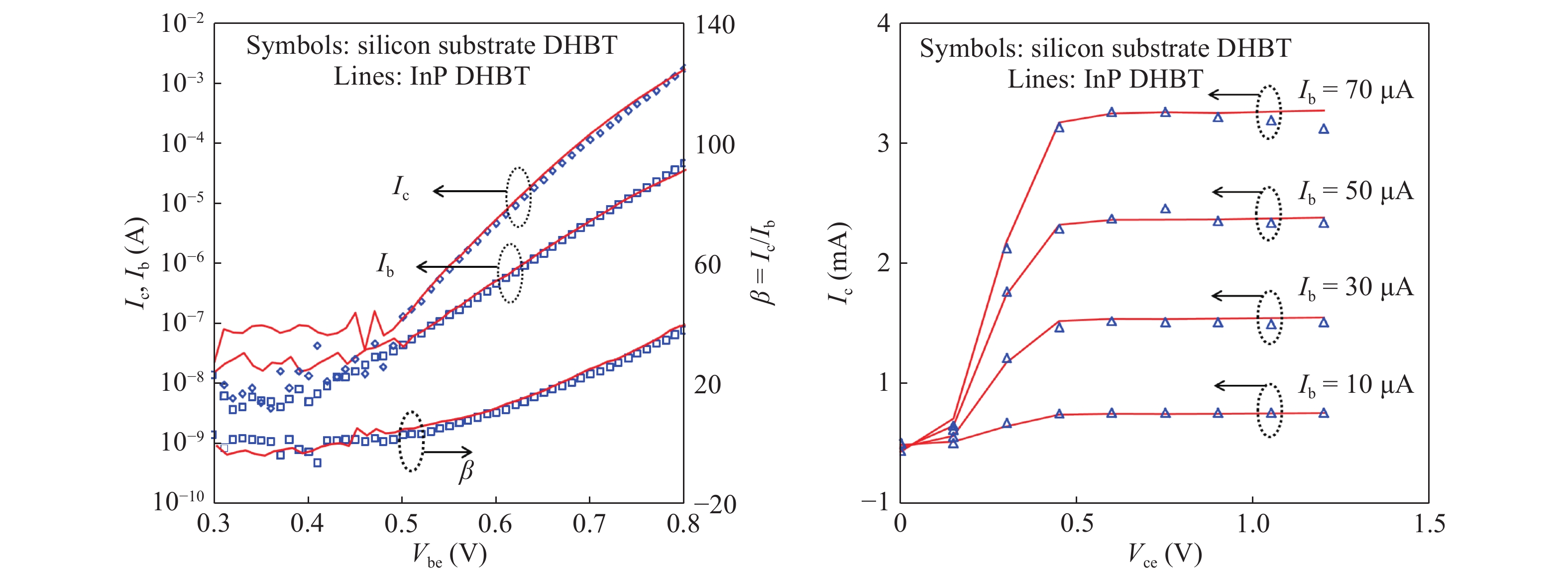
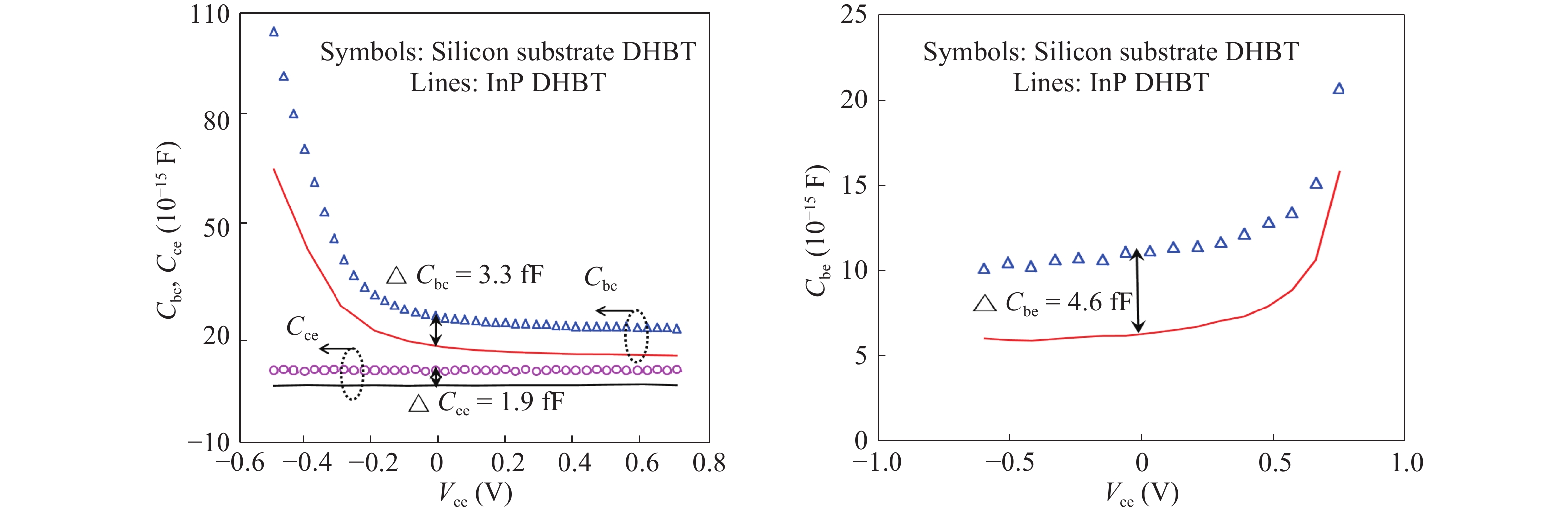
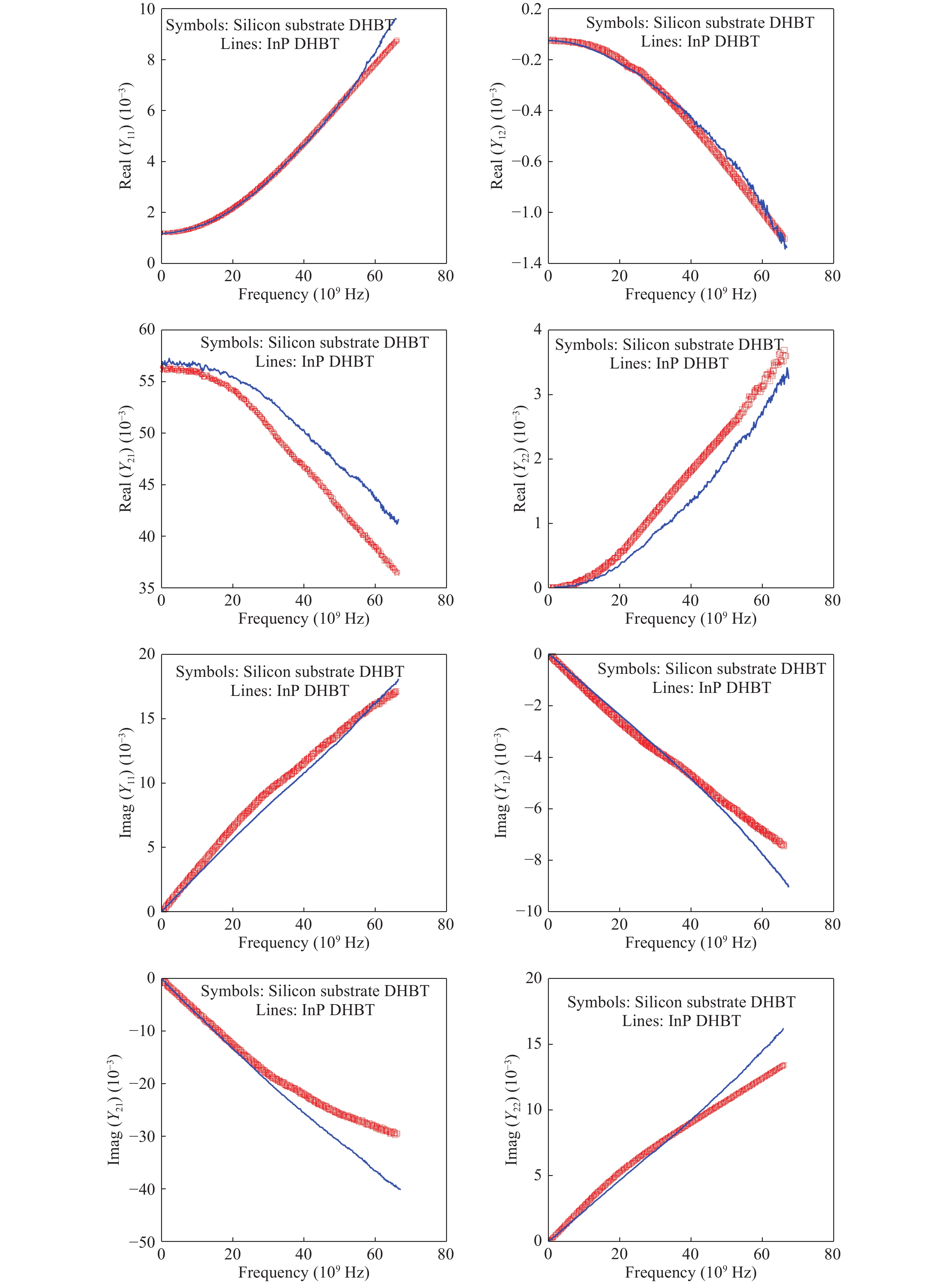
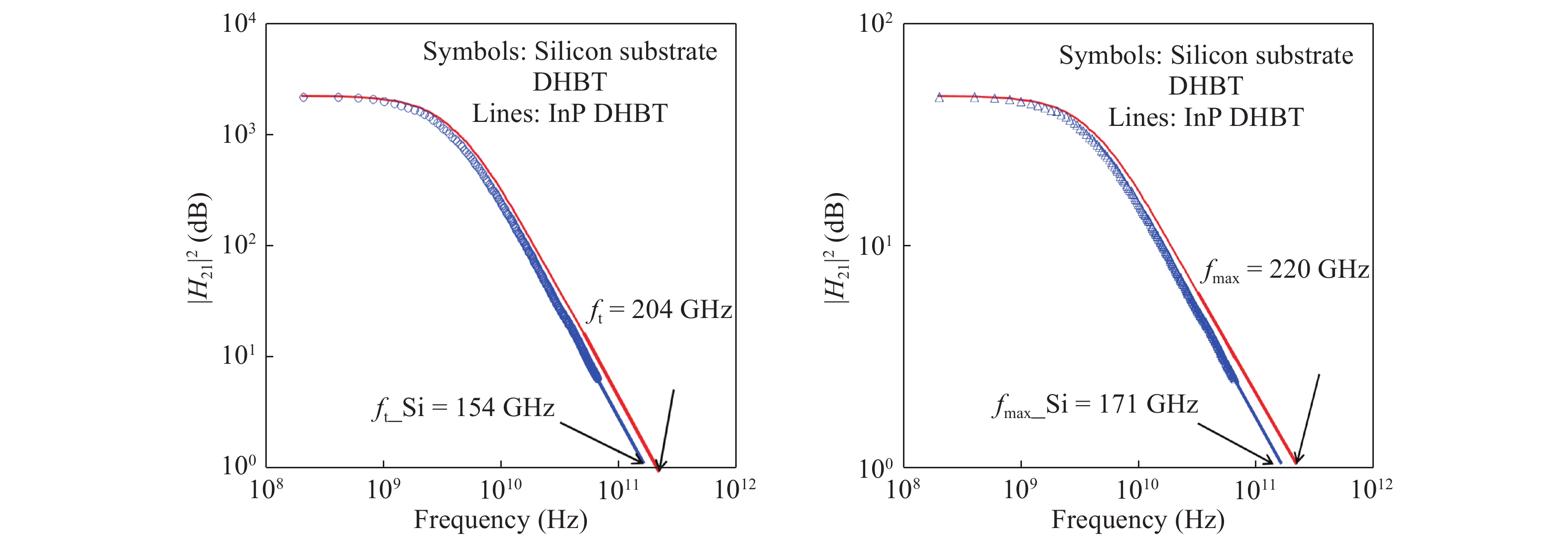
| [1] |
Yamada H, Onozuka Y, Iida A, et al. A wafer-level heterogeneous technology integration for flexible pseudo-SoC. IEEE International Solid-State Circuits Conference, 2010: 146 doi: 10.1109/ISSCC.2010.5434011 |
| [2] |
Matsuzawa A. A new direction in integrated circuit technology. 50th Midwest Symposium on Circuits & Systems, 2007: 1550 doi: 10.1109/MWSCAS.2007.4488837 |
| [3] |
Ancey P. From 3D-SOC to 3D heterogeneous systems: technology and applications. Symposium on VLSI Technology, Honolulu, HI, USA, 2011: 180
|
| [4] |
Ostermay I. 200 GHz interconnects for InP-on-BiCMOS integration. IEEE MTT-S International Microwave Symposium, Seattle, WA, USA, 2013: 1 doi: 10.1109/MWSYM.2013.6697393 |
| [5] |
Royter Y, Patterson P R, Li J C, et al. Dense heterogeneous integration for InP Bi-CMOS technology. IEEE International Conference on Indium Phosphide & Related Materials, 2009: 105 doi: 10.1109/ICIPRM.2009.5012453 |
| [6] |
Kazior T E, LaRoche J R, Lubyshev D, et al. A high performance differential amplifier through the direct monolithic integration of InP HBTs and Si CMOS on silicon substrates. IEEE MTT-S International Microwave Symposium Digest, 2009: 1113 doi: 10.1109/MWSYM.2009.5165896 |
| [7] |
Hossain M, Nosaeva K, Weimann N, et al. A 330 GHz active frequency quadrupler in InP DHBT transferred-substrate technology. IEEE MTT-S International Microwave Symposium, 2016: 1 doi: 10.1109/MWSYM.2016.7540049 |
| [8] |
Liou J C, Yang C F, Lin Y C, et al. Monolithic of SOI wafer waveguide and InP-laser with DVS-BCB coating and bonding. Microelectron Eng, 2015, 148: 44 doi: 10.1016/j.mee.2015.07.010 |
| [9] |
Wang J, Yang X, Niu Y, et al. ICP-RIE dry etching of 4H-SiC materials in SF6/O2/HBr. Micronanoelectron Technol, 2015, 52: 59
|
| [10] |
Tiemeijer L F, Havens R J, Jansman A B M, et al. Comparison of the "pad-open-short" and "open-short-load" deembedding techniques for accurate on-wafer RF characterization of high-quality passives. IEEE Trans Microwave Theory Tech, 2005, 53(2): 723 doi: 10.1109/TMTT.2004.840621 |
| [11] |
Potereau M, Raya C, Matos M D, et al. Limitations of on-wafer calibration and de-embedding methods in the sub-THz range. J Comput Commun, 2013, 01(6): 25 doi: 10.4236/jcc.2013.16005 |
| [12] |
Johansen T K, Leblanc R, Poulain J, et al. Direct extraction of InP/GaAsSb/InP DHBT equivalent-circuit elements from S-parameters measured at cut-off and normal bias conditions. IEEE Trans Microwave Theory Tech, 2016, 64(1): 115 doi: 10.1109/TMTT.2015.2503769 |
| [13] |
Lee K, Choi K, Kook S H, et al. Direct parameter extraction of SiGe HBTs for the VBIC bipolar compact model. IEEE Trans Electron Devices, 2005, 52(3): 375 doi: 10.1109/TED.2005.843906 |
| [14] |
Zhou Z J, Ren K, Liu J, et al. Frequency stability of InP HBT over 0.2 to 220 GHz. J Semicond, 2015, 36(2): 024006 doi: 10.1088/1674-4926/36/2/024006 |
| [15] |
Lee S. A parameter extraction method for a small-signal MOSFET model including substrate parameters. IEEE International Conference on Semiconductor Electronics, 2002: 255 doi: 10.1109/SMELEC.2002.1217819 |


 DownLoad: