


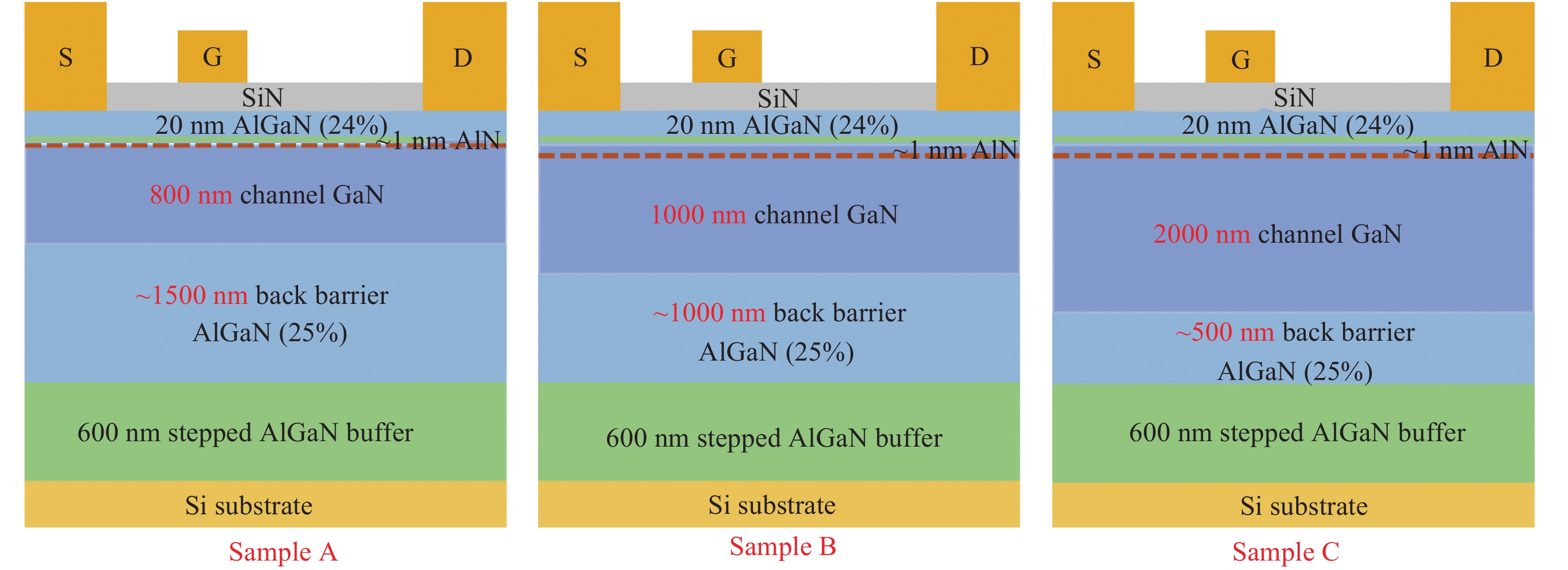
Fig. 1.
(Color online) Schematic diagrams of AlGaN/GaN HEMT structures for three samples.
SEMICONDUCTOR DEVICES
Jie Zhao1, 2, Yanhui Xing1, Kai Fu2, Peipei Zhang3, Liang Song2, Fu Chen2, Taotao Yang1, 2, Xuguang Deng2, Sen Zhang4 and Baoshun Zhang2, 5,
Corresponding author: Baoshun Zhang, bszhang2006@sinano.ac.cn
Abstract: The leakage current and breakdown voltage of AlGaN/GaN/AlGaN high electron mobility transistors on silicon with different GaN channel thicknesses were investigated. The results showed that a thin GaN channel was beneficial for obtaining a high breakdown voltage, based on the leakage current path and the acceptor traps in the AlGaN back-barrier. The breakdown voltage of the device with an 800 nm-thick GaN channel was 926 V @ 1 mA/mm, and the leakage current increased slowly between 300 and 800 V. Besides, the raising conduction band edge of the GaN channel by the AlGaN back-barrier lead to little degradation for sheet 2-D electron gas density, especially, in the thin GaN channel. The transfer and output characteristics were not obviously deteriorated for the samples with different GaN channel thickness. Through optimizing the GaN channel thickness and designing the AlGaN back-barrier, the lower leakage current and higher breakdown voltage would be possible.
Keywords: AlGaN/GaN high electronic mobility transistors, AlGaN back-barrier, breakdown characteristics, leakage current path, Si substrate
| [1] |
Ueda T, Ishida M, Tanaka T, et al. GaN transistors on Si for switching and high-frequency applications. Jpn J Appl Phys, 2014, 53(10): 100214 doi: 10.7567/JJAP.53.100214
|
| [2] |
Xin T, Yuan J, Gu G, et al. High performance AlGaN/GaN HEMTs with AlN/SiNx passivation. J Semicond, 2015, 36(7): 074008 doi: 10.1088/1674-4926/36/7/074008
|
| [3] |
Yatabe Z, Asubar J T, Hashizume T. Insulated gate and surface passivation structures for GaN-based power transistors. J Phys D, 2016, 49(39): 393001 doi: 10.1088/0022-3727/49/39/393001
|
| [4] |
Zhang Z, Qin S, Fu K, et al. Fabrication of normally-off AlGaN/GaN metal–insulator–semiconductor high-electron-mobility transistors by photo-electrochemical gate recess etching in ionic liquid. Appl Phys Express, 2016, 9(8): 084102 doi: 10.7567/APEX.9.084102
|
| [5] |
Katsuno T, Manaka T, Ishikawa T, et al. Current collapse imaging of Schottky gate AlGaN/GaN high electron mobility transistors by electric field-induced optical second-harmonic generation measurement. Appl Phys Lett, 2014, 104(25): 1742
|
| [6] |
Medjdoub F, Zegaoui M, Grimbert B, et al. Effects of AlGaN back barrier on AlN/GaN-on-silicon high-electron-mobility transistors. Appl Phys Express, 2011, 4(12): 4101
|
| [7] |
Bahat-Treidel E, Hilt O, Brunner F, et al. Punch-through voltage enhancement scaling of AlGaN/GaN HEMTs using AlGaN double heterojunction confinement. IEEE Trans Electron Devices, 2008, 55(12): 3354 doi: 10.1109/TED.2008.2006891
|
| [8] |
Kelekci O, Tasli P, Cetin S S, et al. Investigation of AlInN HEMT structures with different AlGaN buffer layers grown on sapphire substrates by MOCVD. Curr Appl Phys, 2012, 12(6): 1600 doi: 10.1016/j.cap.2012.05.040
|
| [9] |
Ravikiran L, Dharmarasu N, Radhakrishnan K, et al. Growth and characterization of AlGaN/GaN/AlGaN double-heterojunction high-electron-mobility transistors on 100-mm Si(111) using ammonia-molecular beam epitaxy. J Appl Phys, 2015, 117(2): 091003
|
| [10] |
Wang X, Huang S, Zheng Y, et al. Effect of GaN channel layer thickness on DC and RF performance of GaN HEMTs with composite AlGaN/GaN buffer. IEEE Trans Electron Devices, 2014, 61(5): 1341 doi: 10.1109/TED.2014.2312232
|
| [11] |
Zanandrea A, Bahat-Treidel E, Rampazzo F, et al. Single- and double-heterostructure GaN-HEMTs devices for power switching applications. Microelectron Reliab, 2012, 52(9/10): 2426
|
| [12] |
Hsiao Y L, Chang C A, Chang E, et al. Material growth and device characterization of AlGaN/GaN single-heterostructure and AlGaN/GaN/AlGaN double-heterostructure field effect transistors on Si substrates. Appl Phys Express, 2014, 7(5): 055501 doi: 10.7567/APEX.7.055501
|
| [13] |
Wang W J, Li L A, He L, et al. Influence of AlGaN back barrier layer thickness on the dynamic RON characteristics of AlGaN/GaN HEMTs. 2016 13th China International Forum on Solid State Lighting: International Forum on Wide Bandgap Semiconductors China (Sslchina: Ifws), 2016: 77
|
| [14] |
Liu C, Yang S, Liu S H, et al. Thermally stable enhancement-mode GaN metal–isolator–semiconductor high-electron-mobility transistor with partially recessed fluorine-implanted barrier. IEEE Electron Device Lett, 2015, 36(4): 318 doi: 10.1109/LED.2015.2403954
|
| [15] |
Bao Q, Huang S, Wang X, et al. Effect of interface and bulk traps on the C–V characterization of a LPCVD-SiNx/AlGaN/ GaN metal–insulator–semiconductor structure. Semicond Sci Technol, 2016, 31(6): 065014 doi: 10.1088/0268-1242/31/6/065014
|
| [16] |
Marino F A, Bisi D, Meneghini M, et al. Analysis of off-state leakage mechanisms in GaN-based MIS-HEMTs: Experimental data and numerical simulation. Solid-State Electron, 2015, 113: 9 doi: 10.1016/j.sse.2015.05.012
|
| [17] |
Armstrong A, Poblenz C, Green D S, et al. Impact of substrate temperature on the incorporation of carbon-related defects and mechanism for semi-insulating behavior in GaN grown by molecular beam epitaxy. Appl Phys Lett, 2006, 88(8): 8456
|
| [18] |
Zhou C, Jiang Q, Huang S, et al. Vertical leakage/breakdown mechanisms in AlGaN/GaN-on-Si devices. IEEE Electron Device Lett, 2012, 33(8): 1132 doi: 10.1109/LED.2012.2200874
|
| [19] |
Fagerlind M, Allerstam F, Sveinbjörnsson E Ö, et al. Investigation of the interface between silicon nitride passivations and AlGaN/AlN/GaN heterostructures by C–V characterization of metal–insulator–semiconductor heterostructure capacitors. J Appl Phys, 2010, 108(1): 268
|
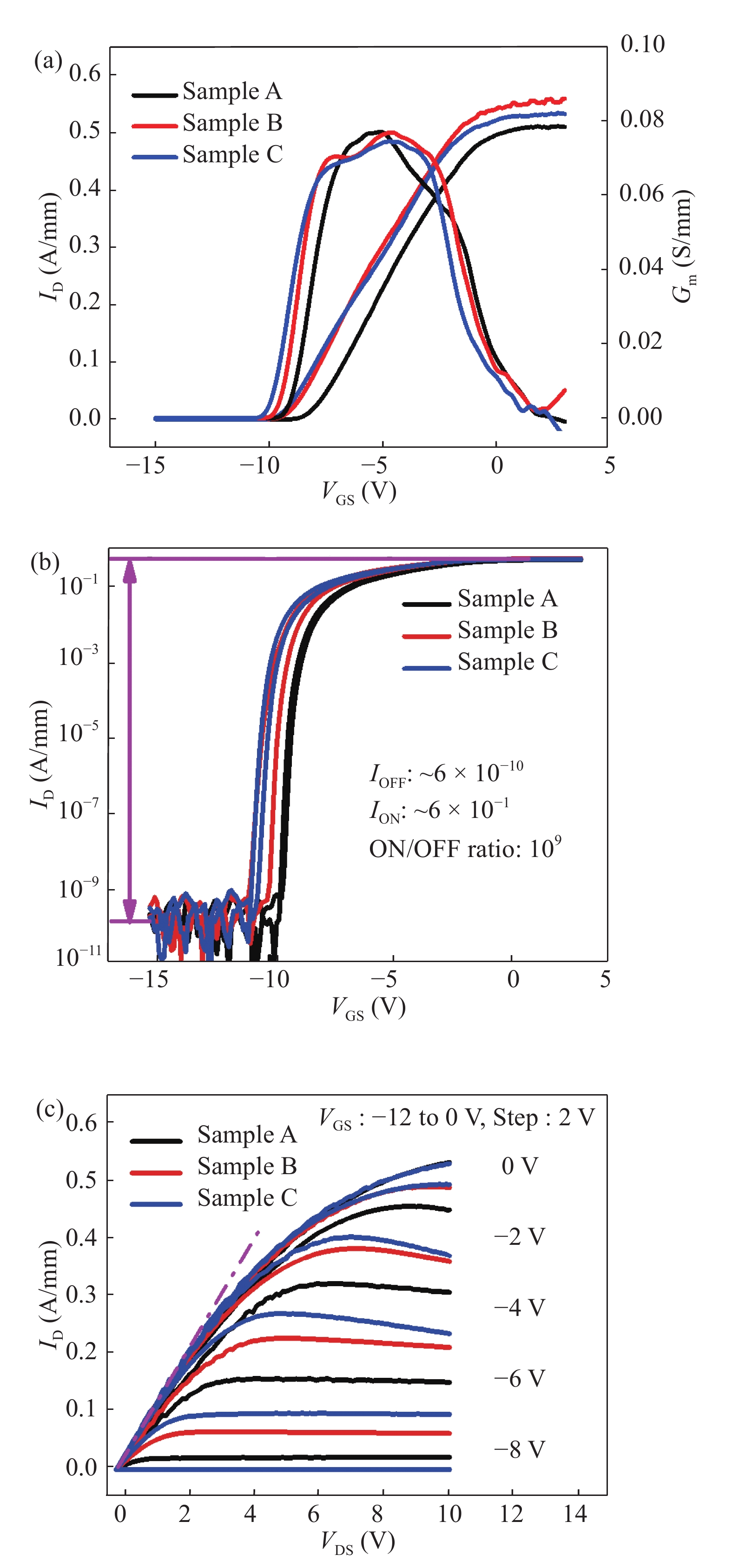
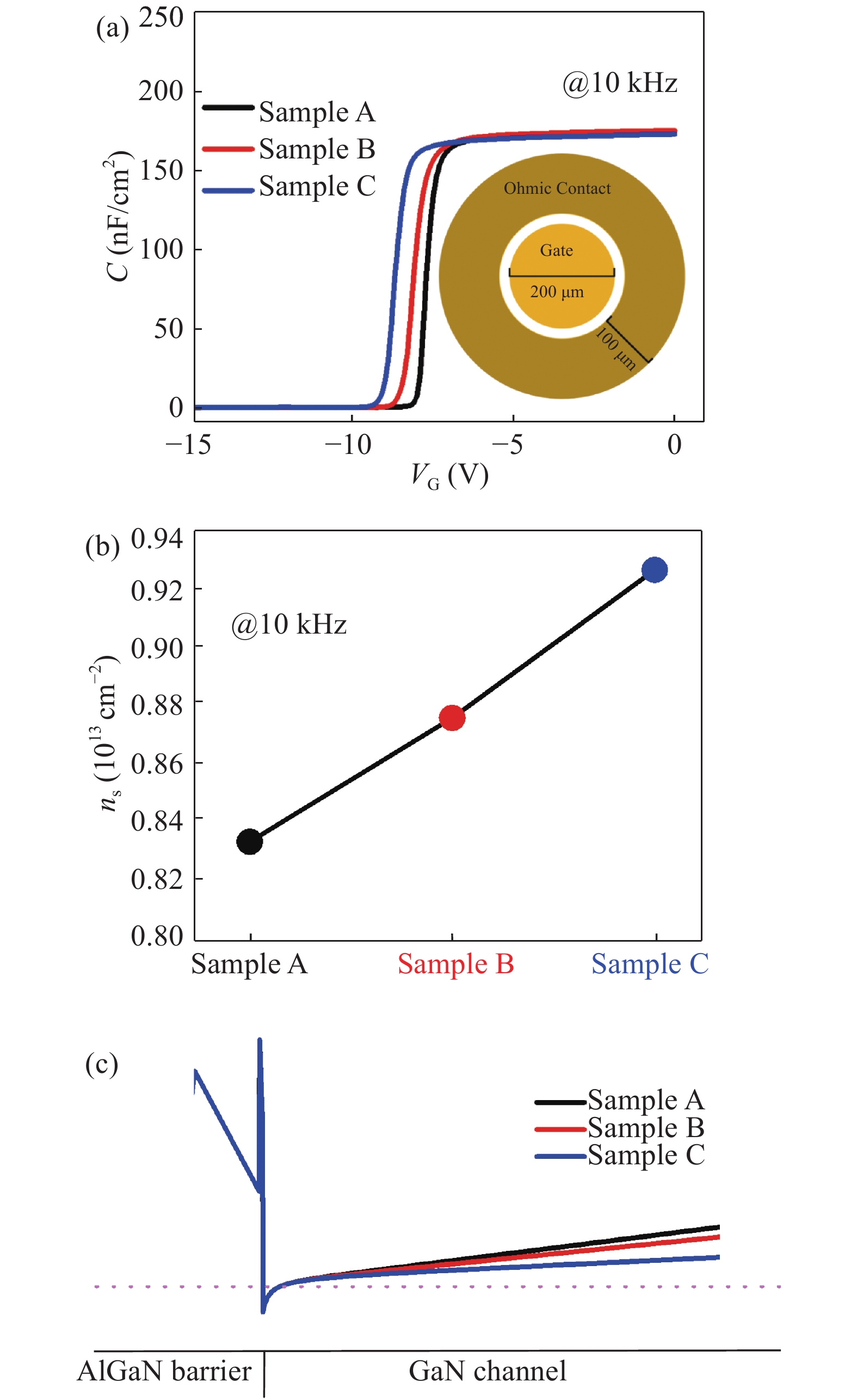
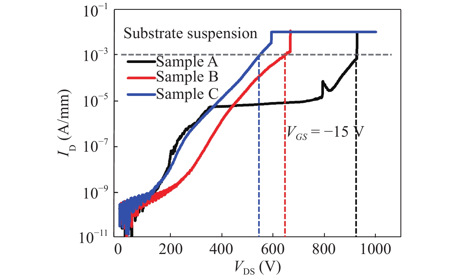
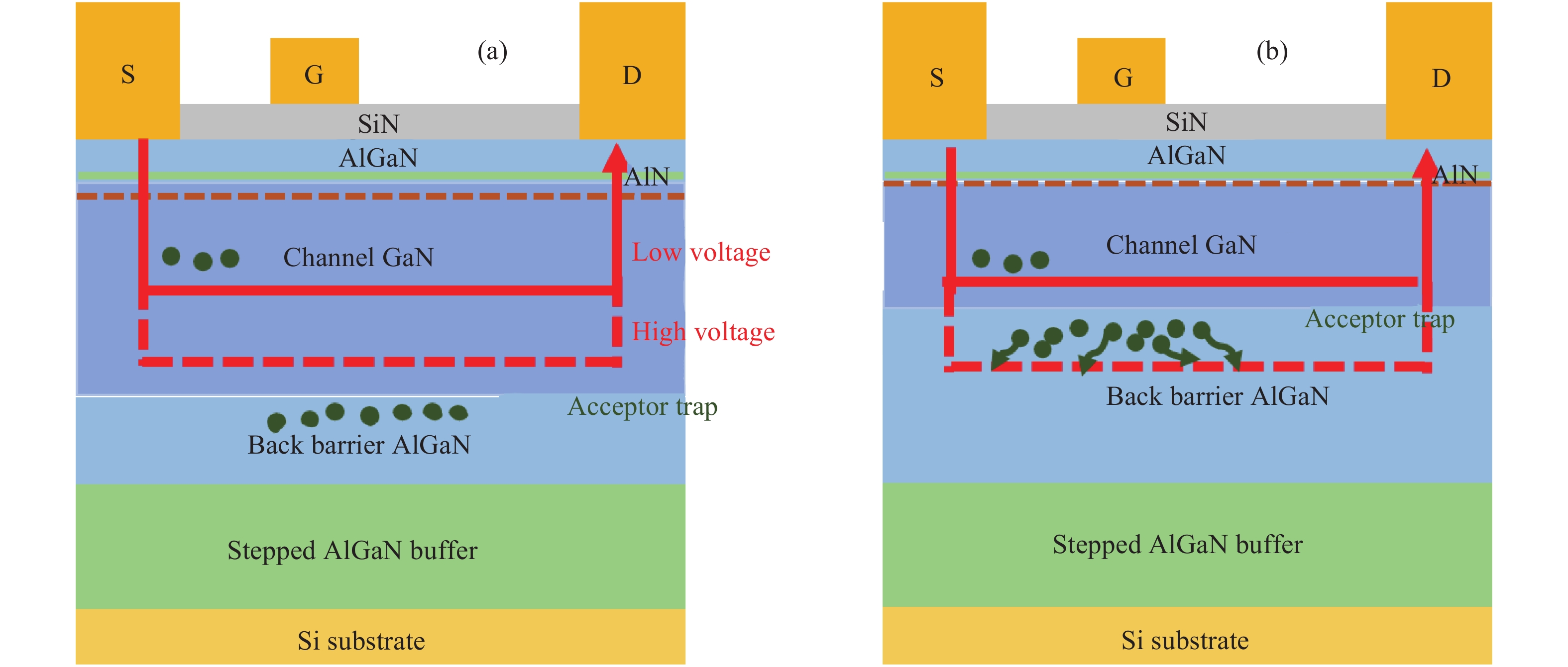
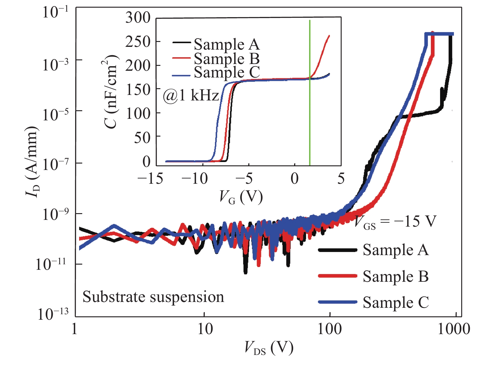
Table 1. Summary of the main DC characterization results.
| Parameter | Ron (Ω·mm) | Saturation current (mA/mm) | Subthreshold swing (mV/dec) | Maximum Gm (mS/mm) |
| Sample A | 11.9 | 530.0 | 75.2 | 77.2 |
| Sample B | 10.7 | 528.5 | 80.3 | 76.9 |
| Sample C | 10.3 | 527.8 | 95.3 | 74.3 |
 DownLoad: CSV
| [1] |
Ueda T, Ishida M, Tanaka T, et al. GaN transistors on Si for switching and high-frequency applications. Jpn J Appl Phys, 2014, 53(10): 100214 doi: 10.7567/JJAP.53.100214
|
| [2] |
Xin T, Yuan J, Gu G, et al. High performance AlGaN/GaN HEMTs with AlN/SiNx passivation. J Semicond, 2015, 36(7): 074008 doi: 10.1088/1674-4926/36/7/074008
|
| [3] |
Yatabe Z, Asubar J T, Hashizume T. Insulated gate and surface passivation structures for GaN-based power transistors. J Phys D, 2016, 49(39): 393001 doi: 10.1088/0022-3727/49/39/393001
|
| [4] |
Zhang Z, Qin S, Fu K, et al. Fabrication of normally-off AlGaN/GaN metal–insulator–semiconductor high-electron-mobility transistors by photo-electrochemical gate recess etching in ionic liquid. Appl Phys Express, 2016, 9(8): 084102 doi: 10.7567/APEX.9.084102
|
| [5] |
Katsuno T, Manaka T, Ishikawa T, et al. Current collapse imaging of Schottky gate AlGaN/GaN high electron mobility transistors by electric field-induced optical second-harmonic generation measurement. Appl Phys Lett, 2014, 104(25): 1742
|
| [6] |
Medjdoub F, Zegaoui M, Grimbert B, et al. Effects of AlGaN back barrier on AlN/GaN-on-silicon high-electron-mobility transistors. Appl Phys Express, 2011, 4(12): 4101
|
| [7] |
Bahat-Treidel E, Hilt O, Brunner F, et al. Punch-through voltage enhancement scaling of AlGaN/GaN HEMTs using AlGaN double heterojunction confinement. IEEE Trans Electron Devices, 2008, 55(12): 3354 doi: 10.1109/TED.2008.2006891
|
| [8] |
Kelekci O, Tasli P, Cetin S S, et al. Investigation of AlInN HEMT structures with different AlGaN buffer layers grown on sapphire substrates by MOCVD. Curr Appl Phys, 2012, 12(6): 1600 doi: 10.1016/j.cap.2012.05.040
|
| [9] |
Ravikiran L, Dharmarasu N, Radhakrishnan K, et al. Growth and characterization of AlGaN/GaN/AlGaN double-heterojunction high-electron-mobility transistors on 100-mm Si(111) using ammonia-molecular beam epitaxy. J Appl Phys, 2015, 117(2): 091003
|
| [10] |
Wang X, Huang S, Zheng Y, et al. Effect of GaN channel layer thickness on DC and RF performance of GaN HEMTs with composite AlGaN/GaN buffer. IEEE Trans Electron Devices, 2014, 61(5): 1341 doi: 10.1109/TED.2014.2312232
|
| [11] |
Zanandrea A, Bahat-Treidel E, Rampazzo F, et al. Single- and double-heterostructure GaN-HEMTs devices for power switching applications. Microelectron Reliab, 2012, 52(9/10): 2426
|
| [12] |
Hsiao Y L, Chang C A, Chang E, et al. Material growth and device characterization of AlGaN/GaN single-heterostructure and AlGaN/GaN/AlGaN double-heterostructure field effect transistors on Si substrates. Appl Phys Express, 2014, 7(5): 055501 doi: 10.7567/APEX.7.055501
|
| [13] |
Wang W J, Li L A, He L, et al. Influence of AlGaN back barrier layer thickness on the dynamic RON characteristics of AlGaN/GaN HEMTs. 2016 13th China International Forum on Solid State Lighting: International Forum on Wide Bandgap Semiconductors China (Sslchina: Ifws), 2016: 77
|
| [14] |
Liu C, Yang S, Liu S H, et al. Thermally stable enhancement-mode GaN metal–isolator–semiconductor high-electron-mobility transistor with partially recessed fluorine-implanted barrier. IEEE Electron Device Lett, 2015, 36(4): 318 doi: 10.1109/LED.2015.2403954
|
| [15] |
Bao Q, Huang S, Wang X, et al. Effect of interface and bulk traps on the C–V characterization of a LPCVD-SiNx/AlGaN/ GaN metal–insulator–semiconductor structure. Semicond Sci Technol, 2016, 31(6): 065014 doi: 10.1088/0268-1242/31/6/065014
|
| [16] |
Marino F A, Bisi D, Meneghini M, et al. Analysis of off-state leakage mechanisms in GaN-based MIS-HEMTs: Experimental data and numerical simulation. Solid-State Electron, 2015, 113: 9 doi: 10.1016/j.sse.2015.05.012
|
| [17] |
Armstrong A, Poblenz C, Green D S, et al. Impact of substrate temperature on the incorporation of carbon-related defects and mechanism for semi-insulating behavior in GaN grown by molecular beam epitaxy. Appl Phys Lett, 2006, 88(8): 8456
|
| [18] |
Zhou C, Jiang Q, Huang S, et al. Vertical leakage/breakdown mechanisms in AlGaN/GaN-on-Si devices. IEEE Electron Device Lett, 2012, 33(8): 1132 doi: 10.1109/LED.2012.2200874
|
| [19] |
Fagerlind M, Allerstam F, Sveinbjörnsson E Ö, et al. Investigation of the interface between silicon nitride passivations and AlGaN/AlN/GaN heterostructures by C–V characterization of metal–insulator–semiconductor heterostructure capacitors. J Appl Phys, 2010, 108(1): 268
|


Article views: 6510 Times PDF downloads: 318 Times Cited by: 0 Times
Received: 09 February 2018 Revised: 23 March 2018 Online: Uncorrected proof: 23 May 2018Accepted Manuscript: 05 July 2018Published: 01 September 2018
| Citation: |
Jie Zhao, Yanhui Xing, Kai Fu, Peipei Zhang, Liang Song, Fu Chen, Taotao Yang, Xuguang Deng, Sen Zhang, Baoshun Zhang. Influence of channel/back-barrier thickness on the breakdown of AlGaN/GaN MIS-HEMTs[J]. Journal of Semiconductors, 2018, 39(9): 094003. doi: 10.1088/1674-4926/39/9/094003
****
J Zhao, Y H Xing, K Fu, P P Zhang, L Song, F Chen, T T Yang, X G Deng, S Zhang, B S Zhang, Influence of channel/back-barrier thickness on the breakdown of AlGaN/GaN MIS-HEMTs[J]. J. Semicond., 2018, 39(9): 094003. doi: 10.1088/1674-4926/39/9/094003.

|
| [1] |
Ueda T, Ishida M, Tanaka T, et al. GaN transistors on Si for switching and high-frequency applications. Jpn J Appl Phys, 2014, 53(10): 100214 doi: 10.7567/JJAP.53.100214
|
| [2] |
Xin T, Yuan J, Gu G, et al. High performance AlGaN/GaN HEMTs with AlN/SiNx passivation. J Semicond, 2015, 36(7): 074008 doi: 10.1088/1674-4926/36/7/074008
|
| [3] |
Yatabe Z, Asubar J T, Hashizume T. Insulated gate and surface passivation structures for GaN-based power transistors. J Phys D, 2016, 49(39): 393001 doi: 10.1088/0022-3727/49/39/393001
|
| [4] |
Zhang Z, Qin S, Fu K, et al. Fabrication of normally-off AlGaN/GaN metal–insulator–semiconductor high-electron-mobility transistors by photo-electrochemical gate recess etching in ionic liquid. Appl Phys Express, 2016, 9(8): 084102 doi: 10.7567/APEX.9.084102
|
| [5] |
Katsuno T, Manaka T, Ishikawa T, et al. Current collapse imaging of Schottky gate AlGaN/GaN high electron mobility transistors by electric field-induced optical second-harmonic generation measurement. Appl Phys Lett, 2014, 104(25): 1742
|
| [6] |
Medjdoub F, Zegaoui M, Grimbert B, et al. Effects of AlGaN back barrier on AlN/GaN-on-silicon high-electron-mobility transistors. Appl Phys Express, 2011, 4(12): 4101
|
| [7] |
Bahat-Treidel E, Hilt O, Brunner F, et al. Punch-through voltage enhancement scaling of AlGaN/GaN HEMTs using AlGaN double heterojunction confinement. IEEE Trans Electron Devices, 2008, 55(12): 3354 doi: 10.1109/TED.2008.2006891
|
| [8] |
Kelekci O, Tasli P, Cetin S S, et al. Investigation of AlInN HEMT structures with different AlGaN buffer layers grown on sapphire substrates by MOCVD. Curr Appl Phys, 2012, 12(6): 1600 doi: 10.1016/j.cap.2012.05.040
|
| [9] |
Ravikiran L, Dharmarasu N, Radhakrishnan K, et al. Growth and characterization of AlGaN/GaN/AlGaN double-heterojunction high-electron-mobility transistors on 100-mm Si(111) using ammonia-molecular beam epitaxy. J Appl Phys, 2015, 117(2): 091003
|
| [10] |
Wang X, Huang S, Zheng Y, et al. Effect of GaN channel layer thickness on DC and RF performance of GaN HEMTs with composite AlGaN/GaN buffer. IEEE Trans Electron Devices, 2014, 61(5): 1341 doi: 10.1109/TED.2014.2312232
|
| [11] |
Zanandrea A, Bahat-Treidel E, Rampazzo F, et al. Single- and double-heterostructure GaN-HEMTs devices for power switching applications. Microelectron Reliab, 2012, 52(9/10): 2426
|
| [12] |
Hsiao Y L, Chang C A, Chang E, et al. Material growth and device characterization of AlGaN/GaN single-heterostructure and AlGaN/GaN/AlGaN double-heterostructure field effect transistors on Si substrates. Appl Phys Express, 2014, 7(5): 055501 doi: 10.7567/APEX.7.055501
|
| [13] |
Wang W J, Li L A, He L, et al. Influence of AlGaN back barrier layer thickness on the dynamic RON characteristics of AlGaN/GaN HEMTs. 2016 13th China International Forum on Solid State Lighting: International Forum on Wide Bandgap Semiconductors China (Sslchina: Ifws), 2016: 77
|
| [14] |
Liu C, Yang S, Liu S H, et al. Thermally stable enhancement-mode GaN metal–isolator–semiconductor high-electron-mobility transistor with partially recessed fluorine-implanted barrier. IEEE Electron Device Lett, 2015, 36(4): 318 doi: 10.1109/LED.2015.2403954
|
| [15] |
Bao Q, Huang S, Wang X, et al. Effect of interface and bulk traps on the C–V characterization of a LPCVD-SiNx/AlGaN/ GaN metal–insulator–semiconductor structure. Semicond Sci Technol, 2016, 31(6): 065014 doi: 10.1088/0268-1242/31/6/065014
|
| [16] |
Marino F A, Bisi D, Meneghini M, et al. Analysis of off-state leakage mechanisms in GaN-based MIS-HEMTs: Experimental data and numerical simulation. Solid-State Electron, 2015, 113: 9 doi: 10.1016/j.sse.2015.05.012
|
| [17] |
Armstrong A, Poblenz C, Green D S, et al. Impact of substrate temperature on the incorporation of carbon-related defects and mechanism for semi-insulating behavior in GaN grown by molecular beam epitaxy. Appl Phys Lett, 2006, 88(8): 8456
|
| [18] |
Zhou C, Jiang Q, Huang S, et al. Vertical leakage/breakdown mechanisms in AlGaN/GaN-on-Si devices. IEEE Electron Device Lett, 2012, 33(8): 1132 doi: 10.1109/LED.2012.2200874
|
| [19] |
Fagerlind M, Allerstam F, Sveinbjörnsson E Ö, et al. Investigation of the interface between silicon nitride passivations and AlGaN/AlN/GaN heterostructures by C–V characterization of metal–insulator–semiconductor heterostructure capacitors. J Appl Phys, 2010, 108(1): 268
|

 WeChat ID
Journal of Semiconductors © 2017 All Rights Reserved 京ICP备05085259号-2


