| [1] |
Geller S. Crystal Structure of β‐Ga2O3. J Chem Phys, 1960, 33: 676 doi: 10.1063/1.1731237 |
| [2] |
Roy R, Hill V G, and Osborn E F J. Polymorphism of Ga2O3 and the System Ga2O3—H2O. Am Chem Soc, 1952, 74:719 doi: 10.1021/ja01123a039 |
| [3] |
Tippins H H. Optical Absorption and Photoconductivity in the Band Edge of β−Ga2O3. Phys Rev, 1965, 140:A316 doi: 10.1103/PhysRev.140.A316 |
| [4] |
Hajnal Z, Miro J, Kiss G, Reti F, Deak P, Herndon R C, and Kuperberg J M. Role of oxygen vacancy defect states in the n-type conduction of β-Ga2O3. J Appl Phys, 1999, 86:3792 doi: 10.1063/1.371289 |
| [5] |
Kohn J A, Katz G and Broder J D. Characterization of β-Ga2O3 and its Alumina Isomorph θ-Al2O3. Am Mineral, 1956, 42:398
|
| [6] |
Wolten G M and Chase A B. Determination of the point group of β-Ga2O3 from morphology and physical properties. J Solid State Chem, 1976, 16: 377 doi: 10.1016/0022-4596(76)90054-2 |
| [7] |
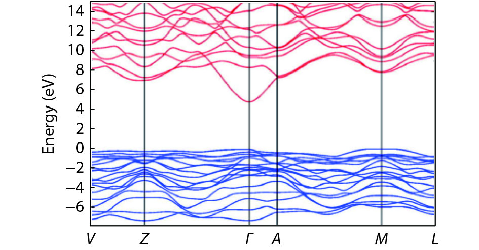
Ahman J, Svensson G and Albertsson J. A reinvestigation of β-gallium oxide. Acta Crystallogr Sect C Cryst Struct Commun,1996, 52: 1336 doi: 10.1107/S0108270195016404 |
| [8] |
Janowitz C, Scherer V, Mohamed M, Krapf A, Dwelk H, Manzke R, Galazka Z, Uecker R, Irmscher K and Fornari R. Experimental electronic structure of In 2O 3 and Ga 2O 3. New J Phys, 2011, 13:085014. doi: 10.1088/1367-2630/13/8/085014 |
| [9] |
Yoshioka S, Hayashi H, Kuwabara A, Oba F, Matsunaga K and Tanaka I. Structures and energetics of Ga2O3 polymorphs. J Phys Condens Matter, 2007, 19: 346211 doi: 10.1088/0953-8984/19/34/346211 |
| [10] |
Yamaguchi K. First principles study on electronic structure of β-Ga2O3. Solid State Commun, 2004,131:739 doi: 10.1016/j.ssc.2004.07.030 |
| [11] |
He H, Orlando R, Blanco M, Pandey R, and Rétat M. First-principles study of the structural, electronic, and optical properties of Ga2O3 in its monoclinic and hexagonal phases. Phys Rev B, 2006, 74:195123 doi: 10.1103/PhysRevB.74.195123 |
| [12] |
Zhang Y, Yan J, Zhao G and Xie W. First-principles study on electronic structure and optical properties of Sn-doped β-Ga2O3. Phys B Condens Matter, 2010, 405:3899 doi: 10.1016/j.physb.2010.06.024 |
| [13] |
Zhang L, Yan J, Zhang Y, Li T and Ding X. First principles study on electronic structure and optical properties of N-doped P-type β-Ga2O3. Sci China Physics, Mech Astron, 2012, 55:19 doi: 10.1007/s11433-011-4582-8 |
| [14] |
Peelaers H and Van de Walle C G. Brillouin zone and band structure of β‐Ga2O3. Phys Status Solidi (B), 2015, 252:828 doi: 10.1002/pssb.201451551 |
| [15] |
Varley J B, Weber J R, Janotti A and Van de Walle C G. Oxygen vacancies and donor impurities in β‐Ga2O3. Appl Phys Lett, 2010, 97:142106 doi: 10.1063/1.3499306 |
| [16] |
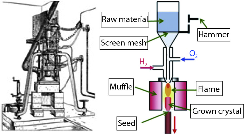
Nassau K. Dr. A. V. L. Verneuil: The man and the method. J of Cry Growth, 1972, 13:12
|
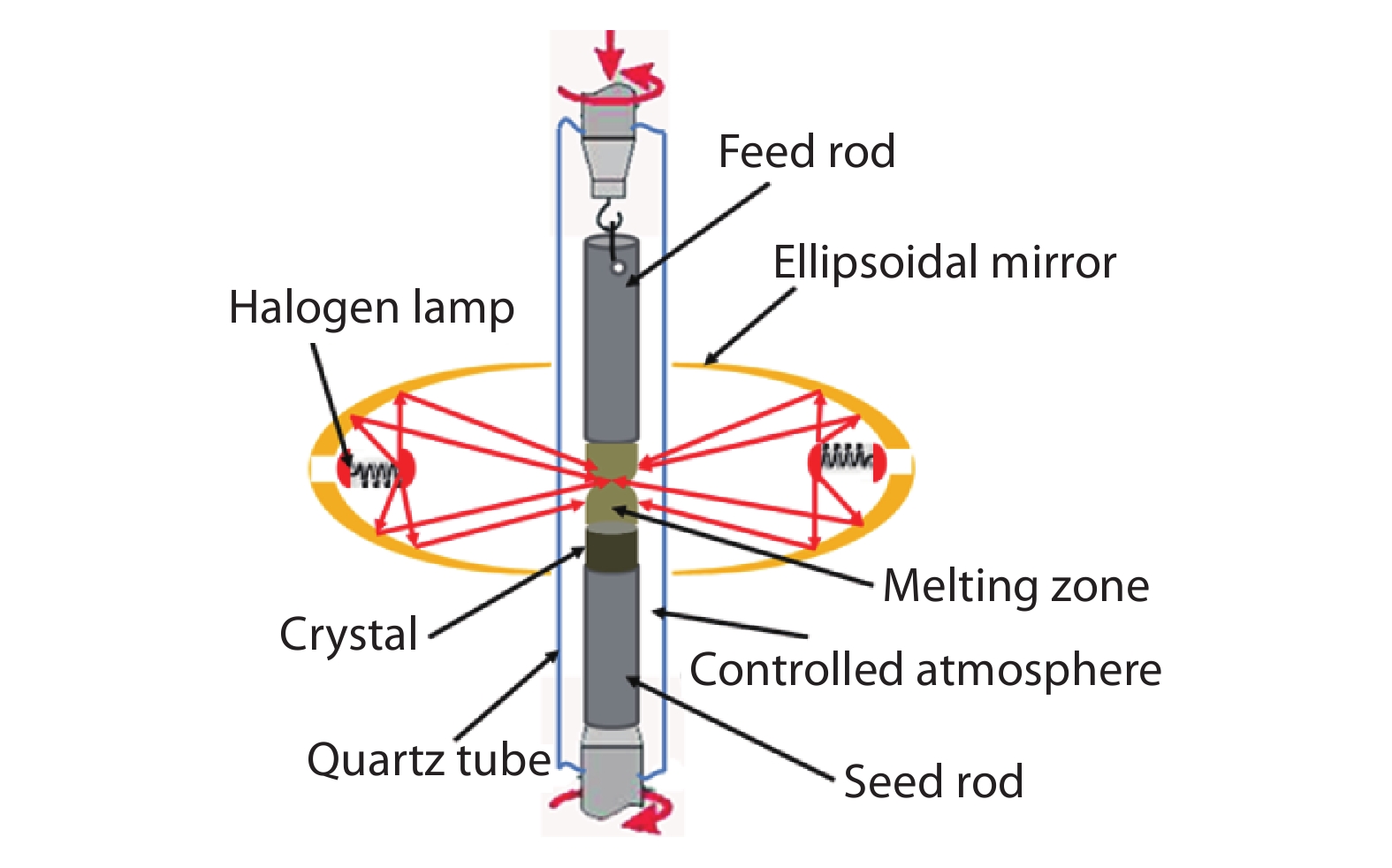
| [17] |
Chase A B. Growth of β‐Ga2O3 by the Verneuil Technique. J Am Ceram Soc, 1964, 47: 470
|
| [18] |
Lorenz M R, Woods J F, Gambino R J. Some electrical properties of the semiconductor βGa2O3. J Phys Chem Solids, 1967, 28:403 doi: 10.1016/0022-3697(67)90305-8 |
| [19] |
Harwig T and Schoonman J. Electrical properties of β-Ga2O3 single crystals. II. Journal of Solid State Chemistry, 1978, 23: 205 doi: 10.1016/0022-4596(78)90066-X |
| [20] |
Harwig T, Wubs G J, and Dirksen G J. Electrical properties of β-Ga2O3 single crystals. Solid State Communications, 1976, 18:1223 doi: 10.1016/0038-1098(76)90944-3 |
| [21] |
Theurer H C. Method of processing semiconductive materials. U. S. Patent 3,060,123 (Filed December 17, 1952. Issued October 23, 1962)
|
| [22] |
Víllora E G, Shimamura K, Yoshikawa Y, Aoki K, and Ichinose N. Large-size β-Ga2O3 single crystals and wafers. Journal of Crystal Growth, 2004, 270:420. doi: 10.1016/j.jcrysgro.2004.06.027 |
| [23] |
Zhang J, Li B, Xia C, Pei G, Deng Q, Yang Z, Wusheng X, Hongsheng Shi, Feng W, Yongqing W, Jun X. Growth and spectral characterization of β-Ga2O3 single crystals. Journal of Physics and Chemistry of Solids, 2006, 67: 2448 doi: 10.1016/j.jpcs.2006.06.025 |
| [24] |
Czochralski J. A new method for the measurement of the crystallization rate of metals. Zeitschrift für Physikalische Chemie, 1918, 92: 219
|
| [25] |
Galazka Z, Uecker R, Irmscher K, Albrecht M, Klimm D, Pietsch M. Czochralski growth and characterization of β‐Ga2O3 single crystals. Crystal Research and Technology, 2010, 45: 1229 doi: 10.1002/crat.v45.12 |
| [26] |
Tomm Y, Reiche P, Klimm D, and Fukuda T. Czochralski grown Ga2O3 crystals. Journal of Crystal Growth, 2000, 220: 510 doi: 10.1016/S0022-0248(00)00851-4 |
| [27] |
Galazka Z, Uecker R, Klimm D, Irmscher K, Naumann M, Pietsch M, Kwasniewski A, Bertram R, Ganschow S and Bickermann M. Scaling-Up of Bulk β-Ga2O3 Single Crystals by the Czochralski Method. ECS Journal of Solid State Science and Technology, 2017,6: Q3007 doi: 10.1149/2.0021702jss |
| [28] |
Galazka Z, Ganschow S, Fiedler A, Bertam R, Klimm D, Irmscher K, Schewski R, Pietsch M, Albercht M, and Bichermann M. Doping of Czochralski-grown bulk β-Ga2O3 single crystals with Cr, Ce and Al. J Cry Growth, 2018, 486:82 doi: 10.1016/j.jcrysgro.2018.01.022 |
| [29] |
Chalmers B, LaBelle Jr H E, and Mlavsky A I. Growth of controlled profile crystals from the melt: Part III — Theory. Materials Research Bulletin, 1971, 6: 681 doi: 10.1016/0025-5408(71)90101-2 |
| [30] |
LaBelle Jr H E and Mlavsky A. Growth of controlled profile crystals from the melt: Part I - Sapphire filaments. Materials Research Bulletin, 1971, 6: 571 doi: 10.1016/0025-5408(71)90006-7 |
| [31] |
LaBelle Jr H. Growth of controlled profile crystals from the melt: Part II - Edge-defined, film-fed growth (EFG). Materials Research Bulletin, 1971, 6: 581 doi: 10.1016/0025-5408(71)90007-9 |
| [32] |
Aida H, Nishiguchi K, Takeda H, Aota N, Sunakawa K, and Yaguchi Y. Growth of β-Ga2O3 single crystals by the edge-defined, film fed growth method. Japanese Journal of Applied Physics, 2008,47: 8506 doi: 10.1143/JJAP.47.8506 |
| [33] |
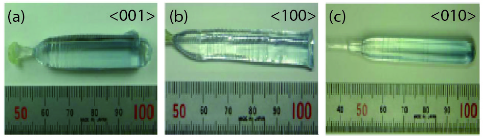
Mu We, Jia Zh, Yin Y, Hu Qg , Li Y, Wu B, Zhang J, Tao X. High quality crystal growth and anisotropic physical characterization of β-Ga2O3 single crystals grown by EFG method. Journal of Alloys and Compounds, 2017, 714, 453:458
|
| [34] |
Kuramata A, Koshi K, Watanabe Sh, Yamaoka Yu, Masui T and Yamakoshi Sh. High-quality β-Ga2O3 single crystals grown by edge-defined film-fed growth. Japanese Journal of Applied Physics, 2016, 55: 1202A2
|
| [35] |
Kuramata A, Koshi K, Watanabe Sh, et al. Bulk crystal growth of Ga2O3. Proc SPIE 10533, Oxide-based Materials and Devices IX, 2018, 105330E
|
| [36] |
Zhang Sh, Lian X, Ma Y, Liu W , Zhang Y , Xu Y and Cheng H. Growth and characterization of 2-inch high quality β-Ga2O3 single crystals grown by EFG method. Journal of Semiconductors. 2018, 39: 083003 doi: 10.1088/1674-4926/39/8/083003 |
| [37] |
Bridgman Percy W. Certain physical properties of single crystals of tungsten, antimony, bismuth, tellurium, cadmium, zinc, and tin. Proceedings of the American Academy of Arts and Sciences. 1925, 60 : 305 doi: 10.2307/25130058 |
| [38] |
Stockbarger D C. The production of large single crystals of lithium fluoride. Review of Scientific Instruments, 1936 7: 133 doi: 10.1063/1.1752094 |
| [39] |
Hoshikawa K, Ohba E, Kobayashi T, Yanagisawa J, Miyagawa C, and Nakamura Y. Growth of β-Ga2O3 single crystals using vertical Bridgman method in ambient air. Journal of Crystal Growth, 2016, 447: 36 doi: 10.1016/j.jcrysgro.2016.04.022 |
| [40] |
Ohba E, Kobayashi T, Kado M, and Hoshikawa K. Defect characterization of β-Ga2O3 single crystals grown by vertical Bridgman method. Japanese Journal of Applied Physics, 2016, 55:1202BF doi: 10.7567/JJAP.55.1202BF |
| [41] |
Tsao J Y, Chowdhury S, Hollis M A, Jena D, Johnson N M, Jones K A, Kaplar R J, Rajan S, Van de Walle C G, Bellotti E, Chua C L, Collazo R, Coltrin M E, Cooper J A, Evans K R, Graham S, Grotjohn T A, Heller E R, Higashiwaki M, Islam M S, Juodawlkis P W, Khan M A, Koehler A D, Leach J H, Mishra U K, Nemanich R J, Pilawa-Podgurski R C N, Shealy J B, Tadjer M J, Witulski A F, Wraback M, and Simmons J A.Ultrawide‐Bandgap Semiconductors: Research Opportunities and Challenges. Adv. Electron Mater, 2018, 4:1600501
|
| [42] |
Suzuki N, Ohira S, Tanaka M, Sugawara T, Nakajima K and Shishido T. Fabrication and characterization of transparent conductive Sn‐doped β‐Ga2O3 single crystal. Phys Status Solidi (C), 2007, 4: 2310 doi: 10.1002/(ISSN)1610-1642 |
| [43] |
Ueda N, Hosono H, Waseda R and Kawazoe H. Synthesis and control of conductivity of ultraviolet transmitting single crystals. Appl Phys Lett 1997, 70: 3561 doi: 10.1063/1.119233 |
| [44] |
Ohira S, Suzuki N, Arai N, Tanaka M, Sugawara T, Nakajima K and Shishido T. Characterization of transparent and conducting Sn-doped β-Ga2O3 single crystal after annealing. Thin Solid Films 2008, 516: 5763 doi: 10.1016/j.tsf.2007.10.083 |
| [45] |
VÍllora E G, Shimamura K, Yoshikaw Y, Ujiie T and Aoki K. Electrical conductivity and carrier concentration control in by Si doping. Appl Phys Lett,2008, 92:202120 doi: 10.1063/1.2919728 |
| [46] |
Sasaki K, Higashiwaki M, Kuramata A, Masui T and Yamakoshi S. Si-Ion Implantation Doping in β-Ga2O3 and Its Application to Fabrication of Low-Resistance Ohmic Contacts. Appl Phys Express, 2013, 6 : 6502
|
| [47] |
Zhou W, Xia ch, Sai Q, and Zhang H. Controlling n-type conductivity of β-Ga2O3 by Nb doping. Appl Phys Lett, 2017, 111:242103 doi: 10.1063/1.4994263 |
| [48] |
Mastro M A, Kuramata A, Calkins J, Kim J, Ren F and Pearton S J ECS. Perspective—Opportunities and Future Directions for Ga2O3. J Solid State Sci Technol, 2017,6: P356 doi: 10.1149/2.0031707jss |
| [49] |
Varley J B, Janotti A, Franchini C, and Van de Walle C G. Role of self-trapping in luminescence and-type conductivity of wide-band-gap oxides. Phys Rev B, 2012, 85 :081109 doi: 10.1103/PhysRevB.85.081109 |
| [50] |
Kananen B E, Halliburton L E, Stevens K T, Foundos G K, and Giles N.C. Gallium vacancies in β-Ga2O3 crystals. Appl Phys Lett, 2017, 110: 202104 doi: 10.1063/1.4983814 |
| [51] |
Onuma T, Fujioka S, Yamaguchi T, Higashiwaki M, Sasaki K, Masui T and Honda T. Correlation between blue luminescence intensity and resistivity in β-Ga2O3 single crystals. Appl Phys Lett, 2013, 103 : 2013
|
| [52] |
Liu L L, Li M K, Yu D Q, Zhang J, Zhang H, Qian C and Yang Z. Fabrication and characteristics of N-doped β-Ga2O3 nanowires. Appl Phys A, 2010, 98: 831
|
| [53] |
Dong L, Jia R, Li C, Xin B, and Zhang Y. Ab initio study of N-doped β-Ga2O3 with intrinsic defects: the structural, electronic and optical properties. J Alloys Compd, 2017, 712:379 doi: 10.1016/j.jallcom.2017.04.020 |
| [54] |
Kyrtsos A, Matsubara M, and Bellotti E. On the feasibility of p-type Ga2O3. Appl Phy Lett, 2018, 112:032108 doi: 10.1063/1.5009423 |
| [55] |
Bartic M, Toyoda Y, Baban C-I, and Ogita M. Oxygen sensitivity in gallium oxide thin films and single crystals at high temperatures. Jpn. J Appl Phys, 2006, 45: 5186 doi: 10.1143/JJAP.45.5186 |
| [56] |
Hudgins J L, Simin G S, Santi E and Khan M A. An assessment of wide bandgap semiconductors for power devices. IEEE Trans. Power Electron. 2003,18: 907. doi: 10.1109/TPEL.2003.810840 |
| [57] |
Higashiwaki M, Sasaki K, Murakami H, Kumagai Y, Koukitu A, Kuramata A, Masui T, and Yamakoshi S. Recent progress in Ga2O3 power devices. Semiconductor Science and Technology, 2016, 31: 034001 doi: 10.1088/0268-1242/31/3/034001 |
| [58] |
Higashiwaki M, Sasaki K, Kuramata A, Masui T, and Yamakoshi S. Development of gallium oxide power devices, Physica Status Solidi (a) ,2014, 211: 21 doi: 10.1002/pssa.201330197 |
| [59] |
Oishi T, Koga Y, Harada K and Kasu M. High-mobility β-Ga2O3(201) single crystals grown by edge-defined film-fed growth method and their Schottky barrier diodes with Ni contact. Appl Phys Express, 2015, 8 : 031101 doi: 10.7567/APEX.8.031101 |
| [60] |
Sasaki K, Higashiwaki M, Kuramata A, Masui T, and Yamakoshi S. Ga2O3 Schottky Barrier Diodes Fabricated by Using Single-Crystal β-Ga2O3(010) Substrates. IEEE Electron Device Letters, 2013, 34: 493 doi: 10.1109/LED.2013.2244057 |
| [61] |
Hu Z Z, Zhou H, Feng Q, Zhang J C, Zhang C F, Dang K, Cai Y C, Feng Z Q, Gao Y Y, Hao Y. Field-Plated Lateral β-Ga2O3 Schottky Barrier Diode With High Reverse Blocking Voltage of More Than 3 kV and High DC Power Figure-of-Merit of 500 MW/cm2. IEEE Electron Device Letters, 2018, 39:1564-7
|
| [62] |
Higashiwaki M, Sasaki K, Kuramata A, Masui T, and Yamakoshi S. Gallium oxide (Ga2O3) metal-semiconductor field-effect transistors on single-crystal β-Ga2O3 (010) substrates. Applied Physics Letters, 2012, 100: 013504 doi: 10.1063/1.3674287 |
| [63] |
A. J. Green, K. D. Chabak, E. R. Heller, R. C. Fitch, M. Baldini, A. Fiedler, K. Irmscher, G. Wagner, Z. Galazka, S. E. Tetlak, Crespo A, Leedy K, and Jessen G H. 3.8-MV/cm Breakdown Strength of MOVPE-Grown Sn-Doped β-Ga2O3 MOSFETs. IEEE Electron Device Letters, 2016, 37: 902 doi: 10.1109/LED.2016.2568139 |
| [64] |
Suzuki R, Nakagomi S, Kokubun Y, Arai N and Ohira S. Enhancement of responsivity in solar-blind photodiodes with a Au Schottky contact fabricated on single crystal substrates by annealing. Appl Phys Lett, 2009, 94: 222102 doi: 10.1063/1.3147197 |
| [65] |
Yang C, Liang H, Zhang Z, Xia X, Tao P, Chen Y, Zhang H, Shen R, Luo Y and Du G. Self-powered SBD solar-blind photodetector fabricated on the single crystal of β-Ga2O3. RSC Adv, 2018, 8:6341 doi: 10.1039/C8RA00523K |
| [66] |
Patrick E, Choudhury M, Ren F, Pearton S J, and Law M. Simulation of Radiation Effects in AlGaN/GaN HEMTs ECS J Solid State Sci Technol, 2015, 4, Q21 doi: 10.1149/2.0181503jss |
| [67] |
Yang J, Ren F, Pearton S J, Yang G, Kim J, and Kuramata A.1.5 MeV electron irradiation damage in β-Ga2O3 vertical rectifiers, J Vac Sci Technol B, 2017, 35, 031208 doi: 10.1116/1.4983377 |
| [68] |
Szalkai D, Galazka Z, Irmscher K, Tütt˝o P, Klix A and Gehre D. β-Ga2O3 Solid-State Devices for Fast Neutron Detection. IEEE Transactions on Nuclear Science, 2017, 64, 6: 1248 doi: 10.1109/TNS.2017.2656298 |


 DownLoad: